Carbon nanotubes are clean 1D systems that have been shown to behave like a Luttinger liquid at high electron density. 27 4 The one-dimensional Wigner crystal in carbon nanotubes 31 5 Observation of a Mott insulating state in carbon nanotubes 48 6 Simultaneous electrical and Raman spectroscopy measurements 59. 1D systems such as carbon nanotubes [3], molecular beam epitaxy (MBE) growth cleaved-edge quantum wires [4] and edge conditions of the fractional quantum Hall effect (FQHE) in 2DEGs [5] were used to verify that the 1D electron gas is indeed a Luttinger liquid.
Carbon nanotubes; electronic and thermal properties
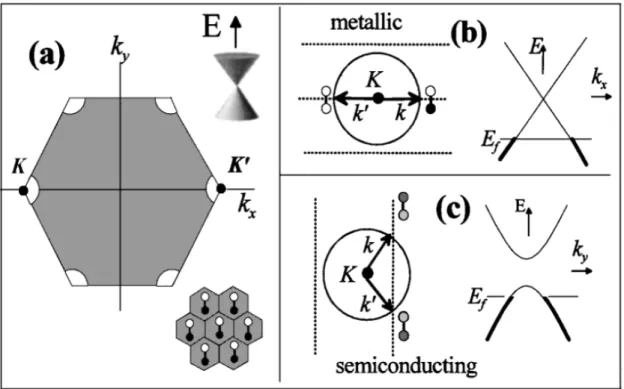
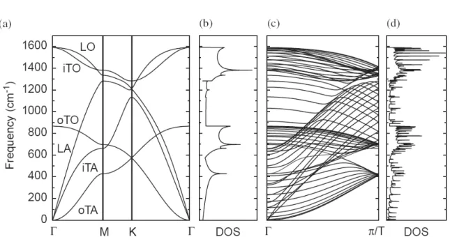
For example, this results in translation of the Dirac points of graphene and opens a small band gap for most metallic nanotubes. For the purposes of this thesis, nanotubes with .kBT energy gaps at room temperature will be referred to as "metallic", "quasi-metallic", or "small band gap". Similar to the band structure, the quantized phonon dispersion of nanotubes can be obtained by area folding the phonon dispersion of graphite [14].
Overview of concepts and techniques
Another effect important in small systems is the discretization of the energy spectrum due to the formation of zero-dimensional (0D) electron states. Raman spectroscopy involves the inelastic scattering of monochromatic light, usually from a laser in the visible, near-infrared, or near-ultraviolet range, by phonons and other low-frequency excitations of the system. The elastically scattered light is filtered out and the rest of the light is collected on a detector.
Previous work
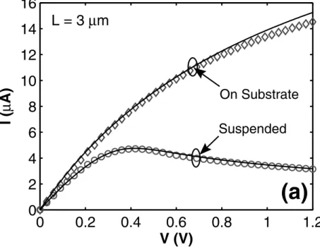
Alternative models for the T dependence of thermal conductivity (eg, constant T, or T decreasing linearly in T) cannot be reproduced. Depending on the size of the channel, electron beam or optical beam lithography is used to pattern the channel. At high bias (typically up to 1.5–2 V), all nanotube shells carry current, approximately in equal amounts.
Luttinger liquid formalism
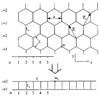
These processes are dominated by the short-term part of the interaction, at distances r ~ a, where the interaction changes significantly from place to place. The Hamiltonian can be written for the charge sector only as Hρ = H0(θρ+, φρ+) +Hint(θρ+) and can be written as 3.4) This describes a 1D acoustic plasmon propagating with velocity. Neglecting backscattering processes, i.e. short-range limit at a diameter of 2r, which is larger than the atomic spacing.
Inclusion of band-curvature: The 1D Wigner crystal
The difference in velocities between the charge and neutral (taste) sectors leads to a separation of energy scales where the charge distance (measured energy gap) ∆ is stiffer than the taste gap by a factor of K1/2; the taste gap, ≈ ∆0, is relatively unaffected by interactions. The charge soliton is limited in space to an area (width wρ) related to ∆ by wρ ∼ ~vρ/∆, where vρ=K1/2vF is the charge mode velocity. As a result of the competition, the electron is localized within a finite region of space, i.e. the soliton width.
Inclusion of umklapp scattering: The Mott insulating state
The size of the resulting Mott gap is given by the energy of the charge soliton. Based on this order-of-magnitude estimate (see, e.g., ref. 9), the Coulomb energy becomes dominant and the system should begin to transition into the strongly interacting regime at n∼aB−1 =me2/~2. Surprisingly, we observe a sudden damping of the Kondo effect for unpaired hole states when the magnetic field is tuned by the transition from the antiferromagnetically ordered regime to the quadruple charge regime.
When B > 0, the Wigner crystal state is a competition between magnetic and exchange energy. The Kondo effect and flavor configurations. a) Color scale plot of Gversus Vg and B. The boundary between regions II and III is indicated by the dashed black line. Up isospin is shown by blue levels, while down isospin is shown by red levels. e) Wigner crystal table of the transition between region II and III.
From the measured parameters of our dot, we estimate the kBTK to be ~0.1 meV at the center of the Coulomb valleys [26], so we expect the total spin and isospin to be significant. An unexpected feature of the Kondo effect is the decrease of Gby ∆G~1.5 µS in the valley of the odd hole when B is aligned from region II to region III. In contrast, the slope of the evolution of the Coulomb peaks depends only on the coupling of the energy of each hole with the magnetic field.
Therefore, determining the quantum number of the added carriers from the Coulomb peak evolution, as we did in the main text, is simpler than using the addition energies.
Supplementary Figure 3
Direct observation of mode selective electron-phonon cou- pling in suspended carbon nanotubes
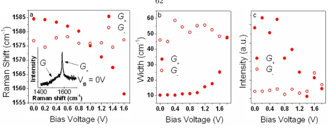
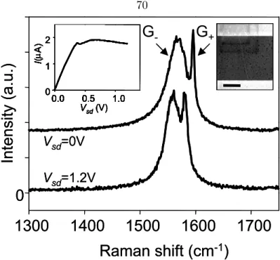
The LO and TO modes of the G band behave differently with respect to voltage bias, indicating preferential electron-phonon coupling and non-equilibrium phonon populations, causing negative differential conductance in pendant devices. In metal nanotubes, the low-frequency component of the G-band (G−) shows a broad Breit-Wigner-Fano (BWF) line shape, and is significantly down-shifted in frequency from its counterpart in semiconducting nanotubes [15]. Recent experiments have shown that this softening of phonons can be removed by shifting the Fermi energy of m-CNTs with an applied gate voltage or chemical doping, which modulates this coupling and results in an upshift of the G-band frequency. ].
This is thought to be caused by the strong attenuation of the LO mode due to the Kohn anomaly, also referred to as a Peierls-like distortion phenomenon [103]. We observe preferential downshifts of only one of the OPs at high currents, indicating strong electron coupling in only one band and a non-equilibrium phonon population. Suspended SWNTs were grown using CVD on Pt electrodes prepared with lithographically patterned catalyst islands.
Of the 40 devices per chip, typically only a few have only one SWNT connecting the device pins. First, a gap is made between two Pt electrodes on a degenerately doped Si substrate by one of two methods34, 35. In the first method, Pt electrodes are patterned by lithography on a Si substrate covered with 300 nm SiO2, e which is then wet etched in HF using Pt electrodes as an etch mask.
Islands of Fe-Mo catalyst salts in an alumina matrix are then defined on top of the contacts in lithographically defined areas36.
4Figure 6.1. SEM image of a suspended carbon nanotube grown on top of Pt electrodes
The line widths of the G + and G bands in the nanotube in Figure 2 also vary with the applied bias voltage. Finally, the intensity of the G+ band decreases monotonically with bias, while the G band remains constant. Preferential heating of the G + phonon was observed in 4 out of 15 devices measured in this study, including one semiconductor device.
Here the voltage dependence of the G+ and G− bands is reversed from that shown in Figure 6.2. Furthermore, the linewidth of the G− band increases significantly with bias and decreases in intensity, while the G+ band remains of constant width and intensity. In contrast to Figure 6.2, these data show preferential heating of the G− band, which we again assign to the LO Γ-point phonon mode.
The NDC can be clearly seen above 1.2 V in the current-voltage (I-Vbias) characteristics of this device, as shown in the inset of Figure 3. Here, the voltage dependence of the G+ and G- bands is reversed from that shown in Figure 2. V in contrast to Fig. 2, these data show a preferential heating of the G band, again attributed to the phonon mode of the LO G-dot. This, together with the lack of change in the TO Stokes Raman frequency, indicates that the TO phonon population remains close to room temperature.
The failure of the model without OP absorption indicates the important role played by the non-equilibrium optical phonon population in the electron transport of suspended SWNTs.
12Figure 6.6. Summary of electron and phonon parameters of 5 suspended nanotubes
Spatially-resolved temperature measurements of electrically- heated carbon nanotubes
We understand these results in terms of decay and thermalization of non-equilibrium phonons. In this case, some phonon modes may have an effective temperature higher than the rest of the lattice, depending on their coupling to the electric current. The G band temperature is obtained at each point along the nanotube by dividing the voltage-induced change in the Raman shift by the slope of the calibration line.
Therefore, the observation that one of the modes in short nanotube devices is not modulated by bias or spacing indicates that the lattice remains at room temperature. 6.10(a) (below) shows, most of the grating is heated because the devices are long enough for the hot phonons to thermalize. Using suitable values for the scattering lengths (as obtained from experiment [34, 35]), λac, RT=1.6µm and λop,min~180 nm, we can obtain a spatial variation of the thermal conductivity.
Thus, the thermal contact resistance provides a significant temperature drop at the ends of the nanotube. This measurement provides insight into the mechanism of thermal transport and provides a measure of the thermal conductivity and thermal contact resistances of carbon nanotubes. From our data, we obtain a measurement of the thermal conductance quantum that is in good agreement.
Our data provide an experimental measurement of the thermal conductivity quantum, which agrees with theoretical predictions as well as with thermal transport results in cryogenically cooled Si3N4. A schematic of the device with the nanotubes on top of the plugs is shown in the inset of Fig. In the locked ON state, subsequent SEM images of the devices show that the gap disappears, indicating the nanomechanical movement of the nanotube shells to physically reunite with the two seg- nanotubes.
8.4, if the device is imaged in the SEM at the intermediate stage or even just exposed to the ambient atmosphere, indicating that the cleanliness of the tube tips is important for stable adhesion. This and the large magnitude of gate-induced bending stress suggest that the nanotube adhesion results from the formation of one or more covalent bonds between the atoms in the tube ends. However, further experiments are needed to fully elucidate the adhesion mechanism, for example high-temperature vacuum annealing of the device post-disassembly, to close and cover the ends of the inner nanotube shells [171].
It is expected that the tube ends will then attach to the smaller van der Waals bonds, enabling the realization of microwave frequency oscillators or charge shuttles, for example. We also note that the observed switching voltage can likely be reduced through geometry optimization, such as using thinner nanotubes and reducing the distance between the nanotube and the backgate. In addition to contributing to nanotube physics, the work also highlights the use of nanotubes in studying many states of the body such as the Wigner crystal and the Mott insulator.
Future work will consist of further exploring the characteristics of these states, perhaps using different geometries or high-frequency measurements, showing the crossover from the 1D Wigner crystal (WC) to a Luttinger fluid (LL), the interplay between the bandgap and the Mott gap. , or the effect of spin-orbit coupling on all these ground states at mK temperatures and so on. While you could think of it as the high temperature regime of the Wigner crystal in which the spin degree of freedom is thermally excited, it exhibits qualitatively different behavior from an LL or WC and is predicted to be responsible for one of the unsolved problems. mysteries of mesoscopic physics, i.e. the 0.7 anomaly. In terms of technology, as suggested in Chapter 4, one could think of the Wigner crystal as a self-assembled chain of electrons (with an inter-electron separation of ~100 .nm) that can be locally gated and the interaction between adjacent spins can be used to perform quantum operations.
Mann, Synthesis of Single-Walled Carbon Nanotubes and Their Electrothermal and Optoelectronic Properties, Ph.D.
![Figure 2.1. Transport data from a metallic nanotube on substrate. [23]](https://thumb-ap.123doks.com/thumbv2/123dok/10399440.0/28.918.227.737.145.500/figure-transport-data-from-metallic-nanotube-on-substrate.webp)
![Figure 2.2. Transport data from a semi-conducting nanotube on substrate. [23]](https://thumb-ap.123doks.com/thumbv2/123dok/10399440.0/28.918.215.740.637.1009/figure-transport-data-semi-conducting-nanotube-substrate-23.webp)