Earth-Abundant Zinc-IV-Nitride Semiconductors
Thesis by
Naomi Cristina Coronel
In Partial Fulfillment of the Requirements for the Degree of
Doctor of Philosophy
California Institute of Technology Pasadena, California
2016
(Defended June 15, 2015)
2016
Naomi Cristina Coronel All Rights Reserved
iii
Acknowledgements
I would like to first thank Prof. Harry Atwater for providing an opportunity to research such a challenging and interesting subject, and for his encouragement and optimism throughout. I would also like to thank Prof. Julia Greer, Prof. Kaushik Bhattacharya, Prof. Austin Minnich, and Prof. Brent Fultz for sharing their insights and perspectives as members of my thesis and candidacy committees. I thank Carol Garland and Ali Ghaffari for giving their time and energy to teach. I am grateful to have had the support of Lise Lahourcade and Amanda Shing in our joint pursuit of zinc-IV-nitride materials, and I am also thankful for the camaraderie of Yulia Tolstova, Samantha Wilson, Jeff Bosco, Greg Kimball, and Davis Darvish in investigating earth-abundant semiconductors. Many thanks to everyone in the Atwater group who contributed to this research in ways big and small, especially to Tiffany Kimoto and Jennifer Blankenship for their continual support and assistance. Finally, this work would not be possible without funding and support from the DOE and Dow Chemical Company.
Naomi C. Coronel June 2015 Pasadena, CA
Abstract
This investigation is motivated by the need for new visible frequency direct bandgap semiconductor materials that are abundant and low-cost to meet the increasing demand for optoelectronic devices in applications such as solid state lighting and solar energy conversion. Proposed here is the utilization of zinc-IV-nitride materials, where group IV elements include silicon, germanium, and tin, as earth-abundant alternatives to the more common III-nitrides in optoelectronic devices. These compound semiconductors were synthesized under optimized conditions using reactive radio frequency magnetron sputter deposition. Single phase ZnSnN2, having limited experimental accounts in literature, is validated by identification of the wurtzite-derived crystalline structure predicted by theory through X-ray and electron diffraction studies. With the addition of germanium, bandgap tunability of ZnSnxGe1-xN2 alloys is demonstrated without observation of phase separation, giving these materials a distinct advantage over InxGa1-xN alloys. The accessible bandgaps range from 1.8 to 3.1 eV, which spans the majority of the visible spectrum. Electron densities, measured using the Hall effect, were found to be as high as 1022 cm−3 and indicate that the compounds are unintentionally degenerately doped. Given these high carrier concentrations, a Burstein-Moss shift is likely affecting the optical bandgap measurements.
The discoveries made in this thesis suggest that with some improvements in material quality, zinc-IV-nitrides have the potential to enable cost-effective and scalable optoelectronic devices.
v
Contents
Acknowledgements iii
Abstract iv
List of Figures viii
List of Tables x
List of Publications xi
1 Introduction 1
1.1 Motivation for Studying Earth-Abundant Semiconductors
. . .
11.2 Zinc-IV-Nitride Literature Review
. . .
21.2.1 Theory
. . .
31.2.2 Synthesis
. . .
81.2.3 Characterization
. . .
81.3 Scope of Thesis
. . .
112 Synthesis of Stoichiometric ZnSnN2 12 2.1 Sputtering Chamber Capabilities
. . .
132.2 Achieving Stoichiometric Films
. . .
152.2.1 Sputtering From a Single Mixed Target
. . .
152.2.2 Sputtering From Two Elemental Targets
. . .
182.3 Characterization of the Crystal Structure
. . .
232.3.1 Space Group
. . .
232.3.2 Lattice Parameter Measurements
. . .
252.4 Film Structure and Morphology
. . .
302.5 Conclusion
. . .
353 Tunable Bandgap ZnSnxGe1-xN2 Alloys 37 3.1 Linear Incorporation of Germanium to Form ZnSnxGe1-xN2
. . .
383.1.1 Measurements of Composition Variation
. . .
393.1.2 X-ray Diffraction Studies of Phase Separation
. . .
413.2 Optical Bandgap and Absorption Properties
. . .
443.3 Conclusion
. . .
484 Bulk Electronic Properties of ZnSnxGe1-xN2 52 4.1 Making Ohmic Contacts
. . .
534.2 Majority Carrier Transport Properties
. . .
554.2.1 Resistivity Measurements
. . .
554.2.2 Carrier Density and Mobility
. . .
574.3 Interactions between Optical and Electronic Properties
. . .
604.4 Conclusion
. . .
645 Summary and Perspective 66 5.1 Summary of Thesis
. . .
665.2 Current and Future Work
. . .
685.2.1 Material Synthesis
. . .
69vii
5.2.2 Silicon-Containing Compounds
. . .
715.2.3 Point Defects
. . .
735.2.4 Improving Measurement Capabilities
. . .
745.3 Benefit of Unintentional Degenerate Doping
. . .
765.4 Closing Remarks
. . .
76A Attempted Synthesis by Pulsed Laser Deposition 78
Bibliography 84
List of Figures
1.1 Energy of wurtzite and zinc-blende structures
. . .
31.2 Model of wurtzite-derived orthorhombic orderings, Pna21 and Pmc21
. . .
41.3 Calculated electronic band structure and density of states
. . .
61.4 Theoretical bandgap vs. lattice constant of zinc-IV-nitrides
. . .
72.1 Schematic of reactive RF magnetron sputter deposition
. . .
142.2 Optimization of deposition form Zn0.75Sn0.25 target
. . .
162.3 Optimization of plasma power for co-sputtering
. . .
182.4 Optimization of substrate temperature for co-sputtering
. . .
202.5 Optimization of gas pressure and composition for co-sputtering
. . .
222.6 Powder diffraction spectrum of ZnSnN2
. . .
242.7 Indexed SAED patterns of ZnSnN2 films
. . .
282.8 XRD of ZnSnN2 films on c-sapphire and c-GaN substrates
. . .
312.9 XRD of ZnSnN2 films with varying tin plasma power
. . .
322.10 XRD of ZnSnN2 films with varying gas pressure
. . .
322.11 TEM bright field image of ZnSnN2 on c-sapphire substrate
. . .
332.12 SAED patterns of the interface between ZnSnN2 film and substrate
. . . .
343.1 Composition of ZnSnxGe1-xN2 films
. . .
403.2 Linear shift of XRD (002) peak with composition of ZnSnxGe1-xN2
. . . .
423.3 n(λ) and k(λ) of ZnSnN2
. . .
453.4 Optical bandgap estimation of ZnSnN2
. . .
46ix
3.5 Optical bandgap estimation of ZnGeN2
. . .
483.6 Optical bandgap estimation of ZnSnxGe1-xN2 alloys
. . .
504.1 I-V curves of metal contacts on ZnSnxGe1-xN2 films
. . .
544.2 Resistivity of ZnSnxGe1-xN2
. . .
564.3 Schematic of Hall effect measurement geometry
. . .
574.4 Carrier density and mobility of ZnSnxGe1-xN2
. . .
594.5 Diagram of the Burstein-Moss effect
. . .
614.6 Calculated Burstein-Moss shift for ZnSnN2
. . .
635.1 High resolution TEM image of MBE-grown ZnSnN2
. . .
705.2 Shift of XRD (002) peak with composition of ZnSnxSi1-xN2
. . .
715.3 Carrier density and mobility for ZnSnxSi1-xN2
. . .
72A.1 Schematic of pulsed laser deposition
. . .
79A.2 SEM images of PLD samples with varying substrate temperature
. . .
80A.3 XRD of PLD samples with high temperature nitridation
. . .
81A.4 SEM image and composition of PLD sample deposited with N2
. . .
83List of Tables
1.1 Theoretical lattice parameters
. . .
51.2 Theoretical electronic bandgaps
. . .
51.3 Experimental lattice parameter measurements
. . .
91.4 Experimental electronic bandgap measurements
. . .
102.1 Measured ZnSnN2 lattice constants
. . .
30xi
List of Publications
Portions of this thesis have been drawn from the following publications:
P. Narang*, S. Chen*, N. C. Coronel*, S. Gul, J. Yano, L. Wang, N. S. Lewis, and H. A. Atwater, “Band Gap Tunability in Zn(Sn,Ge)N2 Semiconductor Alloys,”
Advanced Materials, vol. 26, no. 8, pp. 1235–1241, 2014.
L. Lahourcade, N. C. Coronel, K. T. Delaney, S. K. Shukla, N. A. Spaldin, and H.
A. Atwater, “Structural and Optoelectronic Characterization of RF Sputtered ZnSnN2,” Advanced Materials, vol. 25, no. 18, pp. 2562–2566, 2013.
N. C. Coronel, L. Lahourcade, K. T. Delaney, A. M. Shing, and H. A. Atwater,
“Earth-Abundant ZnSnxGe1−xN2 Alloys as Potential Photovoltaic Absorber Materials,” Proceedings of the 38th IEEE Photovoltaic Specialists Conference (PVSC), pp.003204-003207, 2012.
* denotes equal contribution
Chapter 1 Introduction
This thesis details the exploration of zinc-IV-nitrides, a new earth-abundant class of semiconductor materials. Investigation of new materials is more important now than ever for overcoming inherent material barriers to scalability, like cost or availability. Theory predicts that zinc-IV-nitrides are well-suited for applications in optoelectronic devices, although reports of experimental characterization are limited. The work presented here strives to fill in some of the gaps in understanding of zinc-IV-nitride semiconductors.
1.1 Motivation for Studying Earth-Abundant Semiconductors
In today’s technological world, semiconductors play an increasing role in everyday life.
From computer chips to solar panels, semiconductors are in demand for more advanced applications every day. As the prevalence of these materials increases, the question arises as to whether or not current semiconductors are sustainable. This is an especially important issue for industries like photovoltaics and light-emitting diodes (LEDs) because the scale of their desired implementation is so large. This motivates the study of earth-abundant semiconductors that are suitable for use in visible wavelength devices.
2 Many of the semiconducting materials that are widely used in current devices are composed of elements that are not abundant enough in the earth’s crust to meet demand.
These include compounds containing gallium, selenium, cadmium, indium, and tellurium, which precludes the majority of the materials used in high efficiency LEDs (GaN, InN) and photovoltaics (GaAs, CdTe, CIGS). Cost is also a related value that can affect the availability of certain materials. For example, the rapid adoption of ITO as a transparent conducting film used in displays has increased the cost of indium, due in part to its relative scarcity. Thus, switching over to earth-abundant materials will not only allow for large- scale deployment of devices, but could also lower their cost.
There are also other environmental benefits to earth-abundant semiconductors.
Abundant elements are unlikely to be toxic to the environment as they are already present in large quantities. This can reduce the need for expensive and cumbersome encapsulation or disposal of devices, which is common for CdTe and GaAs photovoltaics.
One final requirement for semiconductors being used in optoelectronic devices is that the material must have a high conversion efficiency. A device made with the cheapest, most abundant elements will not be viable if the device is not efficient at its task. This is the reason why it is important to study new earth-abundant semiconductors in-depth to determine if they have potential for producing high efficiency devices.
1.2 Zinc-IV-Nitride Literature Review
This new system of materials is derived from III-nitrides, and is obtained by substitution of group III elements with alternating group II and group IV elements. In this work, zinc was chosen as the group II element and the group IV element is varied among silicon,
germanium, and tin. The close analogy of zinc-IV-nitrides to III-nitrides suggests the same types of applications will be possible, with the added advantage of earth-abundance.
1.2.1 Theory
One of the main reasons that zinc-IV-nitrides are so interesting is that theoretical studies suggest the optical properties are favorable for device applications. Density functional theory (DFT) was the primary method of predicting these material properties, although the selection of functional was varied in different reports.
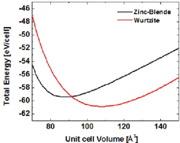
The crystal structure of zinc-IV-nitride semiconductors is expected to be the same as in the III-nitride system, hexagonal wurtzite with space group P63mc. In ZnSnN2, the energetic difference between the wurtzite- and zinc-blende-derived orderings was found to be small (Figure 1.1), suggesting that both phases could coexist under certain growth
Figure 1.1. Energy of wurtzite and zinc-blende structures as a function of unit cell volume. Zinc-IV-nitrides are expected to form with the lower energy wurtzite structure. [1]
4
conditions [3]. However, assuming that the zinc and group IV elements are ordered in the lattice, an orthorhombic symmetry must be used to describe the unit cell instead. A model of the wurtzite structure is depicted in Figure 1.2 alongside the orthorhombic space groups that describe two different high-symmetry arrangements of the cations. Within the c-plane, like-elements can be arranged in rows (Pmc21) or in a zig-zag pattern (Pna21). Most of the theory work assumed the Pna21 space group for their calculations, as it is the most stable [3]. The resulting lattice parameters from the different calculations are shown in Table 1.1.
It should be noted that one study assumed a monoclinic crystal system in calculating their Figure 1.2. Model of the hexagonal wurtzite structure and the two possible ordering of cations in the c-plane. Pna21 is characterized by a zig-zag pattern of like-atoms, and Pmc21 by rows of like-atoms.
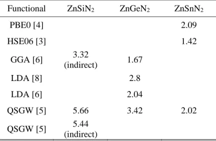
Functional ZnSiN2 ZnGeN2 ZnSnN2
a b c a b c a b c
PBE0 [4] 6.755 5.846 5.473
HSE06 [3] 6.721 5.842 5.459
GGA [5] 6.16 5.41 5.11 6.42 5.54 5.27 6.7 5.8 5.53 GGA [6] 5.279 6.307 5.071 5.535 6.513 5.269
LDA [5] 6.08 5.27 5.02 6.38 5.45 5.22 6.59 5.7 5.41 LDA [6] 5.199 6.182 4.989 5.402 6.351 5.149
LDA-ABINIT
[7] 6.01 5.28 4.98 6.33 5.36 5.11 6.76 5.85 5.58
Functional ZnSiN2 ZnGeN2 ZnSnN2
PBE0 [4] 2.09
HSE06 [3] 1.42
GGA [6] 3.32
(indirect) 1.67
LDA [8] 2.8
LDA [6] 2.04
QSGW [5] 5.66 3.42 2.02
QSGW [5] 5.44 (indirect)
Table 1.1. Theoretical lattice parameters for zinc-IV-nitrides assuming an orthorhombic crystal structure. PBE0 values were converted from calculated monoclinic parameters, and are shown for comparison only. All values are reported in angstroms.
Table 1.2. Theoretical electronic bandgaps for zinc-IV-nitrides. Values are reported in electron volts and represent direct transitions unless otherwise noted.
6 lattice parameters, and the correlating orthorhombic values are shown in Table 1.1 only for comparison [4].
Theoretical electronic band structures were also calculated by various groups.
Because these calculations were heavily dependent on crystal structure data, the bandgap predictions varied widely across the different studies. An example of the calculated band structures for ZnSiN2, ZnGeN2, and ZnSnN2 are shown in Figure 1.3. The plots depicted show that all materials have direct band transitions, although some calculations determined that the lowest energy transition in ZnSiN2 is indirect [5, 6]. Calculated bandgap values are listed in Table 1.2. The range of reported bandgap values spans a large portion of the visible and solar spectra, making this material system attractive for solid state lighting and solar
Figure 1.3. Calculated electronic band structures and density of states for (a) ZnSiN2, (b) ZnGeN2, and (c) ZnSnN2. Data presented here indicates all materials have a direct bandgap. [1]
energy conversion applications. For comparison with the III-nitrides, a plot of theoretical bandgap vs. lattice parameter is shown in Figure 1.4. The accessible bandgap range is somewhat smaller in zinc-IV-nitrides, but the difference in lattice parameters is also smaller, suggesting that alloying and formation of heterostructures will be more straightforward.
Figure 1.4. Theoretical bandgap vs. lattice constant of zinc-IV-nitrides. Known data points for the III-nitrides are included for comparison. The range of lattice constants and bandgaps is smaller for zinc-IV-nitrides. [1]
8
1.2.2 Synthesis
There are many examples in the literature of both ZnSiN2 and ZnGeN2 synthesis. ZnSiN2
powder was synthesized using high-pressure annealing [2], and thin films have been grown on sapphire, (100) silicon, or silicon carbide by metalorganic chemical vapor deposition (MOCVD) [9-12]. More extensive efforts have been put into ZnGeN2 fabrication, leading to powders made by reaction in a furnace [13-15], single crystal rods grown using a vapor- liquid-solid (VLS) method [16], and thin films deposited on glass and silicon by radio frequency (RF) sputter deposition and on sapphire and silicon carbide using MOCVD [9, 17-19]. Alloys of ZnSiN2 and ZnGeN2 have also been deposited by MOCVD [9, 12].
On the other hand, only very recently have reports surfaced of ZnSnN2 synthesis.
Polycrystalline crusts of ZnSnN2 have been formed by a VLS method [20] and thin films were deposited by molecular beam epitaxy (MBE) [21].
1.2.3 Characterization
As with any new material, the first studies of zinc-IV-nitrides focused on characterizing the crystal structure. Drawing from theoretical predictions, the unit cell was expected to be a wurtzite-derived orthorhombic structure. However, various reports disagree about the exact symmetry of these materials. A compilation of experimental lattice parameter measurements are listed in Table 1.3 for the different crystal systems claimed. It should be noted that the difference between the different results is very small, as the monoclinic and orthorhombic crystals are simply slight distortions of the higher symmetry hexagonal
Crystal Structure a b c α β γ
ZnSiN2
Orthorhombic [2] 5.2578(2) 6.3030(3) 5.0287(2) Monoclinic [9] 3.09
Orthorhombic [10] 5.34 6.17 5.04 Orthorhombic [11] 5.05 6.18 5.35
ZnGeN2
Monoclinic [13] 3.157(024) 3.157(024) 5.137(021) 119.5
Hexagonal [14] 3.193 5.187
Orthorhombic [22] 5.454 6.441 5.124
Hexagonal [17] 3.213 5.191
Orthorhombic [18] 5.50(20) 6.44(24) 5.14(25) Hexagonal [19] 3.186(7) 5.174(12)
Monoclinic [23] 3.167 5.194 3.167 118.88
ZnSnN2
Orthorhombic [20] 5.842(7) 6.753(6) 5.462(3)
Monoclinic [24] 3.395 3.4 5.534 89.885 90.033 120.036 Monoclinic [4] 3.375(1) 3.376(1) 5.532(3) 89.98 89.99 119.93 Monoclinic [4] 3.383(4) 3.379(3) 5.567(6) 89.97 89.96 119.95
one. Another important property was measurement of the electronic bandgaps of the different compounds. Experimental estimations of the bandgaps using absorption and photoluminescence are listed in Table 1.4. According to this data, the range of measured ZnGeN2 bandgaps is quite large and there is no consensus on the value of the fundamental bandgap energy.
Additionally, there are a few reports on investigation of the electronic properties of zinc-IV-nitrides. One sample of ZnGeN2 was found to be electrically insulating [17], while another was fairly conductive with a resistivity of 0.3-0.4 Ω∙cm [14]. The discrepancy is
Table 1.3. Experimental lattice parameter measurements for zinc-IV-nitrides.
a, b, and c values are in angstroms, and α, β, and γ values are in degrees.
10 probably due to the difference in synthesis methods for each result. For the conductive material, electron concentrations and mobilities were also reported from Hall effect measurements of 1018-1019 cm-3 and 0.5-5 cm2∙V-1∙s-1 [14]. Similar measurements of
ZnSnN2 films yielded electron concentrations of 1020-1021 cm-3 and mobilities of 10 cm2∙V-1∙s-1 [4]. Studies of phonon modes in ZnSiN2 and ZnGeN2 have also been
conducted using Raman and IR reflection spectroscopies [11, 15, 16, 25].
Reference ZnSiN2 ZnGeN2 ZnSnN2
[2] 3.64
(indirect)
[9] 4.46 3.2
[13] 3.40(1)
[14] 2.67
[15] 3.25
[17] 3.1
[26] 3.3
[27] 2.99(2)
[20] 1.7(1)
[4] 2.12, 2.38
Table 1.4. Experimental electronic bandgap measurements for zinc-IV- nitrides. Values are reported in electron volts and represent direct transitions unless otherwise noted.
1.3 Scope of Thesis
Based on the literature review of zinc-IV-nitride materials, there is certainly room for additional characterization, as the intrinsic properties of the materials are not well understood. For applications in optoelectronic devices, more information about the absorption and electronic properties of ZnSnN2 and ZnGeN2 would also be valuable, since these materials have bandgaps that are useful for interacting with visible light. A majority of the prior research has focused on studying ZnGeN2 for use in optoelectronic devices because of the popularity of its III-nitride analogue, GaN. In this thesis, an emphasis will instead be placed on ZnSnN2 as it is the least studied material with the most promise for visible light applications. Chapter 2 will describe the synthesis of ZnSnN2 by reactive sputtering, for which synthesis had not yet been reported. Chapter 3 will explore tunable bandgap alloys by incorporating germanium to form ZnSnxGe1-xN2. Optical bandgap characterization of various compositions will also be included here. Chapter 4 will discuss the challenges associated with carrier transport measurements, and tie the electronic properties of the materials back to the optical properties. Finally, Chapter 5 will summarize this thesis and identify topics for future work.
12
Chapter 2 Synthesis of Stoichiometric ZnSnN
2At the outset of this project there was no evidence in the literature proving synthesis of ZnSnN2, let alone any experimental characterization of its properties. Because of its predicted bandgap energy of 1.4 to 2 eV [3-5], this material is crucial for implementing the zinc-IV-nitride system of materials into optoelectronic devices that interact with visible light. It was therefore essential that the synthesis of ZnSnN2 be made a priority to begin evaluating the potential of this material system as a whole.
This chapter describes the steps taken towards producing stoichiometric ZnSnN2
by reactive radio frequency (RF) magnetron sputter deposition, a physical vapor deposition technique. Pulsed laser deposition (PLD) was another method used for initial synthesis attempts, but the conditions did not allow for the formation of a homogeneous material (see Appendix). The characterization of the structural properties of the sputter deposited material is also described here, as it was important for demonstrating that the desired material was created. Synthesis of single phase material was confirmed by studies of composition using energy dispersive X-ray spectroscopy (EDXS), and X-ray diffraction (XRD) revealed the wurtzite-derived Pna21 orthorhombic space group with unit cell parameters measured by selected area electron diffraction (SAED). Because of the lack of experimental research in the literature, verification of ZnSnN2 synthesis chiefly relied on
comparison with theoretical predictions of space group and lattice parameters, as well as agreement with the patterns set by experimental work on ZnGeN2 and ZnSiN2. In addition, films were generally oriented with the c-axis perpendicular to the surface of the substrate, and were nearly epitaxial when grown on GaN, highlighting the smaller lattice mismatch compared to sapphire.
2.1 Sputtering Chamber Capabilities
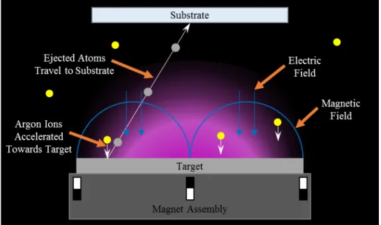
The main advantage of using sputtering to synthesize ZnSnN2 is that a reactive nitrogen source can be produced simply by allowing inert nitrogen gas into the chamber, where interaction with the sputtering plasma causes dissociation of the N2 molecules. A schematic of a typical sputtering chamber is depicted in Figure 2.1. The sputtering process involves accelerating energetic ions towards a target material to eject atoms that then travel to the substrate, as well as the chamber walls. Ions are created by striking a plasma in an inert gas such as argon. These positively charged argon ions (Ar+) are then accelerated towards the target by turning the target material into a negatively charged electrode (cathode). For magnetron sputtering, strong magnets are placed underneath the target in a specific pattern to create a trap for free electrons directly above the target surface, increasing the probability of ionizing neutral argon atoms. Because of the shape of the magnetic field, magnetron sputtering is marked by a circular “racetrack” pattern of erosion on the target. In RF sputtering, the target alternates between acting as a cathode and an anode. The purpose of this is to avoid charge buildup on the target surface, which can occur when DC generators are used on insulating target materials. Even though in this case the targets are metallic and should be able to dissipate any charge buildup, the addition of a reactive gas can potentially
14
alter the composition of the target surface such that it becomes insulating. Reactive gas (typically nitrogen or oxygen) is often introduced in combination with the inert gas because the low atomic weight of the reactive gas alone makes it difficult to efficiently sputter metal targets. Changing the composition of the gas atmosphere in the chamber can also have an effect on the composition and morphology of the deposited film. These processes were all combined in the use of reactive RF magnetron sputtering to synthesize ZnSnN2.
The deposition system used for these studies is an AJA International, Inc. ORION 8 UHV sputtering chamber equipped with seven magnetron sputtering sources, each accommodating target materials that are 2″ in diameter and 0.25″ thick. Each gun is powered by one of three RF generators or two DC generators controlled by a computer interface. The plasma is generally formed in an atmosphere of argon gas, and this system also has nitrogen and oxygen plumbed in for reactive sputtering. The substrate heater can
Figure 2.1. Schematic of reactive RF magnetron sputter deposition. A plasma generates energetic ions (Ar+) that are accelerated towards a target, ejecting atoms that then travel to the substrate.
reach up to 850 °C, and the base pressure in the chamber is on the order of 10-7 Torr, but can be as low as 10-8 Torr after high-temperature baking.
2.2 Achieving Stoichiometric Films
In the initial exploration of ZnSnN2 sputter deposition, it was first important to ensure that the desired stoichiometry could be achieved. Two different methods of deposition were studied: sputtering from a single mixed ZnxSn1-x target and simultaneously sputtering from elemental zinc and tin targets. The procedures for determining the optimal sputtering conditions for each method are discussed here. Tunable deposition parameters included substrate temperature, plasma power, gas pressure, and gas ratio. Film composition was measured using EDXS with an Oxford X-Max SDD system attached to a ZEISS 1550 VP field emission scanning electron microscope (SEM). The accelerating voltage in the SEM was kept at 7-10 kV to constrain the excitation volume to the thickness of the film, which is approximately 200-400 nm.
2.2.1 Sputtering From a Single Mixed Target
Early studies were carried out using a Zn0.50Sn0.50 pressed powder target acquired from ACI Alloys, Inc. with 99.99% purity. This target only allowed for stoichiometric film growth when the substrate temperature was below about 150 °C. At these low temperatures, the surface mobility of the adsorbed atoms is low and the crystalline quality of the film suffers.
However at higher temperatures where the crystalline quality can be improved, the high vapor pressure of zinc leads to a low sticking coefficient and results in zinc-poor films. The
16
zinc desorption at high temperatures can be compensated by a zinc-rich source material, which prompted the use of a Zn0.75Sn0.25 pressed powder target for the remainder of the single target studies.
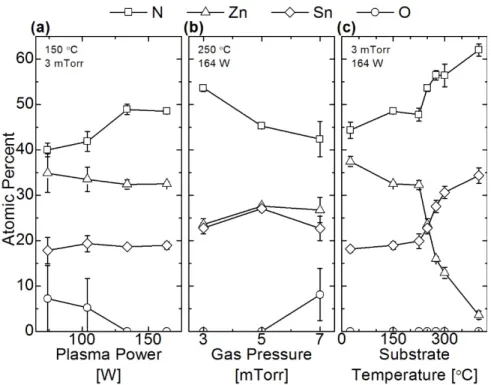
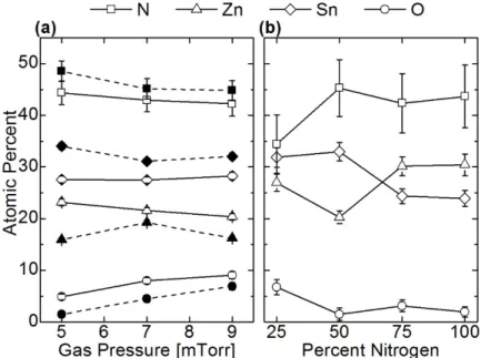
In optimizing the deposition conditions using the Zn0.75Sn0.25 target (99.99%, ACI Alloys, Inc.), it became evident that the first issue needing attention was excess oxygen incorporation in the films during growth. It was important to limit the oxygen to avoid characterization of zinc and tin oxides instead of the desired stoichiometric ZnSnN2. Figure 2.2a-b shows the composition of the films as a function of the plasma power and gas
Figure 2.2. Optimization of deposition parameters when sputtering from a single Zn0.75Sn0.25 target. Composition measured by energy dispersive X-ray spectroscopy from films with varying (a) plasma power, (b) gas pressure, and (c) substrate temperature. Oxygen contamination is reduced in the films when plasma power is high and gas pressure is low. Desired zinc/tin ratio is achieved when the substrate temperature is near 250 °C. All other deposition parameters were held constant as indicated in the top left corner of each panel.
pressure. A significant amount of oxygen is found in films deposited at low plasma powers and high gas pressures. Both of these conditions decrease the deposition rate, which could be as low as 1 nm ∙ min-1 for low powers and only a few nm ∙ h-1 for high pressures. In these instances, the partial pressure of the deposited species is likely on the same order of magnitude as the partial pressure of oxygen in the chamber and both are deposited with comparable rates. Consequently, the combination of high plasma power and low gas pressure gives the lowest oxygen concentration in the resulting films, most likely correlating with an increased deposition rate and decreased relative partial pressure of oxygen. Figure 2.2a-b also shows that when varying the plasma power and gas pressure, there is no significant change in the ratio of zinc to tin, suggesting that the sputtering efficiency of zinc and tin remains proportional under the tested conditions. Additionally, the nitrogen composition appears to be inversely related to the amount of oxygen present in the films such that the oxygen is likely being substituted onto nitrogen sites in the lattice rather than being incorporated interstitially.
To control the zinc/tin ratio, the deposition temperature was varied using 164 W plasma power and a gas pressure of 3 mTorr, which is the best power/pressure combination identified to form a stable plasma and reduce the oxygen as much as possible. As illustrated in Figure 2.2c, the films are highly zinc-rich below 200 °C, at which point a drastic drop in zinc concentration occurs that correlates with the increase in tin and nitrogen atomic percentages. However, the growth window for avoiding excessive zinc desorption is rather small, as above 300 °C the layers become tin-rich. Therefore, the layer stoichiometry is strongly sensitive to the temperature when sputtering from a single mixed target, allowing for a small growth window of about 250 ± 25 °C. Under these conditions, material with the
18 desired stoichiometry for ZnSnN2 could be deposited reliably, but there is little room for variation of the film properties.
2.2.2 Sputtering From Two Elemental Targets
Co-sputtering is a more desirable growth method because it has the advantage of being able to more accurately control the atomic fluxes for each individual metal. In the case of ZnSnN2, the single mixed targets also limited the temperature range for stoichiometric growth. Removing the restriction of a fixed metal ratio could expand this temperature range, which would be useful for altering the film morphology. Another benefit of co-sputtering that was discovered during these investigations is that the rate of
Figure 2.3. Optimization of deposition parameters when co-sputtering from elemental targets. Composition measured by energy dispersive X-ray spectroscopy from films with (a) 60 W zinc plasma power and varying tin plasma power and (b) zinc/tin plasma power ratio of 0.58 and varying the magnitude of the plasma powers. The plasma power ratio for stoichiometric deposition changes as the magnitude of the powers is changed.
sputtering is higher for elemental targets than for mixed targets. The reason for this is unclear, but may be due to changes in bond energy from alloying of zinc and tin or differences in the structure of the targets. The mixed targets are likely porous since they are made from a pressed powder, while the elemental targets are machined from a solid piece of cast metal. An advantageous effect of having a larger sputter yield is that one could expect decreased oxygen incorporation in the film, based on the results from single target sputtering experiments. This allows for the use of lower plasma powers and higher gas pressures, both of which tend to encourage growth of higher quality material. Conversely, adding another variable to the deposition process unfavorably adds to the complexity of the optimization procedure. The elemental zinc and tin targets were acquired from the Kurt J. Lesker Company with 99.99% and 99.999% purity, respectively. In light of the increase in adjustable deposition parameters, the extent of the range of growth options was explored initially. The focus was mainly held on varying the substrate temperature and plasma powers, but alterations in the gas pressure and gas composition were also studied.
First, an appropriate ratio of zinc and tin plasma powers was required that would result in stoichiometric material. Figure 2.3a shows how the composition changes with tin plasma power while the zinc plasma power is held constant at 60 W. All samples were grown at 170 °C in 3 mTorr of a 75% N2 atmosphere, and the tin power was increased until the desired stoichiometry was achieved. For this particular set of samples, the zinc/tin ratio is not exactly 1:1, so the tin power could have been increased even more. Once a ratio of plasma powers was selected for a given substrate temperature, the effect of the magnitude of the power was tested. Composition measurements for samples deposited with a constant zinc/tin plasma power ratio of about 0.58 are shown in Figure 2.3b as a function of the zinc
20
plasma power. With larger plasma powers, the composition is far from stoichiometric even though the ratio of the zinc and tin powers was the same as the other data points. Sputter yields are generally not expected to be linear, making this an unsurprising result, but it does highlight the expanse and complexity of the deposition phase space being explored here.
The next variable tested was the substrate temperature because this parameter was notably restricted in the optimization of single mixed target deposition and could be interesting for altering the film morphology. Samples were deposited with the same zinc/tin plasma power ratio of about 0.58 in 3 mTorr of a 75% nitrogen atmosphere over a range
Figure 2.4. Optimization of deposition parameters when co-sputtering from elemental targets. Composition measured by energy dispersive X-ray spectroscopy from films with (a) 30 W zinc and (b) 44 W zinc as a function of substrate temperature. Open symbols with solid lines indicate a tin plasma power of 44 W, and closed symbols with dashed lines indicate a tin plasma power of 74 W. Films are close to stoichiometric over a large range of substrate temperatures.
of substrate temperatures. The plasma powers included 30 W and 44 W for zinc and 44 W and 74 W for tin. The compositions if these samples are displayed in Figure 2.4a-b as a function of substrate temperature. Surprisingly, the overall results do not appear to change as dramatically as in the single target temperature study. One would expect the zinc content to decrease at higher temperatures due to its high vapor pressure, but near-stoichiometric films were deposited up to about 400 °C. Only for the samples deposited with a tin plasma power of 44 W is the composition significantly far from stoichiometry. This condition occurs at 125 °C for a zinc power of 30 W (Figure 2.4a) and at 250 °C for a zinc power of 44 W (Figure 2.4b). These data points could simply be outliers, so additional replicates of the conditions shown are needed to confirm the results. What this data does show is that it is possible to synthesize near-stoichiometric films over a very wide range of temperatures.
Like the results from the single target studies, changes in the gas pressure did not have a significant effect on the metal composition in the films (Figure 2.5a). Oxygen incorporation still increased with increasing pressure and decreased with an increasing plasma power.
The last parameter tested was the amount of nitrogen present in the atmosphere during deposition. Figure 2.5b shows the composition of films as a function of the percent nitrogen in the argon/nitrogen gas mixture. All samples used 44 W of zinc power, 74 W of tin power, 3mTorr gas pressure, and a substrate temperature of 250 °C. The most obvious result is that the nitrogen content in the film is low when the percent nitrogen in the atmosphere is also low. This can be observed in the sample deposited with 25% nitrogen gas. However, nitrogen is not the only element whose incorporation is affected by a change in the gas composition. The ratio of zinc to tin measured in the films is lower for samples
22 deposited with 25% and 50 % nitrogen compared to the ones deposited with 75% and 100%
nitrogen. This is probably due to the changing mass of the gas mixture and the difference in sputtering efficiency between the two metals. Because tin is a heavier element compared to zinc, it is more efficiently sputtered by the heavier argon ions. When the gas ratio favors argon, more tin will be sputtered and deposited on the substrate, decreasing the zinc/tin ratio in the film. Finally, even though the film composition for samples deposited in 75%
and 100% nitrogen are similar, use of 75% nitrogen was preferred because of the higher deposition rate.
Figure 2.5. Optimization of deposition parameters when co-sputtering from elemental targets. Composition measured by energy dispersive X-ray spectroscopy from films with (a) varying gas pressure and zinc/tin plasma powers of 60/110 W (open symbols) and 120/210 W (closed symbols) and (b) varying nitrogen content in the chamber atmosphere. Gas pressure only appears to affect oxygen incorporation, and is decreased at higher plasma powers. Low nitrogen gas content results in decreased nitrogen in the film and increased sputtering of tin.
2.3 Characterization of the Crystal Structure
Composition measurements alone could not ensure that the deposited films consisted of a phase-pure compound semiconductor material. For example, the material could have been made up of domains of zinc, tin, or the nitrides or oxides of those elements. To prove that the deposited material is in fact the correct phase of ZnSnN2, the crystal structure of the films was characterized in addition to measuring the stoichiometric composition. Powder XRD measurements indicated that the material is crystalline with a wurtzite-derived unit cell, confirming the theoretical calculations for ZnSnN2 [3, 5, 7]. Additionally, the lattice parameters within the unit cell, which are important for material identification, were measured by XRD and SAED of the deposited films.
2.3.1 Space Group
Powder diffraction patterns were measured from a ground up thick film that was removed from the substrate to determine the phase of the sputtered material. The position and relative intensity of peaks in a powder diffractogram are a type of “fingerprint”
allowing identification of distinct materials, where each peak represents a spacing between atomic planes within the unit cell of the crystal. The assumption made in this measurement is that the particles in the powder are sufficiently small and randomly oriented such that all interplanar spacings of the unit cell are represented. Measurements were made using a PANalytical X’Pert Pro powder diffractometer over a 2θ range of 20° to 80°. The X-rays are generated with a Cu Kα source, which creates photons with a wavelength of about 1.54 Å.
24
To prepare powder samples for measurement, an alumina mortar and pestle was used to grind ZnSnN2 films adhered to sapphire substrates. The films were on the order of 102 nm thick while the substrate thickness was 0.5 mm or 0.1 mm. For both substrate thicknesses, the strong diffraction from the single crystal sapphire obscured the measurement of peaks corresponding to the film. Making a film that is thicker than the substrate was not feasible, as it would require 400-500 h of deposition time to reach a suitable thickness. Instead, a film was deposited on a 2″ sapphire wafer to a thickness of a few μm and removed from the substrate by rapid thermal annealing (RTA). The sample was ramped up to 600 °C over 30 s and held at that temperature for 60 s before passively cooling back to room temperature. Because of the large difference in thermal expansion coefficient between ZnSnN2 and sapphire, the film cracks and flakes off of the substrate
Figure 2.6. Powder diffraction spectrum of ZnSnN2 measured by X-ray diffraction. Peak positions are also shown that were calculated from theoretical zero Kelvin lattice parameters for the Pmc21, Pna21, and average wurtzite structures.
Pmc21 and Pna21 are both ordered orthorhombic unit cells, and the average wurtzite unit cell assumes random ordering of zinc and tin atoms.
under the thermal stress. The flakes were then collected and ground into a fine powder using the mortar and pestle.
The measured powder diffractrogram is shown in Figure 2.6. Theoretical peak positions based on calculated zero Kelvin lattice parameters [3] for Pna21, Pmc21, and an average wurtzite structure, representing a random distribution of zinc and tin atoms, are shown for comparison. The measured pattern matches well with the Pna21 and average wurtzite structures, where the most apparent distinguishing feature is a slight splitting of some peaks in the Pna21 structure. Although it appears that the ZnSnN2 diffraction pattern does not contain split peaks, it should be noted that the full width at half maximum (FWHM) of the peaks that would be split in the Pna21 case is large compared to the peaks that are not expected to be split. This suggests that the Pna21 space group describes the predominant arrangement of metallic atoms in the measured sample. This is consistent with reports on synthesis of ZnGeN2 and ZnSiN2 materials, where several groups have shown that they both exhibit the Pna21 structure [2, 15, 18, 22, 28]. Another important piece of evidence to point out is that the peaks present in the samples do not match with the diffraction patterns for Zn or Sn metals, nor with the patterns of the oxides or nitrides of those elements. This further supports the claim that the material being created and characterized is in fact ZnSnN2.
2.3.2 Lattice Parameter Measurements
After determining that the space group is orthorhombic, the lattice parameters can be accurately measured by using different diffraction techniques. The powder diffraction data shown in Figure 2.6 was not suitable for making these measurements since there was no
26 internal standard included in the powder sample to calibrate the peak positions. Instead, XRD measurements of films on the substrate were made with the system aligned to the substrate peak. The disadvantage of using this method is that only the atomic planes that are parallel to the surface of the substrate can be observed. In addition, SAED patterns were measured in a transmission electron microscope (TEM) to gain information about interplanar distances in other directions.
The majority of the crystalline ZnSnN2 films deposited on sapphire or GaN were oriented with the c-axis perpendicular to the plane of the substrate. This allowed for the measurement of the c lattice constant using θ-2θ XRD and Bragg’s Law given in Equation (2.1), where dhkl is the distance between (hkl) planes, n is a positive integer, λ is the wavelength of the incident X-rays, and θhkl is the angle between incoming X-rays and the surface of the crystal that results in diffraction from (hkl) planes:
𝑑𝑑ℎ𝑘𝑘𝑘𝑘 = 𝑛𝑛𝑛𝑛
2 sin 𝜃𝜃ℎ𝑘𝑘𝑘𝑘 . (2.1)
Since the (hkl) plane being observed in the ZnSnN2 films is the (002) plane, the calculated interplanar spacing is equal to half of the c lattice constant. θ-2θ XRD measurements were made using a PANalytical X’Pert Pro MRD over a 2θ range of 25° to 45° and aligned to the sapphire (0006) peak. The average 2θ peak position of (002) planes for a number of films on sapphire was about 32.4°, corresponding to a c lattice constant of 5.52 ± 0.01 Å.
To measure the a and b lattice constants, SAED patterns were imaged on a CCD camera using an FEI Tecnai TF30 TEM operated at 300 kV. A double-tilt sample holder was used in the microscope to more easily align the electron beam to the zone axis of the substrate. Due to the use of electromagnetic lenses in the microscope, the camera length
does not represent a fixed physical length and requires calibration before analyzing the film.
This was done by measuring known diffraction spots in the images. In this case, SAED patterns were taken of the substrate alone using the same camera length setting as for the film and the actual camera length, L, was calculated by
𝐿𝐿 = 𝑅𝑅ℎ𝑘𝑘𝑘𝑘𝑑𝑑ℎ𝑘𝑘𝑘𝑘
𝑛𝑛 , (2.2)
where Rhkl is the distance between the transmitted and (hkl) diffracted beams in the SAED image, dhkl is the distance between (hkl) planes, and λ is the wavelength of the electrons (about 1.97 pm for 300 kV electrons). Known substrate lattice parameters used for the calculations were a = 4.759 Å and c = 12.992 Å for sapphire, and a = 3.189 Å and c = 5.185 Å for GaN. The camera length was calibrated to be 740 mm for the sample on sapphire and 392 mm for the sample on GaN. The difference between the two is only due to changes in the microscope settings.
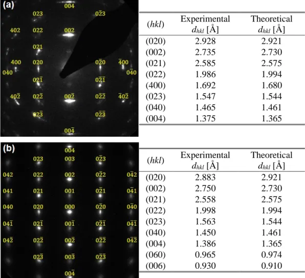
To measure the lattice parameters, the diffraction spots in the SAED patterns of ZnSnN2 films needed to be indexed. These indexed patterns are displayed in Figure 2.7a- b for ZnSnN2 on both substrates. The procedure for indexing is similar to calibrating the camera length, only in reverse. Equation (2.2) can be rearranged so that L, λ, and Rhkl are used to calculate dhkl for each diffraction spot. Calculated dhkl spacings based on measured Rhkl values are listed in Figure 2.7a-b for both patterns. The interplanar distances were then compared to values derived from theoretically calculated lattice constants [3] to assign a Miller index, (hkl), to each diffraction spot. The theoretical dhkl values corresponding to the measured spots are also included in Figure 2.7a-b for comparison. Lattice constants were then calculated from the dhkl of planes perpendicular to the unit cell faces, i.e. (100), (010),
28
(hkl) Experimental dhkl [Å]
Theoretical dhkl [Å]
(020) 2.928 2.921
(002) 2.735 2.730
(021) 2.585 2.575
(022) 1.986 1.994
(400) 1.692 1.680
(023) 1.547 1.544
(040) 1.465 1.461
(004) 1.375 1.365
(hkl) Experimental dhkl [Å]
Theoretical dhkl [Å]
(020) 2.883 2.921
(002) 2.750 2.730
(021) 2.558 2.575
(022) 1.998 1.994
(023) 1.563 1.544
(040) 1.450 1.461
(004) 1.386 1.365
(060) 0.965 0.974
(006) 0.930 0.910
Figure 2.7. Indexed selected area electron diffraction patterns for ZnSnN2 films on (a) c-sapphire and (b) c-GaN substrates. Tables present experimental interplanar lattice spacings, dhkl, calculated from measured distances between spots in the diffraction patterns. Miller indices, (hkl), were assigned by comparing experimental and theoretical interplanar distances [3].
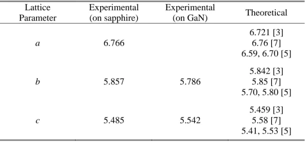
and (001). On sapphire, the measured ZnSnN2 lattice constants are a = 6.766 Å, b = 5.857 Å, and c = 5.485 Å. Measurement of both the a and b constants was only possible because the grains in the film on sapphire were oriented in multiple planar directions. On GaN, the a lattice constant was not measureable because the grains were mostly oriented in the same direction, with the (100) planes perpendicular to the electron beam. However, the other constants were measured to be b = 5.786 Å and c = 5.542 Å. Table 2.1 also presents theoretical lattice constants for comparison.
In the case of ZnSnN2 on sapphire, the measured lattice constants agree fairly well with the theoretical zero Kelvin lattice constants [3], with each one differing by less than 1% from the theory. Some disagreement is expected because the measurements were made at room temperature, where thermal energy would cause an expansion of the zero Kelvin unit cell, and in fact the measured values are all larger than the theoretical constants. The film on GaN, however, deviates more from the theoretical values with differences of -1%
and 1.5% for the b and c parameters, respectively. One possible explanation for this is that the ZnSnN2 film was strained to the GaN lattice, while the sapphire lattice mismatch was so large that the ZnSnN2 grew as a relaxed film. For comparison, if the hexagonal wurtzite lattice were described by a Pna21 unit cell instead, its “b” lattice constant would be equal to 𝑎𝑎ℎ∙ √3, where ah is the a constant in the hexagonal unit cell. These “b” values are 5.524 Å for GaN and 8.243 Å for sapphire. The fact that the measured b parameter is smaller than the predicted value for ZnSnN2 on GaN supports the hypothesis that the film is strained, as the ZnSnN2 unit cell would be required to compress in the b direction to align with the GaN lattice.
30
Lattice Parameter
Experimental (on sapphire)
Experimental
(on GaN) Theoretical
a 6.766
6.721 [3]
6.76 [7]
6.59, 6.70 [5]
b 5.857 5.786
5.842 [3]
5.85 [7]
5.70, 5.80 [5]
c 5.485 5.542
5.459 [3]
5.58 [7]
5.41, 5.53 [5]
2.4 Film Structure and Morphology
From the previously discussed composition and crystal structure measurements, it was reasonably clear that single phase ZnSnN2 could be synthesized. The next task was to study the morphology of the films and see how the deposition conditions affected the structure.
θ-2θ XRD measurements of films on their substrates were used for these studies, which only allow for observation of atomic planes that are parallel to the surface of the substrate.
The majority of the deposited ZnSnN2 films on c-sapphire and c-GaN substrates were oriented such that the (002) reflection peak was the only one visible. Observation of other orientations indicated a highly polycrystalline material without any relationship to the substrate.
A major issue was encountered when attempting to quantify the effect of varying deposition conditions on the structure of the films. For material grown on c-sapphire
Table 2.1. Measured ZnSnN2 lattice constants. Values were derived from measured (100), (010), and (001) interplanar distances. Theoretical lattice constants are also included for comparison. All numbers are reported in angstroms.
substrates, the (002) peak was not consistently observed in films deposited under the same conditions. It is still unclear what factors were ultimately hindering the reproducibility of the deposited film structure. One possible reason is related to the volatility of zinc. During these experiments, co-sputtered ZnSnN2 films deposited consecutively under the same conditions were observed in XRD to have (002) peaks that decreased in intensity and eventually disappeared. Zinc also appeared to accumulate in the vacuum chamber, manifesting as an increase in zinc content for films deposited later in the series. It is therefore possible that excess zinc left in the chamber interferes with nucleation or deposition of subsequent material.
Whatever the origin for this lack of reproducibility, it turned out not to affect the crystallinity of films deposited on c-GaN substrates. This is probably a result of the smaller lattice mismatch between ZnSnN2 and GaN, compared to that of ZnSnN2 and sapphire, making it easier to form crystalline material when the conditions are not perfect. Figure 2.8 shows θ-2θ XRD measurements from stoichiometric ZnSnN2 films deposited together on
Figure 2.8. θ-2θ X-ray diffraction data from stoichiometric ZnSnN2 films deposited at the same time on c-sapphire and c-GaN substrates, meaning deposition conditions were exactly the same. Crystalline film was able to grow on GaN, but an unknown factor hindered high quality growth on sapphire.
32
Figure 2.9. θ-2θ X-ray diffraction data from ZnSnN2 films deposited with 60 W zinc plasma power and varying tin plasma power. (002) peak loses intensity and broadens as the tin power is decreased and film composition deviates further away from stoichiometry (Figure 2.3a).
Figure 2.10. θ-2θ X-ray diffraction data from ZnSnN2 films with varying gas pressure and zinc/tin plasma powers of (a) 60/110 W and (b) 120/210 W. (002) peak loses intensity and broadens as gas pressure is increased. Deposition using higher power results in mostly amorphous material.
c-sapphire and c-GaN, meaning all of the deposition conditions were exactly the same. The film on c-GaN is crystalline and textured with a very sharp (002) peak around 32.4°, while the film on c-sapphire is amorphous or possibly nanocrystalline. As a result, a few studies were carried out to examine the structural effect of varying deposition conditions using only c-GaN substrates. XRD measurements from the same samples examined in Figure 2.3a are shown in Figure 2.9. As the film composition moves further away from stoichiometry, the (002) peak loses intensity and broadens, indicating that the material structure is becoming increasingly disordered. Similarly, XRD from the samples examined in Figure 2.5a are shown in Figure 2.10a-b. For films deposited with 60 W zinc plasma power, the (002) peak loses intensity and broadens as the gas pressure is increased.
Figure 2.11. Transmission electron microscope bright field image of ZnSnN2 on c-sapphire substrate viewed in cross-section. Grains are columnar and less than 50 nm wide, which is typical for sputtered material.
34
The resulting increase in oxygen incorporation in the films likely forms an abundance of defects in the crystal structure, which causes the change in the peak shape. When the power is increased to 120 W zinc plasma power, the XRD measurements reveal that the material is mostly amorphous, even though the oxygen content is lower in these films. The higher plasma power may cause the substrate and growing film to be bombarded by higher energy sputtered molecules that can disrupt the crystal structure.
Transmission electron microscopy was also used to study the morphology of the films. Figure 2.11 shows a TEM bright field image of a cross-sectional sample of ZnSnN2
deposited on a c-sapphire substrate. The film clearly consists of columnar grains that are less than 50 nm wide. The grain size also appears to increase towards the surface of the film as grains coalesce during growth. SAED from the same film’s interface (Figure 2.12a)
Figure 2.12. Selected area electron diffraction patterns from the interface of ZnSnN2 films on (a) c-sapphire and (b) c-GaN substrates. Diffraction spots indicate that the c-plane in ZnSnN2 is aligned to the c-plane of sapphire and of GaN.
Additionally, (1010) substrate planes are aligned with (100) and (010) ZnSnN2
planes on sapphire and only with (010) ZnSnN2 planes on GaN. Miller indices in yellow belong to ZnSnN2 and indices in blue belong to the substrate.
shows that the grains are aligned with the substrate such that either the (010) or (100) atomic planes are parallel with the (1010) plane in the sapphire. This indicates that some grains are rotated 90° from each other in the plane of the substrate. In contrast, the SAED from a film grown on a c-GaN substrate shows only one in-plane direction for the ZnSnN2
grains (Figure 2.12b). These results again reinforce the conclusion that higher quality ZnSnN2 is grown on GaN because of the smaller lattice match.
2.5 Conclusion
Presented in this chapter is the optimization of deposition parameters to achieve single phase ZnSnN2, a new earth-abundant semiconductor. This compound is important for demonstrating the applicability of the entire zinc-IV-nitride material system in visible light optoelectronic devices. Furthermore, ZnSnN2 was able to be synthesized using a cost- effective and scalable deposition method, strengthening its potential for large-scale device applications.
Stoichiometric single phase ZnSnN2 was synthesized using reactive RF magnetron sputter deposition from a single mixed ZnxSn1-x target or from elemental zinc and tin targets.
Co-sputtering provides for an expansive array of variable deposition parameters, of which only a small portion has been explored here. EDXS composition measurements were used to optimize the deposition conditions for reducing oxygen contamination and achieving a zinc/tin ratio of close to 1 in the deposited film. The material exhibited the predicted Pna21
wurtzite-derived orthorhombic crystal structure with lattice parameters measured from SAED patterns that agree with theoretical values. The morphology of the films was also studied using XRD and TEM. Grains are columnar and small, less than 50 nm, which is
36 typical of sputtered material. The choice of substrate also played a large role in making high quality material. The smaller lattice mismatch to GaN, compared to sapphire, allowed for growth of highly crystalline and textured ZnSnN2 films that were strained at the interface to match with the lattice of the substrate.
In the next chapter, exploration of the zinc-IV-nitride material system will be extended by alloying ZnSnN2 with ZnGeN2, resulting in an earth-abundant tunable bandgap semiconductor that spans a majority of the visible spectrum. Optical properties of these alloys will be characterized to determine if they can potentially serve as an alternative to InxGa1-xN in optoelectronic devices.
Chapter 3 Tunable Bandgap ZnSn
xGe
1-xN
2Alloys
In recent years, InxGa1-xN alloys have attracted attention in the scientific community because of their demonstrated success in optoelectronic devices, especially those that interact with visible light such as light-emitting diodes (LEDs) and photovoltaics. For such applications, InxGa1-xN is ideal because the direct bandgap is tunable over a theoretical range of 0.7 eV to 3.4 eV by changing the amount of indium in the alloy, and high quality material can be grown with large absorption coefficients and mobilities. However, InxGa1-xN alloys with high indium content have been difficult to grow because InN and GaN have a large difference in lattice parameters, leading to indium segregation and phase separation. Extensive research has been conducted in pursuit of overcoming this problem so that the entire theoretical bandgap range can be accessed. Incorporating more than about 30% indium into the alloy results in phase separation, which limits the bandgap to the blue range of the visible spectrum. This is generally referred to as the “green gap” in the LED industry, as researchers have been unable to produce an efficient green LED that emits between 520 and 530 nm. Even though there are more sophisticated growth strategies for InxGa1-xN that allow for near-green emission, such as quantum well structures, the scarcity and cost of indium will limit its large-scale deployment.
38 Based on theoretical predictions, earth-abundant ZnSnxGe1-xN2 is expected to have similar optical and electronic properties to InxGa1-xN [7], and can potentially be tuned to span an energy range of 1.4 eV to 2.9 eV, which still covers the majority of the visible spectrum. Although the alloy has a shorter range of predicted bandgaps, it also has a smaller lattice mismatch between its constituent materials, ZnSnN2 and ZnGeN2. This is a potential advantage for alloying because the large lattice mismatch is a major factor contributing to the phase separation of InN and GaN. If phase separation does not occur, ZnSnxGe1-xN2
could be capable of closing the “green gap.” Additionally, an efficient graded or multi- junction photovoltaic device could be developed with any combination of bandgaps between 1.4 eV to 2.9 eV. One simply needs to search the literature for InxGa1-xN to have an idea of the range of optoelectronic devices that could benefit from an earth-abundant alternative.
In this chapter, ZnSnxGe1-xN2 is synthesized by adding germanium to the sputtering process described in Chapter 2. A wide range of compositions with the correct zinc and nitrogen stoichiometry can be accessed using this method. X-ray diffraction (XRD) measurements show a linearly shifting (002) peak, indicating no phase separation.
Spectroscopic ellipsometry reveals optical bandgaps that increase with increasing germanium incorporation from about 1.8 to 3.1 eV.
3.1 Linear Incorporation of Germanium to Form ZnSn
xGe
1-xN
2ZnSnxGe1-xN2 thin films were deposited on c-sapphire and c-GaN substrates by reactive radio frequency (RF) co-sputtering from metal targets in an argon/nitrogen plasma. The
gas pressure was held at 3 mTorr during deposition with 75% nitrogen in the plasma. To encourage crystalline growth, the substrate temperature was set to about 270 °C. For ZnSnxGe1-xN2 with x = 0 or 1, films were deposited by co-sputtering from zinc (99.99%) and germanium (99.999%) or zinc and tin (99.999%) elemental targets, all obtained from the Kurt J. Lesker Company. An RF power of 44 W was applied to the zinc target, while the tin and germanium targets required 74 W and 104 W, respectively, to obtain stoichiometric films as determined by energy dispersive X-ray spectroscopy (EDXS).
Films with 0 < x < 1 were sputtered from a Zn0.75Sn0.25 pressed powder target (99.99%, ACI Alloys, Inc.) and a germanium elemental target because the sputtering system was limited to two RF power supplies at the time of these experiments. The combined target is zinc-rich because the high vapor pressure of zinc limits its incorporation during deposition at substrate temperatures above about 200 °C (see Chapter 2). For the data presented here, the RF power on the Zn0.75Sn0.25 target was kept at 134 W and the power applied to the germanium target was varied from 30 W to 134 W to create a set of samples with ranging compositions. As shown in Chapter 2, the combined target requires a higher power than the elemental targets to get a comparable deposition rate that limits oxygen incorporation in the film.
3.1.1 Measurements of Composition Variation
Figure 3.1 presents the composition measurements for ZnSnxGe1-xN2 films on c-sapphire and c-GaN substrates using EDXS. An accelerating voltage of less than 10 kV was used to confine the size of the activation volume to the thickness of the thin films. All of the samples have close to 25 at% zinc and 50 at% nitrogen within error. The quaternary films
40
on c-sapphire have x values of 0.71 ± 0.07, 0.51 ± 0.06, 0.40 ± 0.05, and 0.37 ± 0.04, corresponding to germanium RF powers of 44 W, 74 W, 104 W, and 134 W, respectively.
The films on c-GaN have x values of 0.88 ± 0.03, 0.81 ± 0.02, 0.61 ± 0.02, 0.50 ± 0.02, and 0.36 ± 0.01, corresponding to germanium RF powers of 30 W, 44 W, 60 W, 104 W, and 134 W, respectively. The value of x was calculated by taking the ratio of atomic percent tin to the total atomic percent of group IV elements.
Figure 3.1. Composition of ZnSnxGe1-xN2 films deposited on (a) c-sapphire and (b) c-GaN substrates measured by energy dispersive X-ray spectroscopy. Films on each substrate exhibit consistent zinc and nitrogen concentrations close to 25 at%
and 50 at%, respectively. Various tin and germanium concentrations are demonstrated, allowing for characterization of a wide range of alloy compositions.