First of all, I would like to acknowledge the guidance, support and patience of my advisor, Prof. William Jemison. I would like to thank him for introducing me to the world of microwave technology.
Applications of High-Efficiency L-Band Amplifiers
Cellular Applications
PA headphones typically have a peak power output ranging from one watt to several watts. Most headphone PAs are built on-chip as integrated circuits with few off-chip components.
Radar Applications
Organization of Thesis
Rutledge, “Bifurcation analysis of stabilization circuits in an L-band LDMOS 60-W power amplifier,” IEEE Microwave Wireless Compon. Rutledge, "Current Status of the High-Efficiency L-Band Transmit/Receive Module Development for SAR Systems," NASA 2003 Earth-Sun Syst.
High-Efficiency Design Techniques
Transconductance Amplifiers
- Class-A Amplifiers
- Class-AB, Class-B, and Class-C Amplifiers
This is the reason why Class-A amplifiers are not suitable for L-band high power amplifiers. The ideal maximum drain efficiency of a Class-B amplifier is 78.5%, which is significantly higher than the Class-A amplifier.
Switching Amplifiers
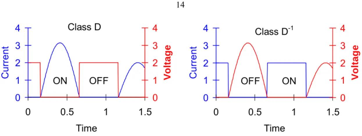
- Class-D and Class-D -1 Amplifiers
- Class-E Amplifiers
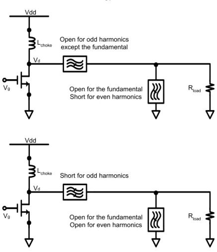
- Class-F and Class-F -1 Amplifiers
- Class-E/F Family
However, one of the assumptions for Class-D and Class-D-1 amplifiers is that the transistors have zero output capacitance. Also, the efficiency of the amplifier is significantly reduced as the output capacitance of the transistor becomes large.
L-Band Implementation of Class-E/F Amplifiers
- Transistor Output Capacitance and the Second Harmonic Trap
- Loss Mechanisms in Power Amplifiers
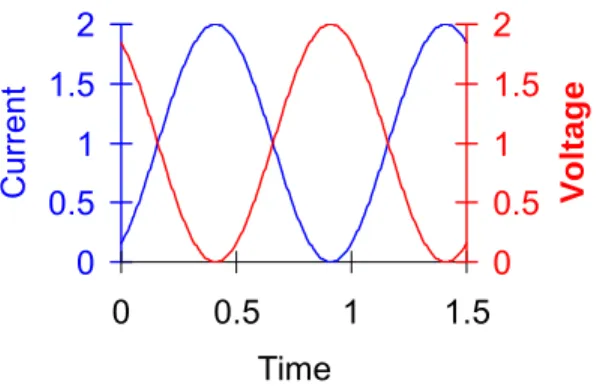
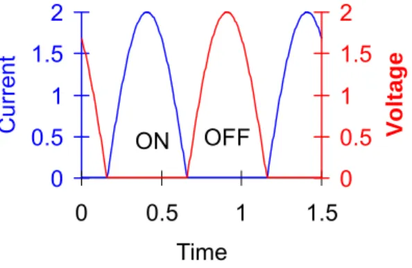
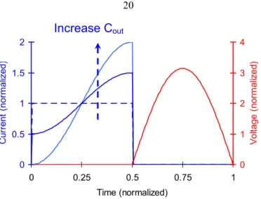
Change in current waveform due to change in output capacitance of transistors in class E/Fodd amplifiers. The main loss mechanisms due to active devices include forwarding loss, discharge loss, and matching loss.
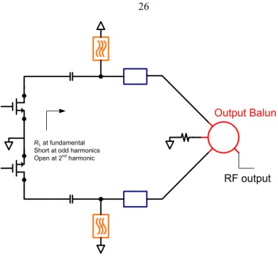
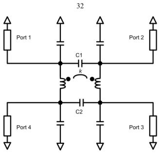
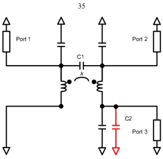
Transformers, Baluns, and Power-Combining Technologies
Baluns in Power Amplifiers
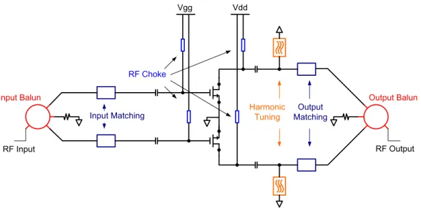
At the input and output of the amplifier there are two 50 Ω stand-alone baluns. In fact, two identical 50 Ω baluns can be used at the input and output of the amplifier.
Examples of Transformers and Baluns
- HF, VHF, and UHF Transformers
- Microwave Baluns and Transformers
- Distributed Active Transformer (DAT)
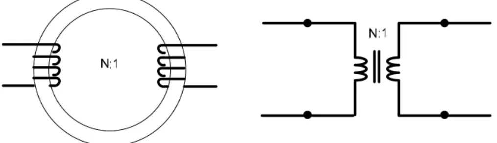
The advantage of the balun is that it can achieve balanced outputs with relatively simple implementation for an octave bandwidth. While all of the microwave baluns shown can be implemented in L-band discrete power amplifiers, the size of the baluns is too large for this frequency band.
Compact L-Band Baluns
- Lumped-Element Model
- Tight-Coupling Microstrip Lines
- Balance Optimization
- Input Impedance Transformation
- Output Impedance Transformation
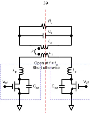
- Center-Tapped DC Feed and 2nd Harmonic Trap
Since one end of the inductor shown in Figure 3.13 is grounded (let port 4 be grounded in this case), the equivalent circuit is modified as Figure 3.18. Since the input and the output of the RF power devices typically have low impedances, impedance matching is critical. The design of the impedance-transforming balun is based on the simplified equivalent circuit model of the balun shown in Figure 3.13.
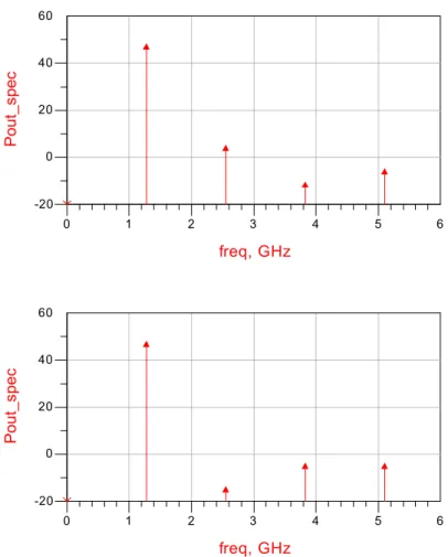
However, simulation tools can also be used to optimize the values of inductances and capacitances. In low-frequency power amplifiers, it is common to feed DC power to a push-pull amplifier at a symmetry point of the amplifier as shown in Figure 3.24. In Figure 3.27, we see a comparison of the simulated output spectrum before and after applying the second harmonic trap.
Simulation of the 2nd harmonic trap in the Smith chart showing an open circuit for the 2nd harmonic.
Balun Selection
- Bandwidth
- Size
- Impedance Level and Impedance Transformation
Coil transformers and transmission line transformers are among the widest bandwidth baluns that can be used in these types of applications. As amplifier designers, we typically want compact baluns to reduce the overall size of the amplifier. From this perspective, most baluns belong to one of the following two cases: (1) the size of the balun is much less than a quarter wavelength, and (2) the size is comparable to a quarter wavelength.
In these baluns, the lengths of the transmission lines are much less than a quarter wavelength (typically less than a sixth of a quarter wavelength), and can therefore be assumed to be coupled inductors. It is important to consider the impedance level of the components, realizable in a particular processing technology. For example, if a coaxial cable is used as part of the balun, and the impedance of the transistor is 10 Ω, the characteristic impedance of the coaxial cable must be between 10 Ω and 50 Ω.
For the same transistor technology, if coupled coils are used in the balun, the reactance of the inductor must be between 10 Ω and 50 Ω.
Implementation of Power Amplifiers
Implementation and Measurement
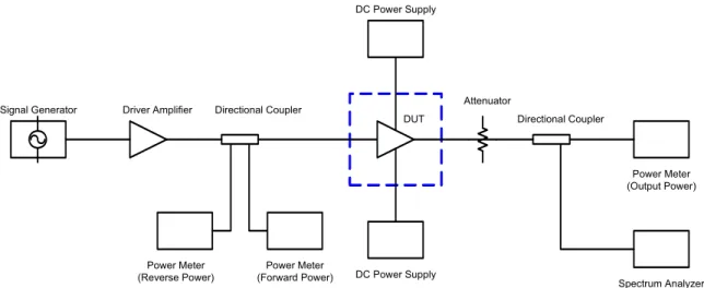
The width of the fingers is 20 mils while the spacing between the fingers is 5 mils. The measurement block diagram is shown in Figure 4.2, and a photograph of the measurement setup is shown in Figure 4.3. One way to increase the operating frequency is to reduce the self-inductance of the output balun.
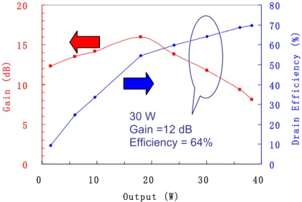
The first change to the amplifier is to allow the drains of the transistors to connect to each other. Using this layout, the lengths of the baluns are significantly reduced from the previous design. The output power spectrum of the amplifier shows excellent suppression of harmonics of the fundamental frequency.
The circuit diagram is shown in figure 4.14, and the picture of the amplifier is shown in figure 4.15.
Performance Comparison
Bifurcation Stability Analysis of L-Band Power Amplifier
Introduction to Stability Analysis
- Methods in Stability Analysis
In the case of push-pull amplifiers, linear techniques do not provide information about the amplitude and phase of the oscillation. This technique takes into account the nonlinear elements in power amplifiers and accurately predicts the conditions for the oscillations to occur. Stability circuits focus on the interaction of the source and load impedances with the input and output impedances of the amplifier.
Practically, a variety of stability circles can be drawn by sweeping the frequency and the bias conditions of the amplifier. The amplitude and the phase of the oscillation provide useful information about the nature of the oscillation. The analysis does not require accurate nonlinear models of the active devices, which are often difficult to find.
In the simplest case, where a circuit contains only passive merged elements, the stability conditions can be discussed using the solutions of the following differential equation.
Nonlinear Bifurcation Analysis
- Oscillation Detection Using Small-Signal Generator
- Determination of Stability Contour
- Bifurcation Analysis Using Auxiliary Generator
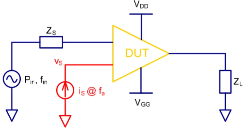
The vectors of the state variables, the nonlinear elements, and the independent generators are represented by . Conversion matrix approach to detect oscillations using a small-signal current source inserted in a node of the power amplifier. The poles and zeros of the impedance function Z can be plotted on the complex plane.
However, the two sets of unstable poles are canceled by the two sets of unstable zeros of the admittance function. Two important pieces of information contained in a large signal source are the amplitude and the phase of the signal. The undisturbed condition is solved to determine the amplitude and phase of the oscillation.
The output of the phase information is shown later in the chapter.
Application to L-Band Power Amplifier
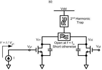
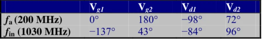
The phase information is used to determine whether the oscillation is in the even mode or in the odd mode. During the operation of the Class E/F amplifier, low frequency oscillations are observed around 200 MHz. This oscillation is only achieved at a certain combination of input power, drive frequency, and drain and gate biases.
The oscillation and driving frequency are 1030 MHz, where the input power and gate bias are fixed. As the drain voltage increases, the low frequency oscillation is observed when the drain bias is 4.5 V. For fin > 1.14 GHz, no instability is obtained at any of the considered biases.
Boundaries between stable and unstable regions based on global amplifier stability analysis, for different operating conditions.
Stabilization Techniques
- Stabilization with an Odd-Mode Stabilization Resistor
- Stabilization with Neutralization Capacitors
- Stabilization with Feedback Resistors
- Comparison of Performance
The odd-mode oscillation can be eliminated by connecting a resistor between the gate terminals of the two transistors, shown in Figure 5.13. Using the half-circuit analysis for the odd-mode oscillation at 200 MHz, the stabilizing resistor is parallel to the gate of the transistors, shunting the oscillation signal to ground. The maximum allowable value for the stabilization resistance R is obtained by following the oscillation limit in the plane defined by R and one of the four circuit parameters.
When stabilizing resistors are implemented, the curves shift to the right side of the complex plane. In push-pull configurations, neutralization capacitors can be connected between the gate and drain terminals of the opposite transistors to cancel unwanted feedback through Cgd. To reduce the positive feedback, a resistor and a DC-blocking capacitor are connected between the gate and drain terminals of the same transistor, shown in Figure 5.18.
The neutralization capacitors improve the amplifier's gain by about 2 dB, but the PAE is reduced by 6%.
Summary
Future Opportunities
New Transistor Technologies
- Si and GaAs Devices
- SiC and GaN Devices
- SiC Class-E Power Amplifier
Traditionally, the operating frequency of a switching power amplifier is limited by the output capacitance of the device. They also limit the bandwidth and increase the complexity and size of the power amplifier. The property of low output capacitance can greatly simplify the output matching circuit and improve the efficiency of the power amplifier.
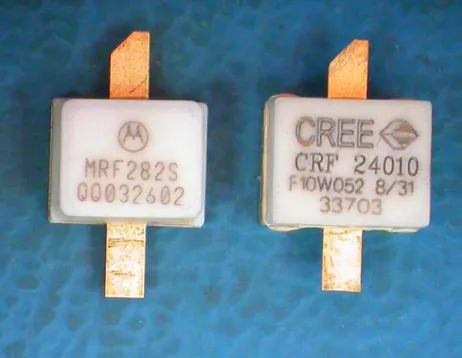
The measured input and output impedance (provided by Cree) of the SiC MESFET are shown in Figure 6.2. The output power is not nearly as high as that of the most modern LDMOS and GaAs power devices, which can deliver more than 200 W. HEMT shares some of the problems with SiC devices, such as the lack of large signal models and reliability issues.
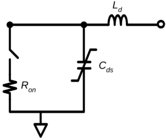
A DC measurement of the device is taken and the on-resistance is extracted from the DC curves.
Modeling for Switching-Mode Amplifiers
The difficulty with this method is that measuring the output capacitance is difficult. At this frequency, it is difficult to separate the measurement of the output capacitance Cds from the feedback capacitance Cdg. It is necessary to come up with a set of simple measurements and extract the critical non-linear elements of the transistor model and optimize the amplifier waveforms based on the corresponding circuit model shown in Figure 6.7.
The on-resistance of the power supply device is an important property of switching power amplifiers. The resistive dissipation of the power amplifier is directly related to the on-resistance of the power amplifier. The on resistance can be determined by measuring the DC IV characteristics of the device.
The non-linearity of the capacitance can be modeled by fitting a curve to a range of bias conditions.
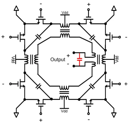
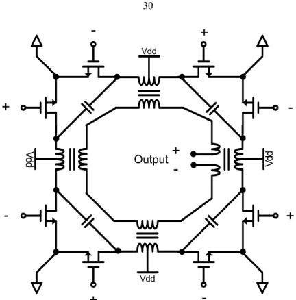
Discrete L-Band DAT
- Challenges in Discrete L-band DAT
- Layout and Simulation
Joshin, “A GaN HEMT push-pull amplifier with over 200W output power and high reliability,” IEEE MTT-S Int. 200W Push-Pull and 110W Single-Ended High-Performance RF-LDMOS Transistors for WCDMA Base Station Applications”, IEEE MTT-S Int. Fukaya, “An ultra-wide band 300 W GaAs power FET for W-CDMA base stations,” IEEE MTT-S Int.
Kim, “High efficiency power amplifier for CDMA base stations using Doherty configuration,” IEEE MTT-S Int. Kenney, “Closed-Loop Digital Predistortion for Power Amplifier Linearization Using Genetic Algorithms,” IEEE MTT-S Int. Takagi, “UHF-Band Pre-Distortion Digital Power Amplifier Using Adaptive Weight-Division Algorithm,” IEEE MTT-S Int.
Kenney, “Power Amplifier Linearization with Digital Predistortion and Crest Factor Reduction,” IEEE MTT-S Int.