This new fourth edition of Principles of Electronic Communications Systems has been thoroughly revised and updated to make it one of the most current books available on wireless communications, networking, and other technologies. This latest edition tries to balance the principles with an overview of the latest techniques.
Learning Features
Student Resources
Connect Engineering
Reading is no longer a passive and linear experience, but an engaging and dynamic experience where students are more likely to master and retain important concepts and come better prepared for class. Read and practice continue until the SmartBook prompts students to refresh important material they are most likely to forget to ensure concept mastery and retention.
Electronic Textbooks
These valuable reports also provide teachers with insight into student progress in textbook content, and are useful for identifying classroom trends, utilizing valuable classroom time, providing personalized student feedback, and fine-tuning assessment.
McGraw-Hill Create™
My special thanks to McGraw-Hill editor Raghu Srinivasan for his continued support and encouragement to make this new edition possible. Thanks also to Vincent Bradshaw and other helpful McGraw-Hill support staff, including Kelly Lowery and Amy Hill.
Acknowledgments
With the latest input from industry and the suggestions of those who use the book, this edition should come closer than ever to being an ideal textbook for teaching today's communication electronics. The fourth edition of Principles of Electronic Communication Systems retains many of the popular learning elements of previous editions, as well as a few new elements.
Chapter Objectives
Electronic Fundamentals for Communications
Chapter Introduction
Good To Know
Guided Tour
What is the name of the widely used coil shape that is shaped like a doughnut. What is the total gain or attenuation of the combination formed by cascading the circuits described in Exercises 1 and 2.
Online Activities
A piece of communication equipment has two stages of amplification with gains of 40 and 60 and two loss stages with attenuation factors of 0.03 and 0.075. Find the voltage gain or attenuation, in decibels, for each of the circuits described in Problems 1 through 5.
Problems
What type of lter is used to select a single signal frequency from many signals. What kind of lter would you use to get rid of an annoying 120 Hz noise.
Critical Thinking
Introduction to Electronic Communication
Objectives
1-1 The Signifi cance of Human Communication
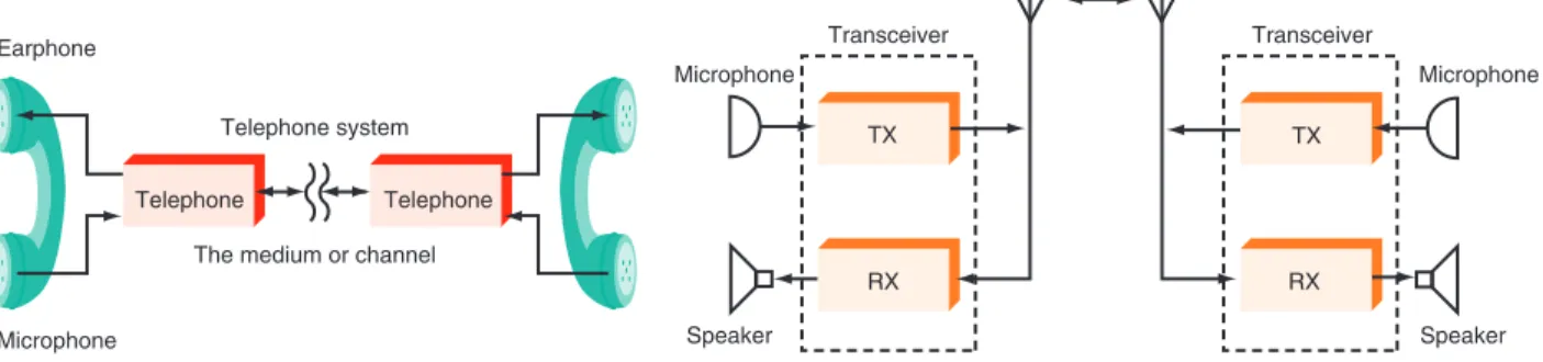
1-2 Communication Systems
GOOD TO KNOW
Transmitter
Communication Channel
The earth can be used as a communication medium because it conducts electricity and can transmit low-frequency sound waves. AC power lines, the electrical conductors that carry the power to operate almost all of our electrical and electronic devices, can also be used as communication channels.
Receivers
The signals to be transmitted are simply superimposed or added to the mains voltage. It is used for some types of remote control of electrical equipment and in some LANs.
Transceivers
Although the most commonly used media are conductive cables and free space (radio), other types of media are used in special communication systems. Active sonar uses an echo-reflective technique similar to that used in radar to determine how far away underwater objects are and in what direction they are moving.
Attenuation
Noise
1-3 Types of Electronic Communication
Simplex
Full Duplex
Half Duplex
Analog Signals
Digital Signals
If digital data is converted to analog signals, such as tones in the audio frequency range, they can be transmitted over the telephone network. The data can then be efficiently transmitted in digital form and processed by computers and other digital circuits.
1-4 Modulation and Multiplexing
Many transmissions are signals that originate in digital form, such as telegraphic messages or computer data, but must be converted to analog form to match the transmission medium. An example is the transmission of digital data over a telephone network that was designed only to process analog voice signals.
Baseband Transmission
In a communication system, baseband information signals may be transmitted directly and unchanged over the medium or may be used to modulate a carrier wave for transmission over the medium. Putting the original voice, video or digital signals directly into the medium is called baseband transmission.
Broadband Transmission
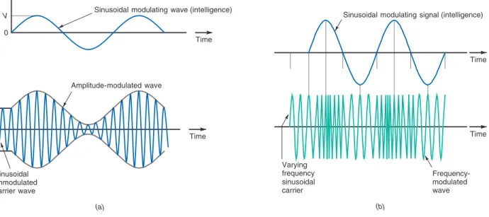
Higher frequency carriers radiate into space more efficiently than baseband signals themselves. In AM, the baseband information signal called the modulating signal changes the amplitude of the higher frequency carrier signal, as shown in Fig.
Multiplexing
1-5 The Electromagnetic Spectrum
Frequency and Wavelength
PIONEERS
Wavelength is the distance traveled by one wave cycle and is usually expressed in meters. If the signal is an electromagnetic wave, one wavelength is the distance one cycle travels in free space.
Frequencies in this range are also used as subcarriers, signals that are modulated by the baseband information. Some radar and navigation services occupy this part of the frequency spectrum, and amateur radio also have bands in this range.
The Optical Spectrum
1-6 Bandwidth
Channel Bandwidth
The term channel bandwidth refers to the range of frequencies required to transmit the desired information. As communication activities have grown over the years, there has been an ongoing demand for more frequency channels over which communication can be transmitted.
More Room at the Top
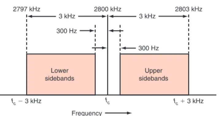
The bandwidth of the AM signal described above is the difference between the highest and lowest transmission frequencies: BW51005 kHz2995 kHz510 kHz. Many of the techniques discussed later in this book were developed in an attempt to minimize transmission bandwidth.
Spectrum Management
Standards
European Telecommunications Standards Institute (ETSI)—www.etsi.org Institute of Electrical and Electronics Engineers (IEEE)—www.ieee.org International Telecommunication Union (ITU)—www.itu.org. Internet Engineering Task Force (IETF)—www.ietf.org Optical Internetworking Forum (IF)—www.oiforum.com.
1-7 A Survey of Communication Applications
Individuals can become licensed "hams" to build and operate two-way radio equipment for personal communication with other radio amateurs. Citizens band (CB) radio is a special service that any individual can use to communicate personally with others.
1-8 Jobs and Careers in the Communication Industry
Types of Jobs
They may be involved in the actual construction and assembly of the equipment, but are more often involved in the final testing and measurements of the finished products. There are many jobs in the communications industry other than engineering and technician jobs.
Major Employers
The pay potential in sales is generally much higher than in the engineering or service positions. Most of the jobs available in the resale segment of the industry are in sales, service and training.
Licensing and Certifi cation
CHAPTER REVIEW
Online Activity
1-1 Exploring the Regulatory Agencies
1-2 Examining FCC Rules and Regulations
1-3 Investigate Licensing and Certifi cation
Questions
Name three other types of jobs in the field of electronic communications that do not involve engineering or technician work. Assume that you have a wireless application that you would like to design, build and sell as a commercial product.
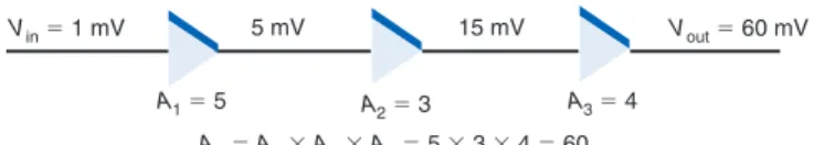
2-1 Gain, Attenuation, and Decibels
Gain
When multiple attenuation circuits are cascaded, the total attenuation is again the product of the individual attenuations. The overall gain or attenuation of a circuit is simply the product of the attenuation and gain factors.
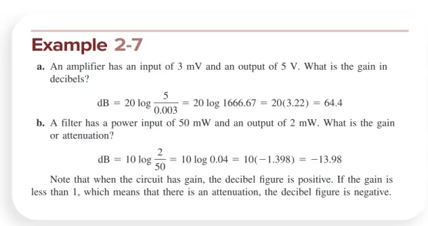
Decibels
Remember that the logarithm of y of a number N is the power to which the base 10 must be raised to get the number. Here, Pout is the output power or some power value you want to compare to 1 mW, and 0.001 is 1 mW expressed in watts.
2-2 Tuned Circuits
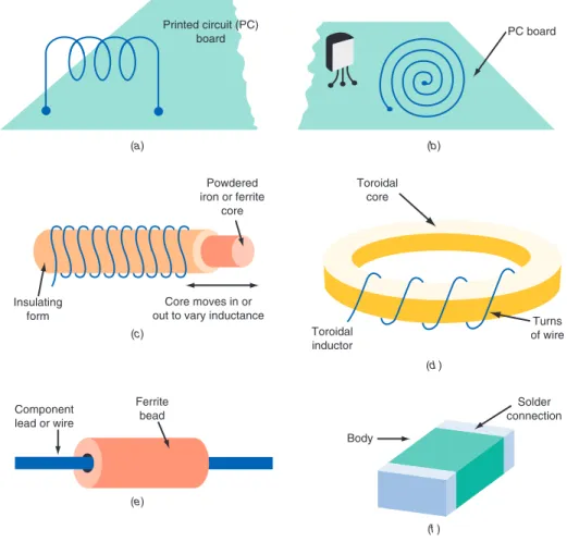
Reactive Components
In addition to the resistance of the wire in an inductor, there is coil capacitance between the turns of the coil. This is the ratio of the power returned to the circuit to the power actually delivered by the resistance of the coil.
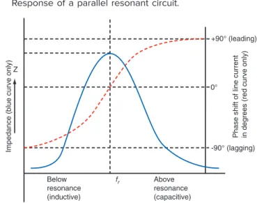
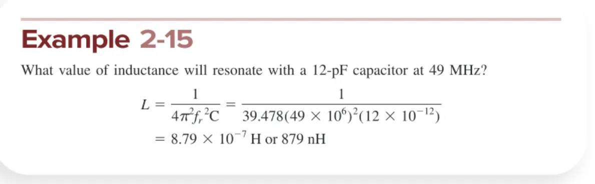
Tuned Circuits and Resonance
Recall that the Q of an inductor is the ratio of the inductive reactance to the resistance of the circuit. The total impedance of the circuit at resonance is equal to the equivalent parallel resistance:.
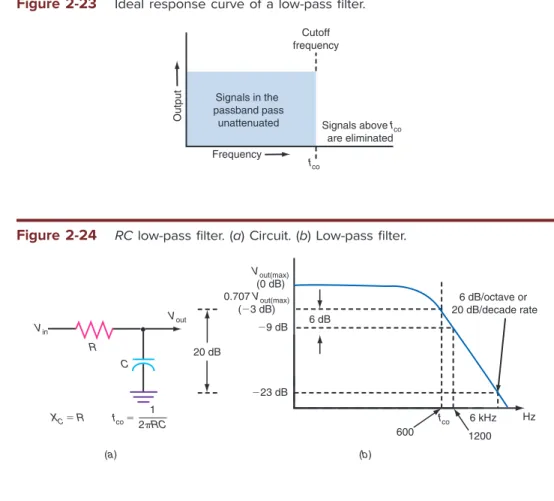
2-3 Filters
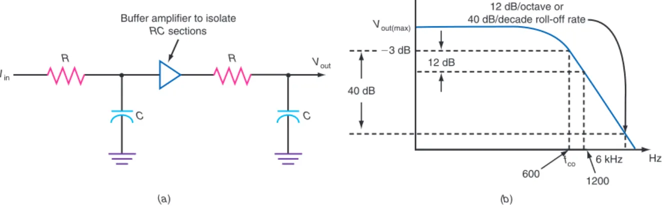
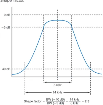
RC Filters
If the cutoff frequency of each RC section is the same, the total cutoff frequency for the entire filter will be slightly lower. The response curve for this RL i lter is the same as that shown in Fig.
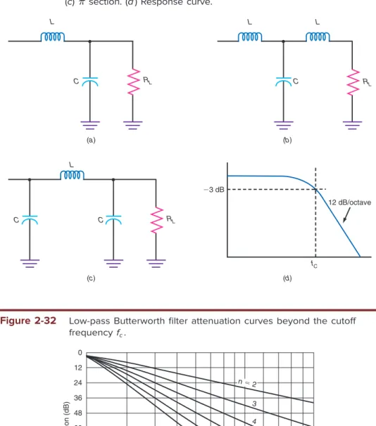
LC Filters
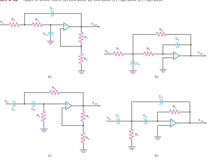
For LC low-pass and high-pass filters, the number of poles is equal to the number of reactive components in the filter. The faster the convolution or the higher the degree of attenuation, the more selective the filter, i.e. it can better distinguish between two closely spaced signals, one desirable and the other undesirable.
Types of Filters
At frequencies above and below the center resonant frequency, the impedance of the parallel tuned circuit is low compared to that of the resistor. At frequencies above and below the center rejection or notch frequency, the LC path impedance is high compared to the resistance.

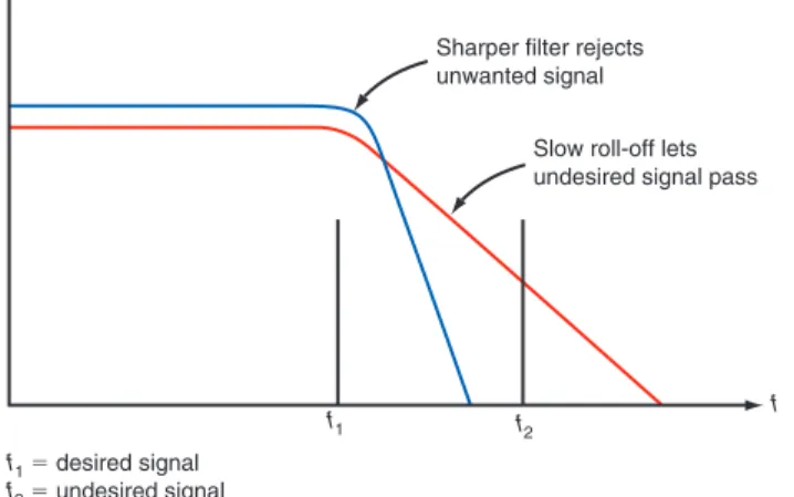
Active Filters
Active i lters are made with integrated circuit (IC) op amps and discrete RC networks. The primary disadvantage of active filters is that their upper operating frequency is limited by the frequency response of the op-amps and the practical sizes of resistors and capacitors.
Crystal and Ceramic Filters
If the frequency of the signal applied to the crystal is higher than fS, the crystal appears inductive. At this parallel resonant frequency fP, the impedance of the circuit is resistive but extremely high.
Switched Capacitor Filters
The higher the clock frequency compared to the frequency of the input signal, the smaller this effect. A sample of the input voltage is stored as a charge on each capacitor when it is connected to the input.
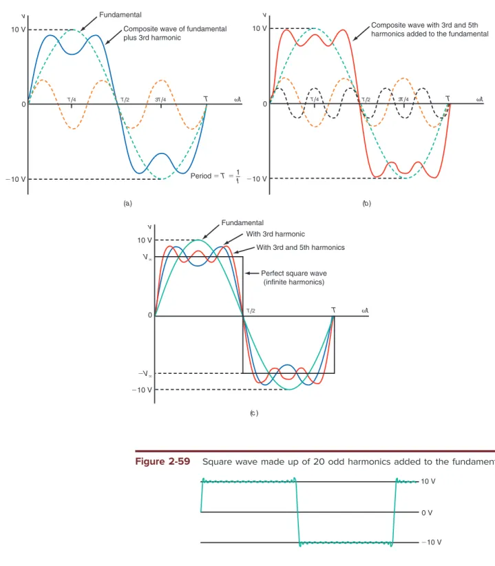
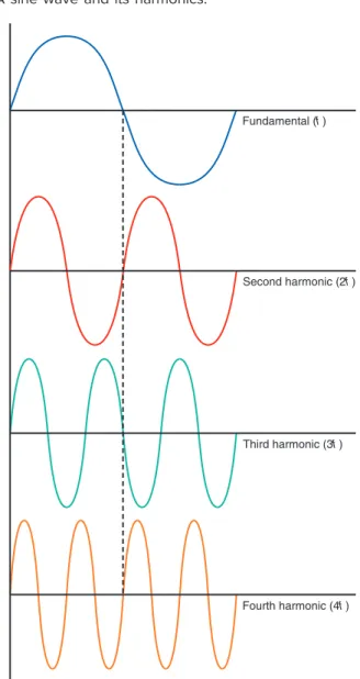
2-4 Fourier Theory
One of the methods used to do this is Fourier analysis, which provides a means to accurately analyze the content of more complex non-sinusoidal signals.
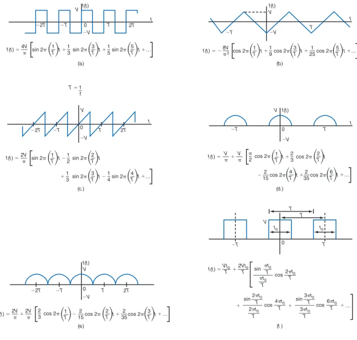
Basic Concepts
If the square wave is direct current instead of alternating current, Figure 2-60(f) shows the Fourier expression for a direct current square wave where the average direct current component is Vt0/T.
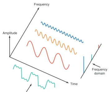
Time Domain Versus Frequency Domain
Find (a) the frequency of the fth harmonic and (b) the rms value of the fth harmonic. Frequency domain plots for some of the other common nonsinusoidal waves are also shown in Figs.
The Importance of Fourier Theory
Signals and waveforms in communications applications are expressed using both time-domain and frequency-domain plots, but in many cases the frequency-domain plot is far more useful. Like the oscilloscope, the spectrum analyzer uses a cathode ray tube for display, but the horizontal sweep axis is calibrated in hertz and the vertical axis is calibrated in volts or power units or decibels.
Pulse Spectrum
The horizontal axis is frequency plotted in steps of the pulse repetition frequency f , where f51/T and T is the period. The first component is the average DC component at zero frequency Vt0/T, where V is the peak voltage value of the pulse.

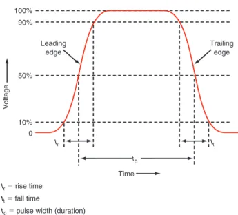
The Relationship Between Rise Time and Bandwidth
What this means is that the vertical amplifier of the oscilloscope has a bandwidth sufficient to pass a sufficient number of harmonics so that the resulting square wave has a rise time of 2 ns. Remember that the bandwidth or upper limit frequency derived from the rise time formula on the previous page only passes the harmonics necessary to support the rise time.
2-1 Exploring Filter Options
What is the bandwidth of a parallel resonant circuit that has an inductance of 33 µH with a resistance of 14 V and a capacitance of 48 pF. A parallel resonant circuit has an inductance of 800 nH, a winding resistance of 3 V, and a capacitance of 15 pF.
Amplitude Modulation Fundamentals
3-1 AM Concepts
3-1, the modulating signal uses the peak value of the carrier instead of zero as its reference point. In general, the amplitude of the modulating signal should be less than the amplitude of the carrier wave.
3-2 Modulation Index and Percentage of Modulation
A circuit must be able to produce mathematical multiplication of the carrier and modulating signals in order for AM to occur. Its two inputs, the carrier and modulating signal, and the resulting outputs are shown in Fig.
Overmodulation and Distortion
If the amplitude of the modulated signal is less than the amplitude of the carrier, no distortion will occur. Typically, the amplitude of the modulated signal is adjusted so that only the vocal peaks result in 100% modulation.
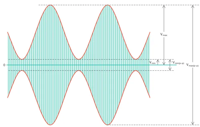
Percentage of Modulation
Vmax is half the peak value at the top of the AM signal, or Vmax (p 2p)/2. At this time, Vmin50 and Vmax52Vm, where Vm is the peak value of the modulating signal.
3-3 Sidebands and the Frequency Domain
Sideband Calculations
If you observe an AM signal on an oscilloscope, you can see the amplitude variations of the carrier with respect to time. An AM signal is actually a composite signal formed from several components: the carrier sine wave is added to the upper and lower sidebands, as the equation indicates.
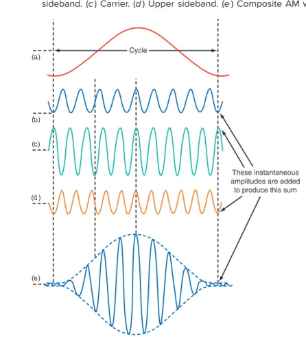
Frequency-Domain Representation of AM
The total bandwidth of an AM signal is calculated by calculating the maximum and minimum sideband frequencies. In the case of a speech signal whose maximum frequency is 3 kHz, the total bandwidth is simply.
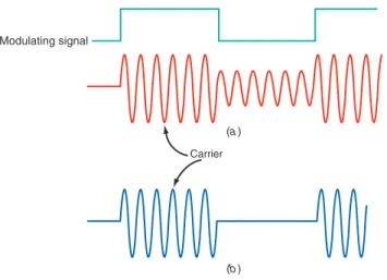
Pulse Modulation
3-13 shows the transfer of the letter P, which is dot-dash-dash-dot (pronounced “dit-dah-dah-dit”). The sidebands are the result of the frequency or repetition rate of the pulses themselves plus their harmonics.
3-4 AM Power
For a 100 percent modulated AM transmitter, the total sideband power is always half the carrier power. The total power for the AM signal is the sum of the carrier and sideband power, or 75 kW.
3-5 Single-Sideband Modulation
Despite its inefficiency, AM is still widely used because it is simple and effective. It is used in AM radio broadcasts, CB radio, TV broadcasts and aircraft tower communications.
DSB Signals
A unique characteristic of the DSB signal is the phase transitions that occur at the lower amplitude parts of the wave. Although eliminating the carrier in DSB AM saves considerable power, DSB is not widely used because the signal is difficult to demodulate (recover) at the receiver.
SSB Signals
The primary benei t of an SSB signal is that the spectrum space it occupies is only one-half that of AM and DSB signals. This greatly conserves spectrum space and
As shown, the spectral space occupied by a DSB signal is the same as that of a conventional AM signal. However, since there is no carrier transmission in an SSB system, no signals are present when the information signal is zero.
Disadvantages of DSB and SSB
3-17 shows the frequency and time domain representations of an SSB signal produced when a stable 2 kHz sine wave tone modulates a 14.3 MHz carrier. To solve this problem, sometimes a low level carrier signal is transmitted along with the two sidebands in DSB or a single sideband in SSB.
Signal Power Considerations
Because the carrier has a low power level, the essential benefits of SSB are retained, but a weak carrier is received so that it can be amplified and reinserted to recover the original information.
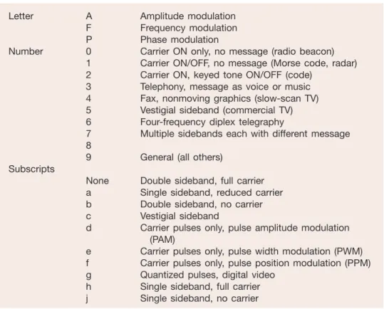
3-6 Classifi cation of Radio Emissions
Note that there are special designations for facsimile and pulse transmissions and that #9 covers any special modulations or techniques not covered elsewhere. The designation 20A3h refers to an AM SSB signal with a full carrier and a message frequency of up to 20 kHz.
3-1 AM and SSB Radio Applications
What is the name of the type of signal that appears on an oscilloscope. What is the name of an AM signal whose carrier wave is modulated by binary pulses.
Amplitude Modulator and Demodulator Circuits
4-1 Basic Principles of Amplitude Modulation
AM in the Time Domain
AM in the Frequency Domain
The fourth term, the product of the carrier and modulating signal sine waves, is the AM wave. The third term cos 2ωc t is a sine wave at twice the frequency of the carrier, i.e. the second harmonic of the carrier.
4-2 Amplitude Modulators
Low-Level AM
The output is a function of the difference between inputs V1 and V2; that is, Vout5A(V22V1), where A is the circuit gain. The gain of a differential amplifier is a function of the emitter current and the value of the collector resistors.
High-Level AM
The secondary winding of the modulating transformer is connected in series with the collector supply voltage VCC of the class C amplifier. For 100 percent modulation, the peak of the modulating signal across the secondary of T1 must equal the supply voltage.

4-3 Amplitude Demodulators
The emitter-follower modulator must dissipate as much current as the class C RF amplifier. This means that the rest of the supply voltage, or another 12 V, appears between the emitter and the collector of Q2.
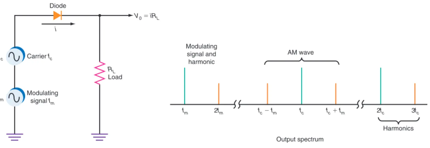
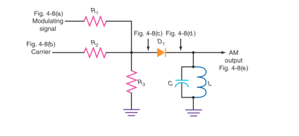
Diode Detectors
Distortion of the original signal can occur if the time constant of the load resistor R1. Another way to view the performance of a diode detector is in the frequency domain.
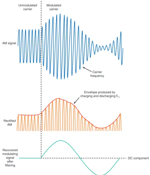
Crystal Radio Receivers
The components of the AM signal are the carrier wave fc, the upper sideband fc1fm and the lower sideband fc2fm. Since the carrier frequency is much higher than that of the modulating signal, the carrier signal can be easily filtered out with a simple low-pass filter.
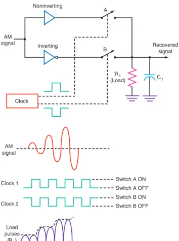
Synchronous Detection
The AM signal to be demodulated is applied to a highly selective bandpass filter that selects the carrier and suppresses sidebands, thereby removing most amplitude variations. This signal is amplified and applied to a clipper or limiter that removes any residual amplitude variation from the signal, leaving only the carrier.
4-4 Balanced Modulators
During this time the negative cycles of the AM signal occur, causing the lower output of the secondary winding to become positive. When D2 conducts, the positive half cycles are passed to the load, and the circuit performs full wave rectification.
Lattice Modulators
Again, a portion of the modulating signal at the secondary of T1 is applied to the primary of T2, but this time the leads are effectively reversed due to the connections of D3 and D4. Note that the envelope of the output signal is not the shape of the modulating signal.
IC Balanced Modulators
The result of switching the carrier on and off and varying the modulating signal as shown produces the classic DSB output signal described earlier [see Fig. The input impedances of the carrier and modulating signal are equal to the input impedance values.

4-5 SSB Circuits
Generating SSB Signals: The Filter Method
However, the choice of upper or lower sideband as the standard varies from service to service, so it is important to know which one has been used to receive the SSB signal correctly. What should be the approximate center frequency of the bandpass filter to select the lower sideband.

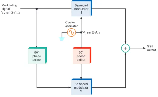
Generating SSB Signals: Phasing
One of the circuits commonly used to produce a 90° phase shift over a wide bandwidth is shown in Fig. 4-32 shown and the 90° phase-shifted signal to balanced modulator 1 will cause the upper sideband to be selected instead of the lower sideband.
DSB and SSB Demodulation
The phase relationship of the carrier can also be changed for this change. The design of phase-type SSB generators is critical if complete rejection of the unwanted sideband is to be achieved.
4-1 ASK Transmitters and Receivers
All that needs to be done is to connect a low pass filter to the output to get rid of the unwanted high frequency signal while sending the desired differential signal. An SSB generator has a 9-MHz carrier and is used to transmit voice frequencies in the 300- to 3300-Hz range.
Fundamentals of
Frequency Modulation
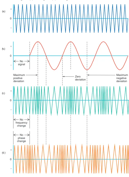
5-1 Basic Principles of Frequency Modulation
For example, when the modulating signal is a binary 0, the carrier frequency is the center frequency value. When the modulating signal is a binary 1, the carrier frequency changes abruptly to a higher frequency level.
5-2 Principles of Phase Modulation
In PM, the amount of carrier deviation is proportional to the rate of change of the modulating signal, i.e., the derivative of the calculation. With a sine wave modulating signal, the PM carrier appears to be frequency modulated by the cosine of the modulating signal.
Relationship Between the Modulating Signal and Carrier Deviation
However, higher modulating frequencies produce a faster rate of change of the modulating voltage and thus greater frequency deviation. In FM, frequency deviation is only proportional to the amplitude of the modulating signal, regardless of its frequency.
Converting PM to FM
The higher the modulating signal frequency, the shorter its period and the faster the voltage changes. Although the higher modulating frequencies give a greater rate of change and thus a greater frequency deviation, this is offset by the lower amplitude of the modulating signal, which gives less phase shift and thus less frequency deviation.
Phase-Shift Keying
5-3 Modulation Index and Sidebands
Since the FM signal is the sum of the sideband frequencies, the sideband amplitudes must vary with frequency deviation and modulation frequency if their sum is to produce an FM signal of constant amplitude but variable frequency. However, the bandwidth of an FM signal is usually much wider than that of an AM signal with the same modulating signal.
Modulation Index
The number of sidebands produced, their amplitude and spacing depends on the frequency deviation and the modulating frequency. In most communication systems using FM, maximum limits are placed on both the frequency deviation and the modulating frequency.
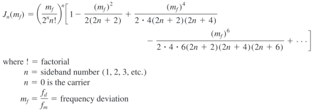
Bessel Functions
The amplitudes of the sidebands are determined by the Jn coefficients, which in turn are determined by the value of the modulation index. The carrier and sideband amplitudes and polarities are plotted on the vertical axis; the modulation index is plotted on the horizontal axis.
FM Signal Bandwidth
For example, if the modulating signal is a square wave, the fundamental sine wave and all odd harmonics modulate the carrier wave. What is the maximum bandwidth of an FM signal with a deviation of 30 kHz and a maximum modulating signal of 5 kHz, as determined by (a) Fig.
This does not affect the information content of the FM signal, as it is contained solely in the frequency variations of the carrier wave. Even if the peaks of the FM signal itself are clipped or monitored and the resulting signal is distorted, no information is lost.
Noise and Phase Shift
The total effect of the shift depends on the maximum allowed frequency shift for the application. The ratio of the shift produced by the noise to the maximum allowable deviation is.
Preemphasis
The pre-emphasis circuit increases the energy content of higher frequency signals so that they become stronger than the high frequency noise components. The combined effect of pre-emphasis and emphasis is to increase the signal-to-noise ratio for high-frequency components during transmission so that they are louder and not masked by noise.
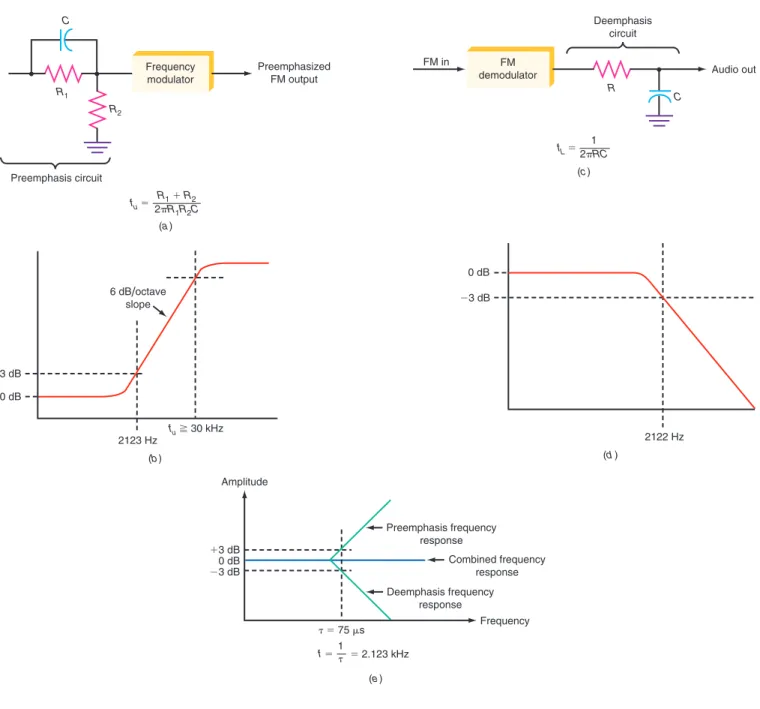
To return the frequency response to its normal, "at" level, a demphasis circuit, a simple low-pass i lter with a time constant of 75 µs, is used at the receiver [see Fig. Signals above its cutoff frequency of 2123 Hz are attenuated at a rate of 6 dB per second. octave.
Advantages of FM
The AM signal is generated at a lower level and then amplified by linear amplifiers to produce the final RF signal. In fact, FM signals are always generated at a lower level and then amplified by a series of Class C amplifiers to increase their power.
Disadvantages of FM
Linear amplifiers are Class A or Class B and are much less efficient than Class C amplifiers. FM signals have a constant amplitude and therefore there is no need to use linear amplifiers to increase their power level.
FM and AM Applications
5-1 FM Radio Applications
What is the name of the mathematical equation used to solve for the number and amplitude of sidebands in an FM signal. What is the nature of the modulating signals most negatively affected by noise on an FM signal.
FM Circuits
6-1 Frequency Modulators
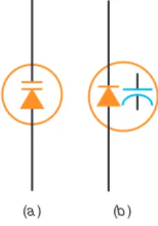
Varactor Operation
The width of the depletion layer determines the width of the dielectric and therefore the amount of capacitance. Reducing the amount of reverse bias narrows the depletion region; the plates of the capacitor are actually closer together, creating a higher capacitance.
Varactor Modulators
Even with high-quality components and optimal design, the frequency of LC oscillators will vary due to temperature changes, circuit voltage variations, and other factors. The LC oscillators are simply not stable enough to meet the stringent requirements set by the FCC.
Frequency-Modulating a Crystal Oscillator
Although it is possible to achieve a deviation of only a few hundred cycles from the crystal oscillator frequency, the total deviation can be increased by using frequency multiplication circuits after the carrier oscillator. The carrier is generated by a 6.5 MHz crystal oscillator, followed by frequency multiplication circuits that increase the frequency by a factor of 24 (6.5 MHz3245156 MHz).
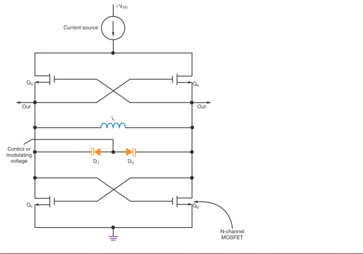
Voltage-Controlled Oscillators
A frequency multiplier is one whose output frequency is some integer multiple of the input frequency. When this deviation is multiplied by a factor of 24 in the frequency multiplier circuits, it increases to Hz or 4.8 kHz, which is close to the desired deviation.
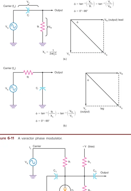
6-2 Phase Modulators
Since this is PM, the actual deviation is also proportional to the frequency of the modulated signal. In this arrangement, there is an inverse relationship between the polarity of the modulated signal and the direction of the frequency deviation.
6-3 Frequency Demodulators
Slope Detectors
The slope detector is never used in practice, but it does demonstrate the principle of FM demodulation, that is, the conversion of a frequency variation to a voltage variation. These include the Foster-Seeley discriminator and the ratio detector, neither of which are used in modern equipment.
Pulse-Averaging Discriminators
When a single-shot pulse occurs, the capacitor in the lter is charged to the amplitude of the pulse. When the time interval between pulses is long, however, the capacitor loses some of its charge to the load, so the average dc output is low.
Quadrature Detectors