Selected examples show a Multisim® or LT Spice exercise linked to a file on the companion website that contains the circuit shown in the example. Device Usage: Complete PA system. A class AB power amplifier follows the audio preamplifier and drives the loudspeaker, as shown in the PA system block diagram in Figure 7–33.
Global Edition Acknowledgments
B riEf c ontEnts
I ntroductIon to
S emIconductorS
The Bohr Model
Atomic Number
The atomic numbers of all elements are shown in the periodic table of elements in Figure 1–3.
Electrons and Shells
Maximum number of electrons in each shell The maximum number of electrons (Ne) that can exist in each shell of an atom is a fact of nature and can be calculated with the formula,.

Valence Electrons
Ionization
The Quantum Model
Each atom can be described by an electron configuration table that shows the shells or energy levels, the orbitals, and the number of electrons in each orbital. Three-dimensional quantum model of the sodium atom, showing the orbitals and the number of electrons in each orbital.
1–2 m AterIAlS u Sed In e lectronIc d evIceS
In a three-dimensional representation of the quantum model of an atom, the s-orbitals are shaped like spheres with the nucleus in the center. For example, a representation of the quantum model of a sodium atom (Na) with eleven electrons, as shown in Figure 1–5.
Insulators, Conductors, and Semiconductors
Band Gap
Comparison of a Semiconductor Atom to a Conductor Atom
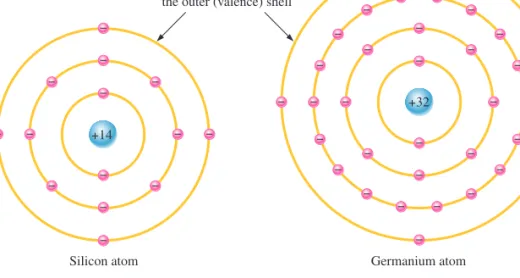
Silicon and Germanium
The valence electrons in germanium are in the fourth shell, while the electrons in silicon are in the third shell, closer to the nucleus. With its four valence electrons, a silicon (Si) atom shares an electron with each of its four neighbors.
Conduction Electrons and Holes
Electron and Hole Current
Type Semiconductor
Type Semiconductor
Although the majority of current carriers in p-type material are holes, there are also some conduction-band electrons that are created when electron-hole pairs are thermally generated. These conduction band electrons are not produced by the addition of the trivalent impurity atoms.
The blue arrows between the positive and negative charges in the depletion region represent the electric field. In the depletion region there are many positive charges and many negative charges on either side of the p-n junction.
Energy Diagrams of the PN Junction and Depletion Region
This means that external energy must be applied to move the electrons across the electric field barrier in the depletion region. The electric field potential difference in the depletion region is the amount of voltage required to move electrons through the electric field.
SUMMARY
When an electron breaks away to become free, it leaves a hole in the valence band called an electron-hole pair. Electron-hole pairs are continuously generated thermally so that there are always free electrons in the material.
KEY FORMULA
In a semiconductor crystal, the atoms are held together by. a) the interaction of valence electrons (b) attractive forces (c) covalent bonds (d) answers (a), (b) and (c). Holes in an n-type semiconductor are. a) minority carriers produced thermally (b) minority carriers produced by doping (c) majority carriers produced thermally (d) majority carriers produced by doping Section 1–5 23.
D ioDes anD a pplications
The Diode
The bias voltage source provides sufficient energy to the free electrons so that they overcome the barrier potential of the depletion region and pass into the p region. A forward biased diode showing majority carrier flow and the voltage due to the blocking potential across the depletion region.
Reverse Bias
I Characteristic for Forward Bias
As you gradually increase the forward bias voltage, the forward current and the voltage across the diode gradually increase, as shown in Figure 2–9(a). Point B corresponds to Figure 2–10(a) where the forward voltage is less than the barrier potential of 0.7 V.
I Characteristic for Reverse Bias
Unlike a linear resistor, the resistance of a forward-biased diode is not constant over the entire curve. Below the knee of the curve, the resistance is greatest because the current increases very little for a given change in voltage (r9d =DVF>DIF).
The Complete V-I Characteristic Curve
The internal resistance of electronic devices is usually indicated by the lowercase italicized letters r with a prime number instead of the standard R. The resistance begins to decrease in the region of the knee of the curve and becomes the smallest above the knee, where there is a large change in current for a given change in voltage.
Bias Connections
Diode Approximations
Since the barrier potential and the forward dynamic resistance are neglected, the diode is assumed to have zero voltage across it when it is forward biased, as indicated by the portion of the curve that is on the positive vertical axis. The diode is assumed to have zero reverse current, as indicated by the portion of the curve that is on the negative horizontal axis.
Measure the voltages across the diode and the resistance in both circuits and compare with the calculated results in this example.
The Basic DC Power Supply
Half-Wave Rectifier Operation
Related Problem Determine the average value of the half-wave voltage if its peak amplitude is 12 V.
Effect of the Barrier Potential on the Half-Wave Rectifier Output
Plot the output voltages of each rectifier for the indicated input voltages, as shown in Figure 2–24. Related Problem Determine the peak output voltages for the rectifiers in Figure 2–24 if the peak input in part (a) is 3 V and the peak input in part (b) is 50 V.
Peak Inverse Voltage (PIV)
Note that the barrier potential could have been neglected in circuit (b) with very little error (0.7%); but if it is neglected in circuit (a), a significant error results (14%). Open the Multisim file EXM02-03 or the LT Spice file EXS02-03 in the Examples folder on the website.
Transformer Coupling
Determine the maximum value of the output voltage for Figure 2–28 if the turns ratio is 0.5. What is the maximum value of the output voltage of a half-wave rectifier with a maximum input sinusoidal voltage of 25 V.
The number of positive changes that make up the half-wave rectified voltage is twice that of the half-wave voltage for the same time interval. Related Problem Find the average value of a half-wave rectified voltage if its peak is 155 V.
Center-Tapped Full-Wave Rectifier Operation
In this case, the total secondary voltage (Vsec) is twice the primary voltage (2Vpri), so the voltage across each half of the secondary is equal to Vpri. In any case, the output voltage of a center-tapped full-wave rectifier is always half the total secondary voltage minus the diode drop, regardless of the turns ratio.
Bridge Full-Wave Rectifier Operation
For the ideal diode model (forward-biased diodes D1 and D2 shown in green), PIV = Vp(out). Related Problem Determine the maximum output voltage for the bridge rectifier in Figure 2–41 if the transformer produces an rms secondary voltage of 30 V.
2–6 p oWer s upply f ilters anD r egulators
Which type of full wave rectifier has higher output voltage for the same input voltage and transformer turns ratio. Define voltage ripple ◆ Calculate the ripple factor ◆ Calculate the output voltage of a filtered full-wave rectifier ◆ Discuss inrush current.
Capacitor-Input Filter
V = 0.039 The percent ripple is 3.9%
Surge Current in the Capacitor Input Filter Before the switch in Figure 2–49 closes, the filter capacitor is uncharged. In direct current supplies, a fuse is always placed in the primary circuit of the transformer, as shown in Figure 2–49.
Voltage Regulators
The worst situation occurs when the switch is closed at the peak of the secondary voltage and the maximum inrush current Isurge(max) occurs as shown in the figure. The fuse rating is determined by calculating the power in the supplied load, which is the output power.
Percent Regulation
Diode Limiters
A positively biased limiter is shown in Figure 2–60(a), a negatively biased limiter is shown in part (b), and a variable positive bias circuit using a potentiometer voltage divider is shown in part (c). Related Problem How would you change the voltage divider in Figure 2–61 to limit the output voltage to +6.7 V.
Diode Clampers
What is the output voltage you would expect across RL in the clamp circuit of Fig. 2-65. Related Problem What is the output voltage that would be observed across RL in Figure 2–65 for C=22 mF and RL=18 kV.
2–8 V oltage m ultipliers
Voltage Doubler
When the secondary voltage is positive, D1 is forward biased and C1 charges to approx. Vp, as shown in part (a). During the negative half cycle, D2 is forward biased and C2 charges to approx. Vp, as shown in part (b).
Voltage Tripler
Voltage Quadrupler
The mechanical information, such as package dimensions, is not shown on this particular data sheet, but is generally available from the manufacturer. Note on this data sheet that there are three categories of data given in tabular form and four types of characteristics shown in graphical form.
Data Categories
PD Average power dissipation is the amount of power the diode can dissipate under any condition. Above 758C, the diode cannot handle 1 A, so the maximum current must be reduced as indicated by the curve.
Testing a Diode
Troubleshooting a Power Supply
At this point you have isolated the problem to the part of the circuit between the last test point and the current test point where the voltage is correct. If the measurement in the middle of the circuit shows no voltage or an incorrect voltage, you know the fault is between the input and that test point.
Fault Analysis
Another fault that will cause the same symptom is an open in the transformer's secondary winding. If only one of the diodes in the rectifier is open, there should be a half-wave rectified output voltage, so that's not the problem.
Multisim Troubleshooting Exercises
Because the rectifier in a single IC package exceeds the specifications and requires less wiring on the board, takes up less space, and requires only one component to store and handle compared to four, it is the best choice. The power switch shown in the original schematic will be on the PC board case and is not shown for the test setup.
SUMMARY OF DIODE BIAS
SUMMARY OF POWER SUPPLY RECTIFIERS
Section 2–2 ◆ The V-I characteristic curve shows the diode current as a function of voltage across the diode. Section 2–3 ◆ The ideal model represents the diode as a closed switch in forward bias and as an open switch in reverse bias.
KEY FORMULAS
If the frequency of the input voltage in Figure 2–36 is increased, the output voltage will (a) increase (b) decrease (c) not change. If the input voltage in Figure 2–65 is increased, the peak negative value of the output voltage will (a) increase (b) decrease (c) not change.
3 S pecial -p urpoSe D ioDeS
Zener Breakdown
Zener diodes with breakdown voltages of less than about 5 V operate predominantly at Zener breakdown. Zeners are commercially available with breakdown voltages from less than 1 V to more than 250 V with specified tolerances of 1% to 20%.
Breakdown Characteristics
Near the Zener breakdown voltage (VZ), the field is intense enough to pull electrons from their valence bands and create current.
Zener Equivalent Circuits
It is best to avoid placing a zener diode near the knee of the curve because the impedance changes dramatically in that area. When a Zener diode is operating normally, it will be in reverse breakdown and you must observe the rated breakdown voltage across it.
Temperature Coefficient
Zener Power Dissipation and Derating
Zener Diode Datasheet Information
Zener voltage (VZ) . The zener voltage is measured with the device terminal in thermal equilibrium at the lead temperature TL) at 308C ± 18C and 3/8" lead length. The change in voltage due to the increase in current above the IZ value causes the zener terminal voltage to increase.
The change in voltage due to the decrease in current below the test current causes the zener terminal voltage to decrease.
Zener Regulation with a Variable Input Voltage
As the input voltage varies (within limits), the zener diode maintains an almost constant output voltage across its terminals. Determine the minimum and maximum input voltages that can be regulated by the zener diode in Figure 3–11.
Zener Regulation with a Variable Load
From No Load to Full Load
For the minimum load resistance (maximum load current), the zener current is minimum (IZK =0.25 mA) as shown in Figure 3–16(b). Related Problem Repeat each part of the preceding analysis if the zener is changed to a 1N4742A 12 V device.
Zener Limiter
In a zener diode regulator, what value of load resistance results in the maximum zener current. The p and n regions are conductive and act as the capacitor plates, as illustrated in Figure 3–21.
A varactor is a diode that always operates in reverse bias and is doped to maximize the inherent capacitance of the depletion region.
Basic Operation
Varactor Capacitance Ratio
To avoid harmonic distortion, you will often see two varactor diodes back to back, as shown in Figure 3–25(a) with the reverse DC voltage applied to both devices simultaneously. The Zetex 832A varactor diode is available in a back-to-back configuration in a SOT23 surface mount package or as a single diode in a SOD523 surface mount package, as shown in Figure 3–25(b).
An Application
Back-to-back configuration One of the disadvantages of using only a single varactor diode in certain applications, such as RF tuning, is that if the diode is biased in the direction of the RF signal during part of the AC cycle, its reverse leakage will increase instantly. A resonant bandpass filter that uses a varactor diode to adjust the resonant frequency over a specified range. a) Given that the capacitance of a certain varactor is approximately 40 pF at a bias of 0 V and that the capacitance at a bias of 2 V is 22 pF, determine the capacitance at a reverse bias of 20 V using a minimum capacitance ratio of 5.0. b) Using the capacitance at 0 V and 20 V biases, calculate the resonant frequencies at the extreme biases for the circuit in Fig. 3–26 if L =2 mH. c) The Multsim circuit simulation is shown in Figure 3-27.
The Light-Emitting Diode (LED)
The amount of energy converted to light is directly proportional to the forward current, as shown in Figure 3–30(b). Light Emission An LED emits light over a specific wavelength range, as indicated by the output spectral curves in Figure 3–31.
LED Datasheet Information
Applications
High-Intensity LEDs
The particular configuration of the LED circuit depends on the voltage and color of the LED. The voltage drop across the series limiting resistor is V =12 V-7.5 V=4.5 V The value of the limiting resistor is.
The Organic LED (OLED)
Electrons are supplied to the emissive layer and removed from the conductive layer when there is current between the cathode and anode. Electrons from the emitting layer recombine with holes from the conducting layer near the junction of the two layers.
Quantum Dots
OLEDs can be sprayed onto special substrates, just as ink is sprayed onto paper during printing. They are superior in efficiency and power consumption to standard LEDs and can be recycled at the end of their life.
The Photodiode
An increase in the amount of light intensity, expressed as irradiance (mW/cm2), produces an increase in the reverse current, as shown by the graph in Figure 3–44(a). From the graph in Figure 3–44(b), you can see that the reverse current for this particular device is about 1.4 mA at a reverse-bias voltage of 10 V with an irradiance of 0.5 mW/cm2.
A grid of very thin conductive contact strips is deposited on top of the wafer by methods such as photoresist or silk screen, as shown in Figure 3–47(b). The thickness of the solar cell compared to the surface is greatly exaggerated for illustration purposes.
Solar Cell Characteristics
Solar Cell Panels
Manufacturers usually specify the output of a solar panel in terms of power at a certain solar radiation called the peak solar radiation which is 1000 W/m2. A typical solar panel with a nominal 12 V output can deliver 17 V at 3.5 A to a load under peak conditions.
The Laser Diode
The length of the pn junction is precisely related to the wavelength of the emitted light. Eventually, some photons randomly floating in the depletion region strike the reflected surfaces perpendicularly.
The Schottky Diode
In the case of a DVD player, a shorter wavelength is used and the recordings are denser, so they contain more data and the data is sampled faster. As with a CD player, the dimples and flats represent data, but in this case they are closer together and smaller to squeeze more data into the same amount of space.
The PIN Diode
Schottky is a fast switching diode and most of its applications make use of this feature. The LS family of TTL logic (LS stands for Low Power Schottky) is a type of digital integrated circuit that uses the Schottky diode.
The Step-Recovery Diode
There are no minority carriers and therefore no reverse leakage current as with other types of diodes. Since there are no minority carriers as in a conventional rectifier diode, there is a very fast response to a change in bias voltage.
The Tunnel Diode
If a tunnel diode is placed in series with the tank circuit and is biased at the center of the negative resistance portion of its characteristic curve, as shown in Figure 3-62, a sustained oscillation (constant sinusoidal voltage) will occur. exit. This is because the negative resistance characteristic of the tunnel diode opposes the positive resistance characteristic of the tank resistor.
Current Regulator Diode
The damping is due to the resistance of the tank, which prevents a stable oscillation because energy is lost when there is current through the resistor. In forward bias, diode regulation starts at the limiting voltage, VL, and extends up to POV (peak operating voltage).
A Zener-Regulated DC Power Supply
As shown in Figure 3-67, a no-load check that results in an output voltage greater than the maximum zener voltage but less than the power supply output voltage indicates that the zener has failed so that the impedance of his interior is larger than it should be. . If a zener regulator fails so that the zener impedance is greater than the specified value, is the output voltage more or less than it should be.
Device Application: Regulated DC Power Supply
A partial data sheet for a 7812 is shown in Figure 3–69(a) Note that there is a range of nominal output voltages, but it is typically 12 V. Fuse The fuse will be in series with the primary winding of the transformer, as shown in Figure 3–68.
SUMMARY OF DIODE SYMBOLS
If the amplitude of the input voltage in Figure 3–18(a) increases, the positive output voltage will (a) increase (b) decrease (c) not change. If the amplitude of the input voltage in Figure 3–19(a) is decreased, the amplitude of the output voltage will (a) increase (b) decrease (c) not change.
B ipolar J unction
Biasing
Operation
Most of the free electrons that have entered the base do not recombine with the holes because the base is very thin. The free electrons move through the collector region to the external circuit and then return to the emitter region along with the base current as shown.
Transistor Currents
Is the base region much thinner or much wider than the collector and emitter regions. If the collector current is 1 mA and the base current is 10 mA, what is the emitter current.
DC Beta (B DC ) and DC Alpha (A DC )
When the transistor is connected to DC biases as shown in Figure 4-6 for npn and pnp types, VBB biases the base-emitter junction and VCC reverse biases the base-collector junction. The base-bias voltage source, VBB, is the forward-biased base-emitter junction, and the collector-biased voltage source, VCC, is the reverse-biased base-collector junction.
Transistor DC Model
When the base-emitter junction is forward-biased, it is like a forward-biased diode and has a nominal forward voltage drop of.
BJT Circuit Analysis
The collector voltage with respect to emitter ground is VCE= VCC -VRC. Since the drop across RC is. the collector-to-emitter voltage can be written as VCE5 VCC2 ICRC.
Collector Characteristic Curves
This is indicated by the portion of the characteristic curve between points A and B in Figure 4–10(b). This is shown by the portion of the characteristic curve between points B and C in Figure 4–10(b).
Cutoff
Saturation
DC Load Line
Even at fixed IC and temperature values, bDC varies from device to device for a given type of transistor due to inconsistencies in the manufacturing process that cannot be avoided. The bDC determined at a given IC value is usually the minimum value, bDC(min), although sometimes maximum and typical values are also specified.
More About B DC
Maximum Transistor Ratings
VCC can be increased to 34.5 V, under the existing conditions, before VCE(max) is exceeded. If the base current is removed, causing the transistor to turn off, VCE(max) will be exceeded first because the entire supply voltage, VCC, will drop across the transistor.
Derating P D(max)
At present, however, it is not known whether PD(max) has been exceeded.
BJT Datasheet
These ratings are threshold values above which the usability of any semiconductor device may be degraded. Note that PD(max) is listed as PD under thermal characteristics, but on some datasheets it is listed under absolute maximum ratings.
DC and AC Quantities
The AC input voltage produces an AC base current, which results in a much larger AC collector current. This ac collector current produces an ac voltage across RC and thus produces an amplified, but inverted, representation of the ac input voltage in the active operating region, as illustrated in Figure 4–21.
Voltage Amplification
Since voltage gain is defined as the ratio of the output voltage to the input voltage, the ratio of Vc to Vb is the AC voltage gain, Av, of the transistor. What is the voltage gain of a transistor amplifier that has an output of 5 V rms and an input of 250 mV rms.
