The extension of the condition into the cladding can also be easily seen in the vertical cross-section. 225 3.9 FEM simulating a sudden cavity showing cross sections of the fields (through the center of the beam) and corresponding FFTs (λ/4 in substrate). 227 3.10 FEM simulations of our initial beam design showing cross sections of the fields. through the center of the beam) and corresponding FFTs (λ/4 in substrate).
233 3.12 FEM simulations of our extended beam design showing field cross sections. through the center of the beam) and the corresponding FFT (λ/4 in the substrate). 273 3.42 FEM simulations of our fixed-radius beam design showing field cross-sections. through the center of the beam) and the corresponding FFT (λ/4 in the substrate). All devices used 15 mirror periods (including the taper region) on each side of the cavity center.
Emitter characteristics
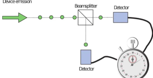
Here, the arrival of one photon from the pair can be used to signal the emission of the other, with the second detector only triggered when a photon is available. Despite the inefficiency of the pair creation process, these sources show improved brightness compared to atomic cascades. At zero delay, gp2qp0q gives a quantitative measure of the multiphoton emission probability.
Therefore, a minimum gp2qp0q is one of the most important metrics for any single photon source [45, 324]. To achieve strong anti-aggregation, some qualities of the system are immediately apparent. Beyond the actual generation of photons, achieving high efficiency means effectively collecting photons and channeling the emission in a well-defined spatial fashion.
Emitter types
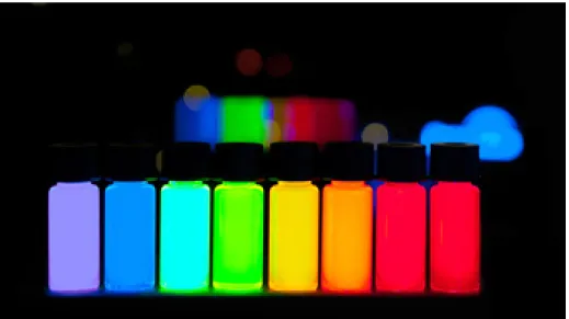
Broadly speaking, these fall into three categories: color centers, colloidal quantum dots (often called "semiconductor nanocrystals"), and self-assembled quantum dots (often "epitaxial quantum dots," "semiconductor quantum dots," or simply, "quantum dots"). The discrete spectra of colloidal quantum dots, also called 'artificial atoms', resemble those of molecules, with a ZPL and a weak phonon sideband, but can be tuned by varying the size and composition of the structure. The accumulation of colloidal quantum dots was first observed in 2000 using CdSe/ZnS core/shell dots at room temperature.
In addition to these achievements, epitaxial quantum dots have been used to QKD a single photon laser [263] , as well as high temperature, electrically pumped single photon sources operating up to 80K [290] . In contrast to the luminescence of organic molecules, dye centers, and colloidal quantum dots, the spectra of self-assembled quantum dots do not show significant phonon sidebands and often do. To date, epitaxial quantum dots have exhibited the best emitter properties, including Fourier-limited linewidths and fast spontaneous emission rates.
Existing integration methods
The scan was performed on the InAs QD substrate layer before growth of the coating layer. The probability of overlap between the cavity anti-node and emitter position is a function of the emitter density, and can therefore be controlled to some extent. By imaging the chip in a scanning electron microscope (SEM), the relative location of the quantum dots was recorded.
Standard lithography and etching techniques can then be used to define the square-lattice photonic crystal cavities, which precisely match the position and resonance wavelength of the individual quantum dots. Although they were unable to show evidence of strong binding, Purcell's significant improvement demonstrated the effectiveness of the technique. With a higher-quality L3 photonic crystal slab cavity instead of the square lattice cavity, they were able to demonstrate photon anti-bunching with second-order correlation measurements as well as Rabi splitting based on an anti -spectral intersection.
![Figure 2.4: One of the first solid-state cQED systems. From [390].](https://thumb-ap.123doks.com/thumbv2/123dok/10409458.0/51.918.507.810.114.307/figure-2-4-solid-state-cqed-systems-390.webp)
Development of deterministic coupling techniques
Semiconductor heterogrowth
The growth area must be lithographically defined to ensure precise spatial alignment of the emitters. The stoichiometry of the film was controlled by adjusting the ratio of the process gas flows. Etching of the structure was performed by inductively coupled plasma reactive ion etching (ICP-RIE).
These temperatures prevent condensation of the C4F8 on the sidewalls of the chamber (which both consumes the passivation gas and results in dirty sidewalls) while encouraging passivation of the sample. Similarly, a kinetic equilibrium based on strain-dependent modification of the interface response was also investigated. A third proposal proposed a modification of the oxidant diffusion rate as the dominant mechanism, rather than a dependence on the reaction itself.
Si SiO 2
Silicon quantum wires and dots
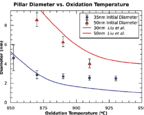
Various models have been investigated to explain the blue shift of the emission peak, shown in Figure 2.42(a,b) as continuous lines. Previous theoretical [276] and experimental [116, 13] work investigated the role of strain in the energy and direct/indirect nature of the silicon band gap. The long axial dimensions introduced uncertainty in the exact location of the emission in the vertical direction.
This allowed the etching to develop vertically at a fixed undercut for the subsequent part of the process. A three-step etching procedure was carried out, where the color of the scheme in Figure 2.50b corresponds to the color of the step in the table. We reported the fabrication and microphotoluminescence characterization of the corrugated silicon quantum dot (SiQD) devices in [366].
The inset shows a similar image with diffraction contrast to highlight the crystalline nature of the remaining silicon nanocrystals. We observed a correlation between the original size of the etched ripples and the peak emission wavelength of the oxidized quantum dot. Alternatively, the sharp peaks observed, particularly in the blue curve in Figure 2.55, may also be influenced by the discrete nature of the experiment.
In the case of nanowires, the single core resulted in a single, extended band gap with a continuous electron channel. This was further complicated by the varying luminescence efficiency as a function of diameter (for example, bulk regions would not provide any luminescence signal at all). The onset of the conduction band is seen as a strong rise in the EELS spectrum in this region.
The core diameter in this range is d) Mesh image of the tail region from EFTEM.
Wafer bonding
Furthermore, the capping layers are preserved over most of the dot surface (only the thin edges become visible during etching), which should maintain carrier confinement within the quantum dot and prevent excessive recombination at surface states. While this may not be ideal for our system, the structure is primarily a result of the MQW being embedded near the center of the cavity layer. In addition to allowing optimal selection of the emitter and passive photonic components independently, these different material systems generally exhibit orthogonal etch chemistry, allowing greater flexibility in the fabrication process.
Therefore, we considered the integration of III-V QWs on wafer-bonded SOI photonics, aiming to use selective QW etching to fabricate III-V QDs directly on the cavity surface. In contrast, the second method couples dot generation to cavity design, requiring the cavity anti-node to exist at the maximum area of the dielectric. For a design that meets this constraint, however, this method has the distinct advantage of being self-aligned and producing a quantum dot located precisely in the center of the largest dielectric region in the cavity.
By carefully commanding the wet etch rate, the exact size (and thus spectrum) of the emitter could also be readily controlled. A cross-section of a similar sample is presented in Figure 2.71a to illustrate the structure, together with the photoluminescence spectra of the bare sample recorded at 10K (Figure 2.71b. After removing the InP, we had to buffer diluted to avoid loading the photonic crystal with excessive dielectric material.
However, completely removing the buffer would destroy the electronic properties of the QW and risk mechanical damage to the thin underlying layers. The overall luminescence efficiency of the cavity-bound and out-of-cavity spectra were essentially identical, but the curves show several notable differences. The abrupt increase in polarized photoluminescence beyond 1550 nm suggests the onset of the semiconductor band of the photonic crystal and its coupling to the continuum of lower frequency guided modes; the shallow increase above 1550 nm in the spectra outside the cavity is likely the result of an unintentional coupling with the nearby resonator, which was located just outside the focus of the excitation beam.
Similarly, the discrete peaks at higher energies are consistent with coupling to acceptor modes of the resonator within the photonic band gap of the mirror region; these features are not visible in the off-cavity data.
Cavity-enhanced optical trapping
At this scale, the influence of the particle on the field profile is minimal, allowing us to determine the trap behavior using only the bare field profile. The time-averaged energy in the resonator, U, is the sum of the electric and magnetic contributions. To maximize coupling, it is usually assumed that the emitter is located at the peak of the electric field.
In general, only a fraction of the total excitation power will be coupled into the cavity due to detuning or modal mismatch. The depth tor stability of an optical trap refers to the potential barrier experienced by the particle and is a measure of the energy difference in the system due to the presence of the particle. This strategy also results in a larger fraction of the energy residing in the primary anti-node.
While stability provides a threshold for particle capture, it does not place any restrictions on particle movement within the trap. Near the steady state, the trap can essentially be modeled as a linear spring. In addition to cQED system optimization criteria, the use of a cavity to improve trapping performance warrants several other considerations.
The peak trapping forces occur just above the center of the cavity, where the electric field reaches its maximum within the cladding3. To accurately calculate the gradients from simulations (whose grid sizes are generally larger than those of a typical nanocrystal), we observed that the mode profile at the center of the cavity is very similar to the fundamental waveguide mode. Figure 2.80 shows an illustration of the trapping depth and |E|~ 2on the trapping surface.
Such structures maintain the tight confinement of the acceptor (dielectric) mode, while access to the true electric field maximum is provided by an inclusion, which eliminates the drop in the electric field at the surface.
![Figure 2.75: Illustrations of the optical trapping setup and diagram of the proposed model from Ashkin’s first demonstration in 1970 [8].](https://thumb-ap.123doks.com/thumbv2/123dok/10409458.0/162.918.385.618.88.215/figure-illustrations-optical-trapping-diagram-proposed-ashkin-demonstration.webp)


![Figure 2.11: Dry oxidation of (100) silicon in the thin film regime, following [235, 234, 233, 232].](https://thumb-ap.123doks.com/thumbv2/123dok/10409458.0/67.918.228.742.102.465/figure-dry-oxidation-100-silicon-film-regime-following.webp)