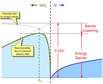
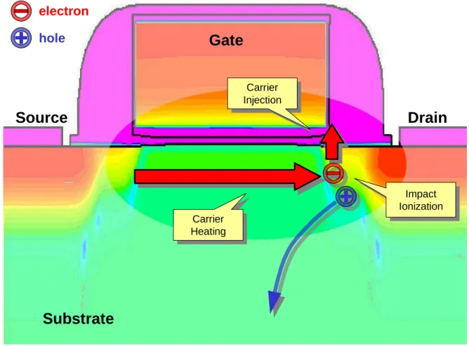
Consequently, the concentration of energy carriers available for injection into the oxide is a strong function of the electric field distribution in the silicon substrate. A charge carrier in silicon near the Si–SiO2 interface produces an opposite charge. An electric field in the oxide near the drain causes the Schottky barrier for holes (but not electrons) to be lowered.
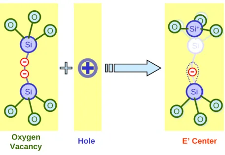
Similarly, exposure to ionizing radiation can be used to generate electron-hole pairs directly in the oxide. Therefore, the resulting degradation in the oxide is also uniform along the channel of the device. Holes trapped near the Si-SiO2 interface have been associated with interface trap generation in such a model [60, 61].
This requires one to simulate not only the injection but also the transport of the injected carriers into the oxide. It is essential to model the transport of carriers in the oxide under such conditions. The presence of mobile charge in the oxide requires the solution of Poisson's equation.
V GS (V)Ig/Igmax
LDDInjected Electron Density (/cm3)
It clearly shows the localized distribution of negative charge increasing in density as we move from the source to the drain, as well as the saturation of the trapped electron density near the drain.
LDDTrapped Electron Density (/cm3)
The pre- and post-voltage drain currents are shown as functions of the gate bias at a drain bias of -0.1 V in Fig. 23, showing an increase in the current after voltage. The increase in the current can be explained as a result of the localized lowering of the threshold voltage due to the trapped electrons in the oxide. 24 shows a plot of the experimental and simulated relative transconductance change with respect to the initial transconductance as a function of the strain time.
The increase in transconductance is due to an apparent channel shortening due to the negative charge in the gate oxide. The degradation of device parameters in n- and p-channel MOSFETs due to hot-carrier injection has been extensively studied previously. The channel lengths of devices used in this part of the study ranged from 0.10 µm to 2.0 µm with oxide thickness of 10 nm and channel width of 10 µm.
In n- and p-channel devices, the dependence of the substrate current on the bias condition provides a direct measure of the rate of impact generation. The relatively slow spatial variation of the electric field in long-channel devices allows one to model the impact generation rate as a function of the local electric field. In particular, hot carrier simulation approaches based on the lucky electron model use an estimate of the maximum channel electric field, Emax to model the substrate current bias dependence using [16]:.
The simulated value of Emax for a 2.0 µm nMOS device as a function of applied gate bias for VDS= 5.0 V is shown in Fig. 48, especially at high electric fields, due to the presence of non-local effects in the carrier- Energy-dependent impact-ionization model in our simulations. This behavior determines the rate of device degradation as discussed in the next section.
E max (V/cm)
1/E max (cm/V)
The influence of hot-carrier-induced interface drop generation is typically measured in terms of variation in linear transconductance, Gm, or the drain current at a specific bias condition. In our simulations, we used the percentage change in maximum transconductance, ∆Gm/Gm0, obtained from IDS−VGS characteristics at VDS=0.1 V as a measure of the build-up of the interface drop. The simulated carrier injection current as a function of the gate bias voltage at VDS= 5.0 V for a device with L=2.0µm is shown in Fig.
Stress Time (seconds)
The accurate modeling of such physical mechanisms is essential to predict the hot-carrier reliability of aggressively scaled MOS technologies. In the case of n-channel MOSFETs, the majority of HC-induced parameter shift is due to the generation of interface traps. The effect of scaling on the hot-carrier reliability of this technology was evaluated using devices with gate lengths ranging from 0.17 µm to 0.35 µm.
However, the presence of this implant may result in increased vulnerability of the hot carrier due to the higher rate of impact generation. Hot carrier degradation of the test structures was evaluated by performing accelerated stress experiments at a drain bias much higher than the normal operating bias for the structures. Since the substrate current is a direct measure of the impact ionization rate in the device, this bias condition corresponds to the maximum impact ionization in the test structures.
During the hot-carrier voltage experiments, the gate bias was maintained at a value that resulted in the maximum substrate current at the corresponding drain bias. The hot carrier-induced device degradation was characterized by monitoring various device parameters during the stress. In the results presented here, the shift in drain current at VDS=VGS=0.9 V is used as a measure of the device degradation.
Device "lifetime" has been defined as the time to 10% change in drain current measured at this bias condition. We begin the modeling process by extracting parameters necessary to accurately model the carrier heating in the silicon substrate. To extract these two parameters, we have used the measured maximum substrate current at the different drain biases used for the accelerated stress experiments, since the substrate current is a direct measure of the shock ionization rate.

Drain Bias (V)
A simulated curve of maximum substrate flow versus outflow was fitted to these data with An and Bn as free parameters. 30 and show that the simulated curve agrees well with the experimental data on the test rigs. The remaining model parameters were taken from values reported in the literature and are listed at the end of this section.
The carrier injection flux and the evolution of the interface trap density distributions along the Si-SiO2 interface during one of these simulations are shown in Figure. It is assumed that there is a uniform energy distribution for the acceptor-type interface states introduced by the interface traps in the silicon bandgap at the Si-SiOTwo interface. Furthermore, the acceptor-type interface states are assumed to be completely distributed in the upper half of the silicon bandgap.
Stress Time (second)
I ds@Vds=Vgs=0.9V
Location Along Si-SiO 2 Interface ( µ m)
Current Density (A/cm2)
Location Along Si-SiO
2 Interface ( µ m)
These parameters were used to simulate the time dependence of the hot-carrier-induced shift in the drain current for several lower drain biases. As seen from this figure, the simulations parameterized to VDS=3.2 V are able to accurately predict the drain-bias dependence of hot-carrier breakdown. It has been shown experimentally that the hot-carrier lifetime of n-channel MOSFETs depends on the supply voltage through the relation [102]:.
Based on this empirical result, we plotted the lifetimes, as defined above, at various drain biases as a function of 1/VDS on a log-linear plot in Fig. As seen here, the simulations are able to reproduce the experimentally observed dependence on drain bias. A similar set of experiments and simulations were performed on devices with gate lengths ranging from 0.17µm to 0.35µm.
The comparison between simulation and experimental data indicates that the hot carrier degradation model scales well with respect to gate length decrease. The degradation for the device with the shortest channel length is slightly overestimated in the simulations. This is also partly an artifact of the interpolation process used to extract the device lifetime at VDS=2 V from the data measured/simulated at higher biases.
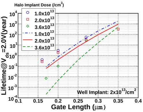
The dependence of the hot carrier lifetime on the doping distribution in the devices is evaluated by comparing the device with different well and halo implants. The results of hot-carrier simulations on devices with three different well and halo implants are compared in Figure. The degradation simulations of hot carriers can predict the dependence of variations in doping profiles for devices with different channel lengths based on extracted parameters. from a single set of devices.
1/Drain Bias (1/V)
Lifetime@V ds=2.0V (year)
Lifetime@V ds=2.0V(year)
Hot-carrier degradation of MOS devices has been investigated as a major reliability problem in recent decades. Empirical and semi-empirical models based on such studies have been used in the past to evaluate the hot-carrier reliability of semiconductor technologies. C0,n A fitting parameter introduced when using a sum of two exponentials to approximate the non-Maxwellian distribution of hot carrier energies, see equation (30).
Weber, “Hot Carrier Degradation of p-MOSFETs in Analog Operation: Significance of Channel Length-Independent Drain Conductance Degradation,” International Meeting on Electronic Devices, p. Yu, “Degradation of RF performance in nMOS transistors due to hot carrier effects,” IEEE Transactions on Electron Devices , vol. Woerlee, “Positive Oxide Charge Generation During Hot Carrier Degradation of a 0.25 µm PMOSFET,” IEEE Electron Device Letters, vol.
On the Mechanism of Generation of Interface Traps in MOS Transistors Due to Channel Hot-Carrier Loading", IEEE Electron Device Letters, vol. Vasi, "Device Scaling Effects on Hot-Carrier Induced Interface and Oxide-Trapped Charge Distributions in MOSFETs" , IEEE Transactions on Electron Devices, vol Ling, "A New Model for Post-Stress Interface Trap Generation in Hot-Carrier Stressed p-MOSFETs", IEEE Electron Device Letters, vol.
Jakumeit, “Full-Band Monte-Carlo Investigation of Hot-Carrier Trends in the Scaling of Metal-Oxide-Semiconductor Field-Effect Transistors,” IEEE Transactions on Electron Devices, vol. Maes, “A consistent model for hot carrier degradation in n-channel and p-channel MOSFETs,” IEEE Transactions on Electron Devices, vol. Maes, “On the different time dependence of interface trap generation and charge trapping during hot carrier degradation in CMOS”, Microelectronic Engineering, vol.
Hu, “The effect of channel hot carrier stress on gate oxide integrity in MOSFETs”, IEEE Transactions on Electron Devices, vol. Hu, “Hot-Carrier Induced Degradation in p-MOSFETs under AC Stress”, IEEE Electron Device Letters, vol.