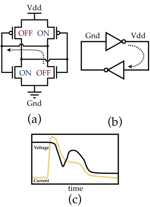
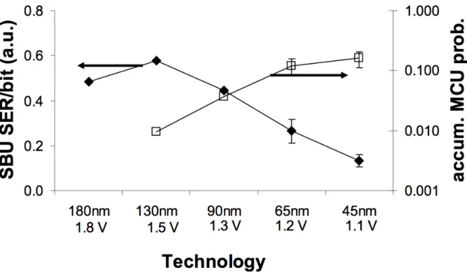
A schematic circuit diagram of an SRAM formed by two cross-. The ON and OFF state devices are labeled for a possible SRAM state. The probability increases from approximately 1% at 130nm feature sizes to 15% on their latest 45nm process.
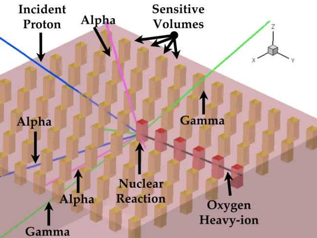
Incident Proton
Nuclear Reaction
Sensitive Volumes
Oxygen Heavy-ion
Alpha
Gamma
That is, the radiation response depends on the orientation of the device relative to the trajectories of the secondary heavy ions. The peak in the current is due to the initial impact of charged particles in the discharge of the device.
OFFOFFON
As the characteristic feature sizes are reduced in state-of-the-art semiconductor processes, MCU continues to increase in probability for SRAM arrays [10, 11]. MCU events are characterized by the bit diversity of the MCU clusters and the dimension of the MCU event.
History
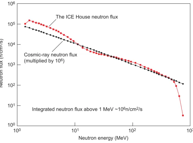
Creating a Neutron Beam Line for Testing Chips and
Electronics
The New Facility
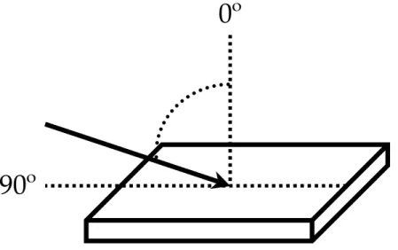
At the largest grazing angle, 90◦, the test board is rotated so that neutrons do not directly impinge on the device surface.
Angle of Incidence (Degrees)
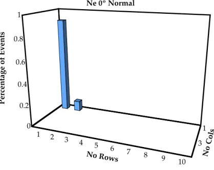
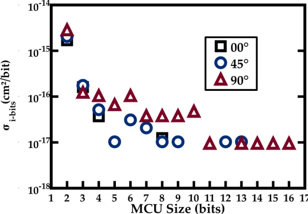
In normal occurrence, 89% of MCU events are two-bit events and only one event greater than three bits is recorded.
MCU Size (bits)
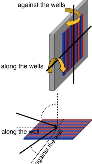
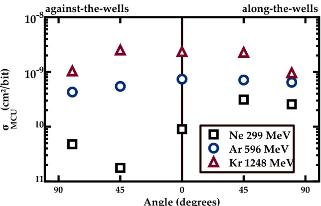
The orientation of the device relative to the neutron beam affects the MCU probability. Y-axis rotation is called "anti-well" because ions incident at these angles are perpendicular to the length of the well. For these cells, the cell height in the direction against the wells is twice the height in the direction along the wells.
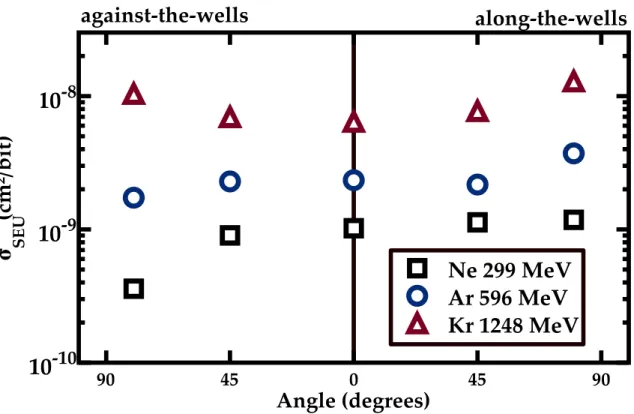
Rotation in the direction of the wells is called "along-well" rotation, while rotation in a perpendicular direction is called "against-well" rotation. bottom). The cross section varies little with angle and orientation for each ion type, except for the slightly ionizing 20Ne at the highest spin angle in the anti-dimple direction.
Angle (degrees)1x10⁻¹⁰
Ne 299 MeV Ar 596 MeV
Device orientation strongly affects the heavy ion response for low LET ions.
Angle (degrees)1x10-11
The probability of causing perturbation in two adjacent cells with two different ions can be approximated by a Poisson distribution. The layout of this particular cell design is approximately twice as long as it is wide and produces a cell pitch in the against-the-wells direction that is twice the cell pitch in the along-the-wells direction. 15 shows the MCU probability for rotation against-the-wells (left) and along-the-wells (right) by Eq.
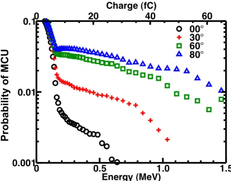
The trajectories of the incident ions at grazing angles are almost parallel to the SRAM array and the ions exchange with more cells, increasing the probability of MCU. The probability is reduced due to the ion's low LET and greater cell thrust in the direction against the wells.
Angle (Degrees)0.01
MeV-cm²/mg 8.6 MeV-cm²/mg
Ar 0º Normal
17 shows the distribution of MCU events for the 40Ar ions at the 79◦ grazing angle with ions incident in the well direction. In the along-wells orientation, the trajectories of the heavy ions are in the direction of the long length of the columns and cross several rows. MCU events in the anti-well direction are smaller than those in the along-well orientation.
These events are smaller because the cell pitch in the against-the-wells direction is double the cell pitch in the other direction. In addition, in the along-the-wells orientation charge can be limited to a single well (refer to Fig. 11).
Ar 79º along-the-wells
Ar 79º against-the-wells
Comparison of all three ions at normal incidence reveals increasing magnitudes and probabilities of MCU events. For heavy ions incident at grazing angles, event sizes increase with increasing LET. Note the difference in the number of affected columns between ions for orientation along the wells.
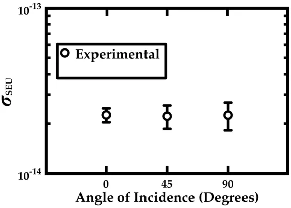
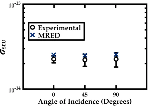
These devices exhibit σSEU that is independent of the orientation of the device with respect to the incident heavy ions. The SEU cross-section is comparable to the total cell area at the lowest LET, implying a device sensitive to charge generation at any point in the cell.
Ne 0º Normal
Kr 0º Normal
Ne 79º along-the-wells
Ne 79º against-the-wells
Kr 79º along-the-wells
Kr 79º against-the-wells
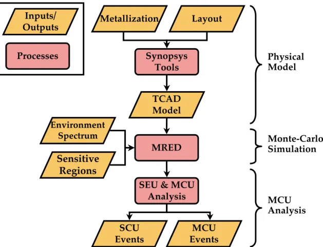
The physical model of the SRAM cell is created using the Synopsys TCAD tool Sentarus [92]. The Sentarus Structure Editor is used to create a physical TCAD model of the SRAM cell. Process emulation is used to create the structure by importing the SRAM cell layout file.
Six layers of copper metal and tungsten vias are included in the physical model of the TI process. If QTotal for the sensitive region of a single SRAM cell is more than this value, MRED counts a disruption of the SRAM cell.
STI STI Si
The trajectories of the incident ions and secondary products are detailed by the colored lines. For each MRED event, MRED's Python interface calls a Python function to post-process each event. At the end of each MRED event, the function call calculates the energy deposited in the sensitive region of each cell and determines QTotal.
The test data presented in those chapters is used to calibrate the simulations and then MRED is used to examine the MCU response for each environment.
BEOL
For each cell, only a single sensitive volume corresponding to the junction of the n-MOSFET transistor in the OFF state was used. The shaded volumes represent the areas in which charge is collected around the sensitive volume of the SRAM cell. The shower of secondary products includes alpha particles, protons, neutrons, gamma rays and a heavy carbon ion.
While the carbon heavy ion is the most ionizing particle, it is the alpha particle that causes the MCU event. The range of an alpha particle is large compared to the range of a heavy carbon ion.
Incident Neutron
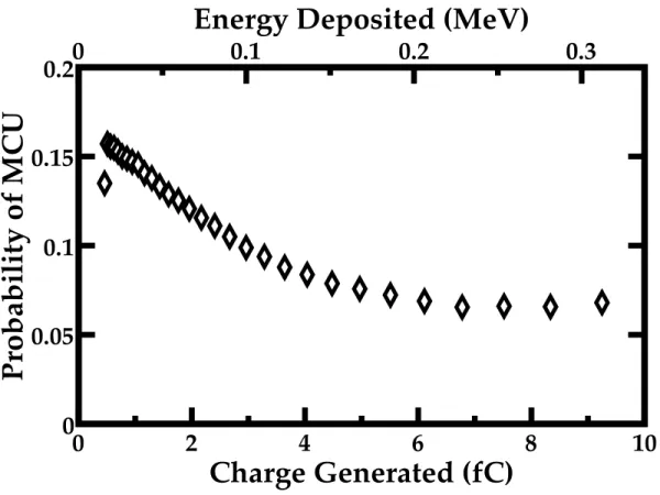
Because the MRED simulation details the amount of energy deposition in each sensitive volume, σSEU can be calculated over a range of deposited energies. In this way, the dependence on deposited energy can be expressed as an energy deposition profile, ED(E), and can be written as Evaluating each event over a discrete set of energies creates a statistical profile of the SCU and MCU in terms of energy deposition.
Energy can be converted into charge, recalling that 3.6 eV of energy is produced by one EHP in silicon. As with the experimental data, σSEU also shows no dependence on the irradiation angle for any value of the critical charge.
Charge Generated (fC)
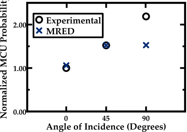
A sufficient number of SEU events, approximately 1000, were recorded during the simulation to increase the count statistics and reduce the error. Error bars represent count statistics for simulation and experimental results and are shown only when visible. At grazing angles, the forward direction is parallel to the matrix surface, increasing the probability that particles will hit more than one cell.
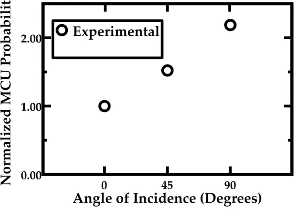
The neutron beam no longer falls on the surface of the device, but on the edge of the test plate. It is unclear what impact this might have on the probability of the MCU, but modeling does not accurately predict the data at this angle.
Energy Deposited (MeV)
The failure rate over time (FIT) is also plotted for sea level operation of 1 Mbit of memory. The neutron-induced FIT rate for sea level operation is calculated from the experimental data of. An error rate of approximately 400 FIT/Mbit for ground level device operation is estimated for the cell, which corresponds to one bit failure every two weeks for a personal computer with one GB of memory, where one byte is equal to eight bits.
1-Bit
2-Bit
3-Bit 4-Bit
Each event was analyzed for SEU, SCU, and MCU using the same criteria as the experimental data. Since the simulations are calibrated to the experimental data, but take into account all angles, particle types and energies, this allows extension of the data set to a realistic space environment. 38 shows the probability of an MCU event in the GEO environment, calculated by eq.
The probability decreases exponentially as event dimensions increase, with nine-line breakdowns accounting for one in every 105 events. While large events are measured during wide-range tests, the probability of these large events in this heavily ionized environment is low.
Energy (MeV/u)
Probability of Event
MCU probabilities for Intel's CMOS processes are shown for various MCU array sizes (i.e., the maximum distance of affected bits in an MCU array). Please note that the maximum neutron- and proton-induced MCU probabilities are of the order of 10%, which is significantly lower than what other groups have reported for even less advanced technologies as discussed in the introduction [12- 14]. However, at energies near the SBU proton threshold (< 25 MeV), proton-induced MCU probabilities are much lower than those induced by the white neutron beam at LANSCE.
Radaelli et al [13] have investigated MCU probabilities as a function of neutron energy and observe double bit decay rates almost independent of neutron energy. If direct ionization dominates, much lower MCU probabilities are expected for vertically incident beams as used in the reported experiments.
F IGURE 5. 45 NM SRAM MCU CLUSTER SIZE DISTRIBUTIONS FOR NEUTRON AND PROTON IRRADIATION
DISCUSSION
34;&K)
Massengill, “Implications of Nuclear Reactions for Test Methods and Analysis of Single Event Effects,” IEEE Trans. Kuboyama, “Investigation of single-ion multibit interference in space experiment onboard memories,” IEEE Trans. Cable, “Effect of ion charge trace size on multibit single-event interference,” IEEE Trans.
Directionality of single event perturbations in 90 nm CMOS due to charge sharing,” IEEE Trans. Smith, “Characterization of multi-bit errors of single-ion traces in integrated circuits,” IEEE Trans. Winokur, “3-dimensional simulation of charge collection and multiple bit distortion in si devices,” IEEE Trans.
Palau, “Monte-carlo simulations to quantify neutron-induced multiple bit disruptions in advanced SRAMs,” IEEE Trans.