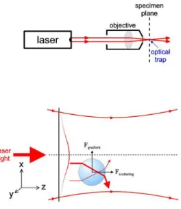
76 Figure 6.13 Illustration of bead displacement relative to the optical traps and definition of forces applied to the beads.
Introduction to low-dimensional materials
Background
- Carbon nanotubes (CNTs)
- Graphene
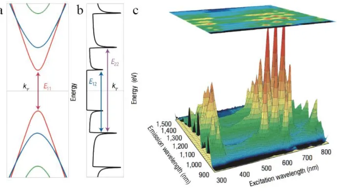
The band structure and density of states of a (19, 0) semiconducting CNT are shown in Figure 1.2a and b, respectively. Together with layered transition oxides, [24, 25] insulator hBN, [26] the common feature of these layered materials is that the bulk 3D crystals are stacked structures of individual layers, as shown in Figure 1.5a.
Electrical properties
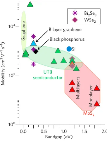
As mentioned in the previous section, 2D materials other than graphene, such as TMDCs, have band gaps that mostly range from 1–2 eV, resulting in a low IOFF and thus a high on/off ratio. For example, a single-layer MoS2 transistor has shown an on/off ratio greater than 104 and a SS less than 80 mV dec-1.[28] However, as a trade-off, the mobility of TMDCs is relatively low, comparable only to silicon.
Optoelectronic properties
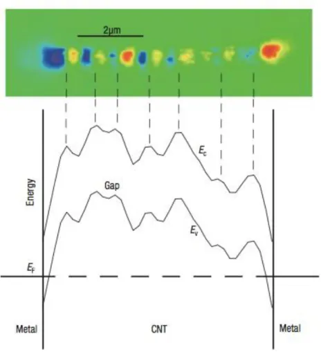
The principle of operation is that photons generate upper-bandgap excitons in the CNT, which can decay into free electrons and holes. When an externally applied bias is used, a change in current (photoconduction) can be observed, while in the other cases a photovoltage is also generated.
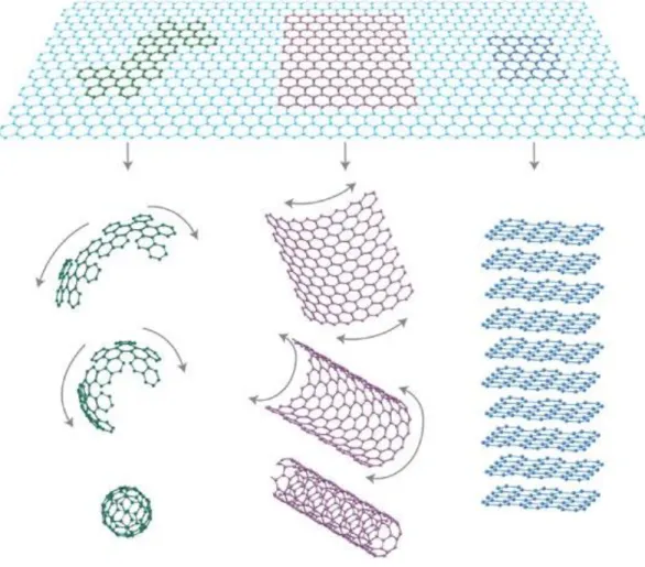
Morphology-induced modifications in graphene nanostructures
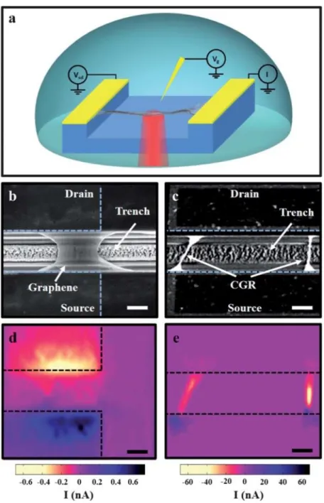
Enhanced photocurrent response in CGRs
The edges of the graphene structure still remain single-layered, as indicated by the white arrows. The corresponding photocurrent images at Vg = 0 V and zero source-drain bias of the suspended single-layer graphene device d and the suspended CGR device e, respectively.
Laser-induced emission from CGRs
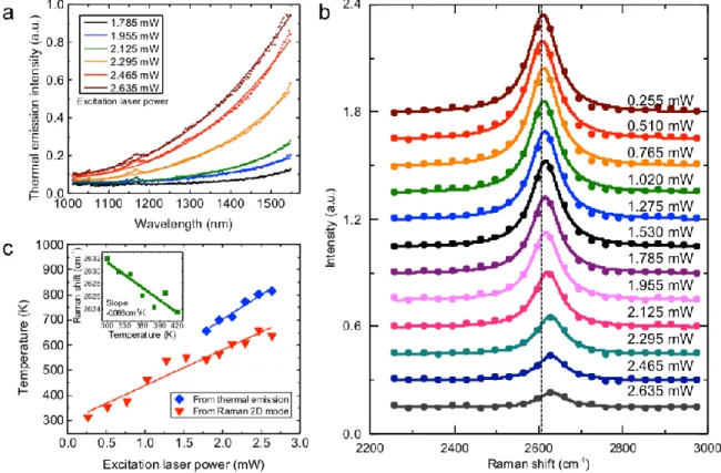
Since the stacked graphene is not a uniform structure, we first determine at a specific region the Raman 2D peak shift with temperature. We obtain the Raman 2D-mode temperature scaling coefficient of -0.066 cm-1 K-1 for the specific region of stacked graphene (Figure 2.4c inset).
Light-matter interactions at metal-semiconductor interface
Metal-semiconductor interface
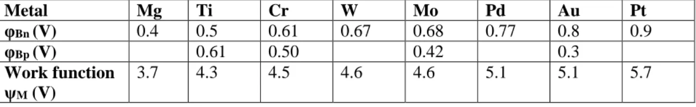
If the contact resistance between the metal and the semiconductor is small, an ohmic contact is formed. Therefore, the semiconductor must be heavily doped and 𝜑𝐵𝑛 must be small to obtain a small contact resistance.
Polarized photocurrent response in black phosphorous FETs
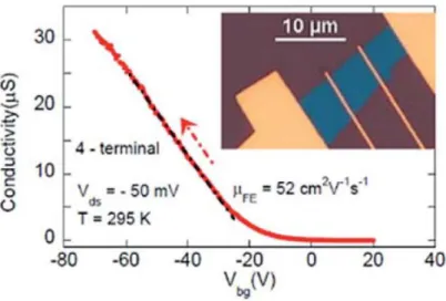
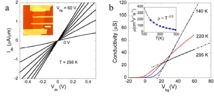
From the slope of the gate-dependent conductance measurement, we estimate the mobility of PB to be 52 cm-2 V-1 s-1. 60 V to 60 V while recording the photocurrent along the channel direction of the BP FET (dashed line in Figure 3.5a), we obtained the gate-dependent scanning photocurrent map (Figure 3.5c). Finally, we estimate the electrostatic potential across the BP flame by bias-dependent photocurrent microscopy.
The local electric field is roughly proportional to the local photocurrent signals in the BP flake. Therefore, we can derive the electrostatic potential along the BP FET by integrating the photocurrent signals.
Photocurrent response at MoS 2 -metal junction
Similar to BP FET, we performed spatially resolved scanning photocurrent microscopy on the same setup (Figure 3.10a) to investigate the local photoresponse at MoS2 metal junctions in high vacuum (1×10⁻⁶ Torr). As shown in Figure 3.11, the edges of the metal electrodes are marked by black dashed lines, and the edges of the MoS2 are marked by blue dashed lines. As shown in Figure 3.12, the maximum photocurrent response at 90o light polarization was observed when lasers with photon energies below the direct band gap of MoS2 (with wavelength of 750 nm or longer).
We take a look at the anisotropy ratio of the photocurrent under different wavelength illumination (Figure 3.13b). Both PVE (650 nm) and surface plasmon (850 nm) induced photocurrent signals have a linear dependence with incident power (Figure 3.13d).
Van der Waals heterostructures
Introduction to van der Waals heterostructures
Electrical properties of BP-MoS 2 p-n heterojunction
Next, a selected BP thin flake was placed on the PDMS stamp on top of a selected MoS2. The thickness of the MoS2 and BP layers are 4.8 nm and 10.0 nm, respectively, as determined by atomic force microscopy. MoS2 and BP flakes exhibit n-type and p-type characteristics at zero gate bias, creating a p-n junction in the overlap region.
When the carrier concentrations in the junction region are adjusted electrostatically by applying a gate voltage, this rectification ratio decreases. Gate-dependent transport properties for BP (red curve, measured between E3 and E4) and MoS2. blue curve, measured between E1 and E2).
Optoelectronic properties of BP-MoS 2 p-n heterojunction
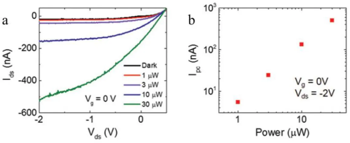
I–V characteristics of BP–MoS2 p–n junction in dark state and under 532 nm laser illumination. At zero gate bias, a p-n junction is formed in the BP-MoS2 heterostructure, leading to strong electron-hole pair separation and remarkable junction photocurrent (Figure 4.4b). The relative contributions of the different photocurrent generation mechanisms are further investigated by polarization-dependent photocurrent measurements in BP-MoS2 p-n.
Compared to the photocurrent signals at the junction region, the photocurrent response at the metal contacts can hardly be identified. We attribute the photocurrent response at the junction to 532nm and 1550nm laser illumination to different photocurrent generation mechanisms.
CNTs for image-guided drug delivery
Functionalization of CNTs
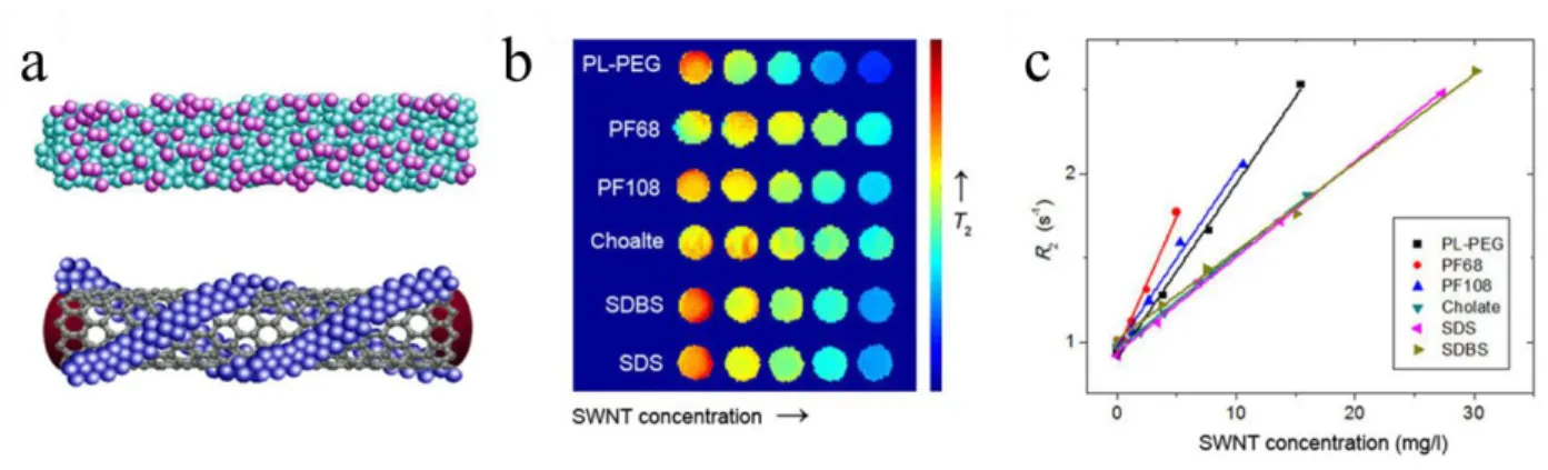
The original sharp absorption peaks observed in the cholate-suspended CNTs became broader and red-shifted toward the peak of PL-PEG-functionalized CNTs (PL-PEG-CNTs). After the four-day dialysis, the NIRF signal of two-step functionalized CNTs was close to that of PL-PEG-CNTs. Despite the gradual change in NIRF during dialysis, the r2 of each sample unexpectedly showed nearly identical values (Figure 5.2c).
Linear fitting revealed that the r2 of CNTs after dialysis was almost identical to that of micelle-encased nanotubes and different from that of PL-PEG-CNTs. The reduction of NIRF quantum yield of two-step functionalized CNTs may largely result from the formation of nanotube bundles, which is typical for PL-PEG-CNTs.
Multi-modality imaging of CNTs
Mammalian brain cells, mainly neurons and glial cells, were prepared as described in the previous literature.[126] For MRI, PL-PEG-CNTs were added to the culture medium at a concentration of 3.56 mg/L and incubated for 24 h. We did not observe any morphological change in cells treated with PL-PEG-CNTs. The final T2 map is shown in Figure 5.4a, and the region of interest was manually drawn to calculate the relaxivity of each sample.
For NIRF imaging, cells were incubated with the PL-PEG-CNTs added culture medium for 72 hours and fixed by 4% paraformaldehyde. Moreover, CNT fluorescence ranging from 1150 to 1700 nm is not absorbed by biomolecules and is easily distinguished from the autofluorescence of biological samples, making it ideal for deep tissue or even whole animal imaging.[127-129] The NIRF of CNT can therefore be used to investigate CNT uptake or labeling in intact brain.
CNTs for drug delivery
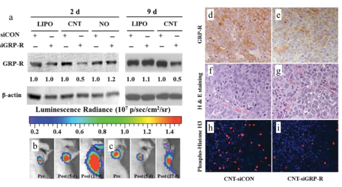
GRP-R expression was significantly silenced by CNT-siGRP-R, compared to commercial transfection reagent LIPO and naked-siRNA. Bioluminescence images were taken for mice treated with CNT-siCON or CNT-siGRP-R; CNT-siGRP-R significantly reduced the tumor size and inhibited the tumor growth. The expression of target GRP-R (brown staining) was significantly reduced in CNT-siGRP-R treated tumor sections.
To validate whether the GRP-R expression was affected in the tumors by CNT-siGRP-R treatment, immunohistochemistry (IHC) was performed. As shown in Figures 5.5h and 5.5i, there were 70% fewer mitotic cells in the CNT-siGRP-R treated tumors than in the CNT-siCON treated.
Carbon nanotube bioelectronics
Introduction to DNA
- Structure
- DNA overstretching
At room temperature DNA molecule in solution is a coiled ball due to their flexible structure. A DNA molecule of length L and persistence length lp, which is the length over which a polymer is roughly straight, is shown in Figure 6.1. DNA response to mechanical force is the cornerstone of the understanding of DNA mechanics, which plays an important role in many genomic processes, such as DNA repair and replication.[137-139] Torsionally unconstrained dsDNA undergoes a structural transition under a tensile force of ~65 pN, where DNA can gain ~70% in contour length over a narrow force range. This process is called overstretching of DNA.
The details of DNA overstretching are key to understanding how DNA interacts with other molecules. Three mechanisms have been proposed to explain the change in force during overstretching: strand exfoliation, localized base-pair breakage, and S-DNA formation. It has been shown that all three of these structures can exist depending on DNA topology and the local stability of DNA.[146] As shown in Figure 6.4, upon application of force, λ-DNA can either form melting bubbles (Figure 6.4a and its corresponding fluorescence Figure 6.4c) or peel off from the notch (Figure 7.4b and its corresponding fluorescence Figure 6.4d).
![Figure 6.2 Different forms of DNA. Image reproduced from Ref. [136].](https://thumb-ap.123doks.com/thumbv2/123dok/10741009.0/74.918.210.708.328.523/figure-different-forms-dna-image-reproduced-ref-136.webp)
CNT transistors in electrolyte
- Electrolyte solutions
- CNT transistors in electrolyte
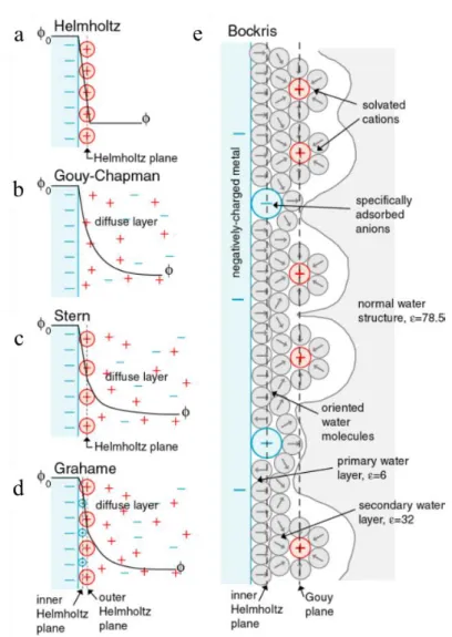
In the Helmholtz model, a single layer of counterions is absorbed to the charged surface and neutralizes its charge, as shown in Figure 6.5a. Other models of the electric double layer include the Stern model (Figure 6.5c) and the Grahame model (Figure 6.5d), both of which combine the Helmholtz model and the Gouy-Chapman model and take both ion size and thermal energy into account. Due to the change of the environment, the noise level of the CNT transistor will also be different.
The charge noise is clearly larger in 5 mM phosphate buffer (PB, Figure 6.6c right) than in air (Figure 6.6c left). The charge noise in the CNT transistor follows the Tersoff model, where ambient noise is dominant in the subthreshold regime. The fluid port fluctuation δV results in the fluctuation in current δIsd (t).
Optical tweezers
These rotations occur in the image plane, which is the back opening of the condenser and inaccessible in a microscope. Therefore, a lens is used to image a photodetector in a plane conjugate to the back focal plane.[163] The axial position of the trapped bead can also be detected using an optical trap. Axial displacements will change the collimation of the laser so that the total amount of light collected by the photodetector changes.
A simple way to obtain the stiffness is to measure the frequency spectrum of the ball with the PSD. The mass of the ball is very small, so its motion can be modeled by a massless, damped oscillator driven by Brownian motion.
CNT and DNA interaction at single molecular level
- The nature of CNT-DNA interactions
- Experimental configuration
- CNT interaction with dsDNA
- CNT interaction with ssDNA-dsDNA hybrid
- CNT morphology change
A dsDNA molecule is attached to the two beads and we slide the dsDNA on top of the CNT. The DNA lies in the perpendicular direction of the CNT, and the CNT lies below the middle part of the DNA. Next, the accurate positions of the beads are calculated, as well as the bead intensities.
Due to the binding between the ssDNA segment and the CNT, the DNA was still attached to the CNT after the centers of the optical trap were above the electrode. Here, we are more interested in the yz-section of the photocurrent images because they can show the bending curves of the CNTs.
Summary and outlook
Increased DNA tension was observed when attached to the CNT, and the binding force between a single DNA base and the sidewall of the CNT was measured. Previous reports on dsDNA interaction with low-dimensional materials mainly focus on nanopores through electrical measurements. It is predicted that ssDNA will exhibit much stronger interactions with CNTs and graphene nanoribbons if no defect is introduced.
The future of low-dimensional materials is promising, but they are still many steps away from real-world applications. With the development of synthesis techniques and the improvement of their unit structures, low-dimensional materials will continue to be strong candidates for electronic and bioelectronic applications.
Fabrication recipe for suspended CNT devices
Growth recipe of suspended CNT devices
Move the boat to the marked position and let it grow there for 20 min for CNT.
Recipe for duplicating pUC-N9 DNA