Magnetic flux density along the X-axis in the as-deposited AlFe protective foil model (µ=100, σ =10000siemens/meter, thickness=2µm) 53 Figure 35. The main biological effect is heating in the electrical wires of an implanted medical device. The temperature rise in the unshielded and shielded wire is calculated from the power loss simulation results.
Therefore, optimal thin film shielding parameters are suggested to keep the heating effects on the wire at acceptable levels.
Introduction
Background of magnetic resonance imaging (MRI)
- Concept for MRI
- Principle of MRI
- Application of MRI
- Effect of MRI on implanted medical devices
2 In the presence of a radio frequency magnetic field, the nuclei of hydrogen atoms can behave like small radio transmitters and emit radio waves as a signal. A septal occlusion device can be implanted into the heart through the femoral vein to treat atrial septal defect (ASD). Strong magnetic fields can induce currents in the pacemaker circuit, causing it to fail and potentially causing the death of the patient wearing the pacemaker.
Another problem occurs when the RF energy from an imaging sequence causes heating in the body's tissues.
Scope of work
- Solution model
- Material investigation
- Computer simulation
- Temperature calculation
In this article, we will concentrate on the power loss produced by the RF magnetic field, which subsequently causes heating of the electrical wiring during MRI. Computer simulations of the shielding effects have been performed and will be discussed in Chapter 3. Shielding is a possible solution to reduce the power loss-related heating effects of the RF magnetic field on the electrical line.
After obtaining the properties of the coated films, we evaluated the electromagnetically induced effects using Maxwell's 2D eddy current solver model in the Ansoft Maxwell EM.5 software package. The thickness, permeability, and conductivity of the insulating material and shielding material are required input data for computer simulations.
Thin Film Deposition and Characterization
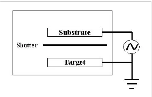
Thin film sputtering deposition
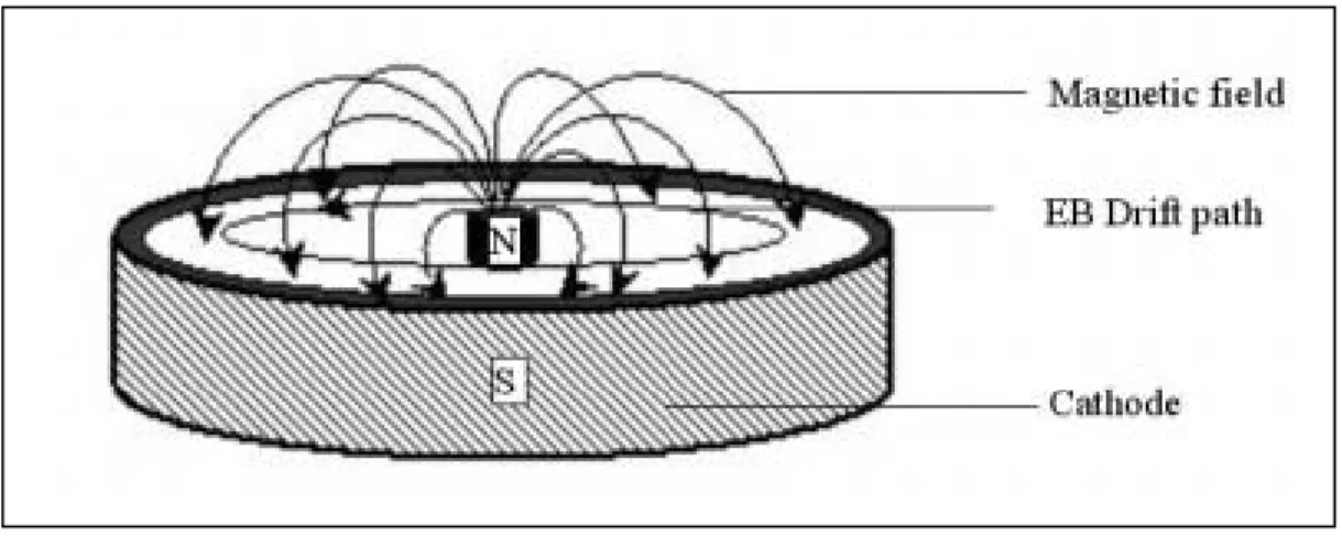
- Sputtering techniques
- DC sputtering
- Pulsed DC sputtering
- RF sputtering
- Magnetron sputtering
- Sputtering modes
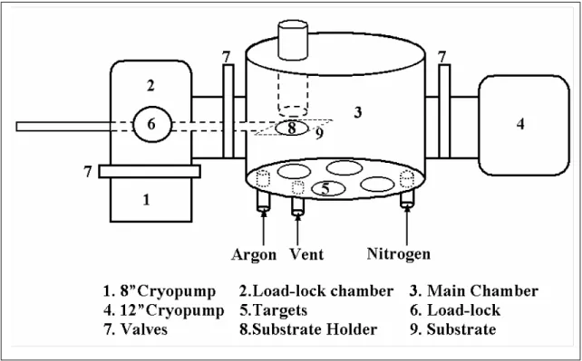
- Sputtering equipment
- Sputtering Deposition Parameters
However, DC sputtering cannot be used to sputter non-conductive targets due to the accumulation of charge on the target surface. By alternating the polarity of the target electrode, net charge accumulation can be eliminated. For non-reactive sputtering, the inert gas, usually Ar, does not directly participate in the formation of compounds on either the target or the substrate.
Nitrogen is used to induce a reaction between the target material and nitrogen to form nitride films.
Thin film characterization
- Thin film analytic methods
- Thickness
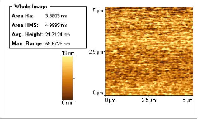
- Roughness of AlN films
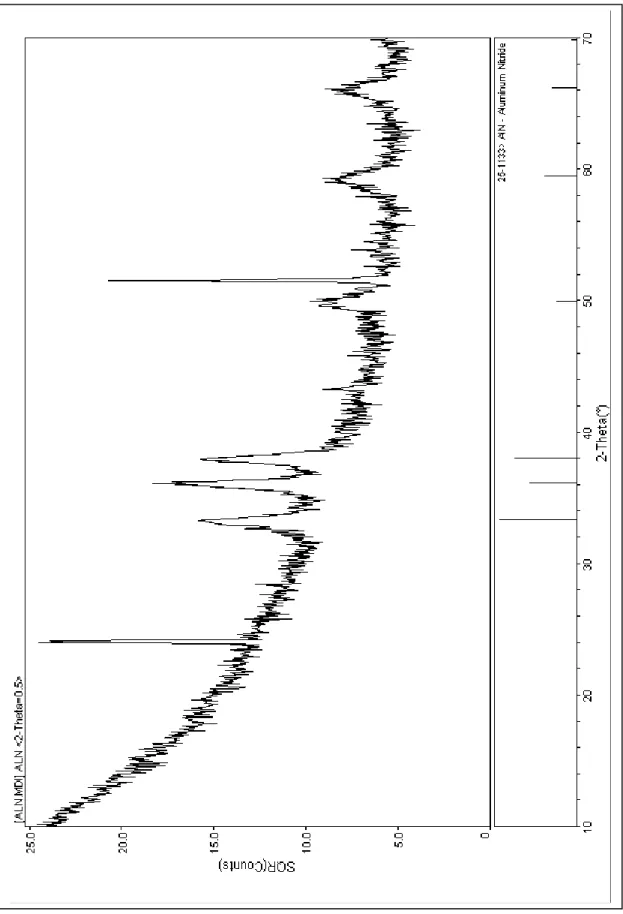
- XRD patterns of AlN and AlFe film
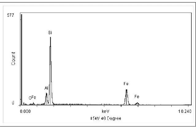
- Energy dispersive X-ray analysis of AlFe film
- Electrical conductivity of AlFe film
- Film stress
- Magnetic permeability
- Hysteresis loop
- Magnetic properties for AlFe films
- Energy distribution in thin films
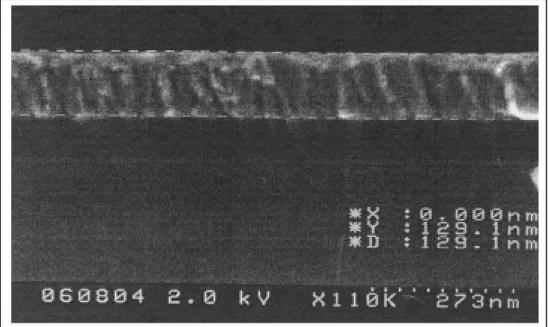
SEM analysis of AlFe film on silicon wafer Figure 9 illustrates the SEM cross-sectional image of AlN. Average roughness (Ra)——The average surface roughness of the average deviation of all points from a plane fitted to the surface of the test part. Root Mean Square Roughness (RMS)——The root mean square average of the measured height deviations taken within the evaluation length or area and measured from the mean linear surface.
After magnetic sputtering deposition, the elemental weight percentage of the deposited AlFe film on the silicon wafer is as follows: Al 42.1 wt%, Fe 57.9 wt%. The electrical conductivity of the shielding material is the required input to the Maxwell 2D eddy current solver. Due to the difference between the coefficients of expansion of the film and the substrate or due to stresses developed during the growth process, films and coatings on substrates may have a residual stress that is either compressive or tensile.
As Figure 15 shows, Line b, the curve in a vacuum, is linear, and the gradient of the curve corresponds to the permeability. When the magnetic field is strong enough to saturate the magnetic moments of the magnetic material, the magnitude of the magnetization reaches its saturation magnetization Ms. For the magnitude of B to return to zero, the direction of the applied magnetic field H must be opposite to that of the initially applied magnetic field direction.
The magnitude of the opposing applied magnetic field which makes the magnetic induction zero is called the coercion, Hc, when B (Hc)=0. The other section is either between 100 and 400 oested or between -100 and -400 oested, which may indicate that the effective magnetic moment at the top of the film is not aligned in the plane of the substrate. For AlFe film with a thickness of approximately 150 nm, a magnetic hysteresis loop measured by VSM at 300K is illustrated in Figure 20.
The percentage of the absorption energy is calculated as one hundred percent minus the percentage of transmission and reflection energies.
Shield basics
Decreases with increasing frequency Decreases with increasing conductivity Decreases with increasing permeability. The final shielding design depends on the following critical factors: anticipated maximum magnetic field intensity, shield geometry, and shielding material properties of conductivity and permeability.
Computer simulation
- Maxwell equations and Maxwell 2D
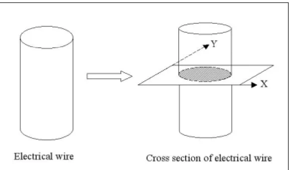
- Geometry definition of electrical wire model
- Radius definition
- No shielding model and shielding model
- Material assignment
- Boundary setup
- Magnetic vector potential
This equation is one of two used by the eddy current solver to calculate A and φ. The structure of the 3D field pattern can be modeled by simulating the fields in the cross-section. Due to the limitation of the software, the radius for the cross-section of the electric wire mode should be chosen carefully.
The radius of the electrical wire model must be greater than the skin depth in the wire induced by the RF magnetic field. Usually, the electrical wire of the implanted medical device is made of aluminum, which has the following parameters:. The black circle in Figure 23 represents the cross-section of the electrical wire, with the radius set to 100 mµ.
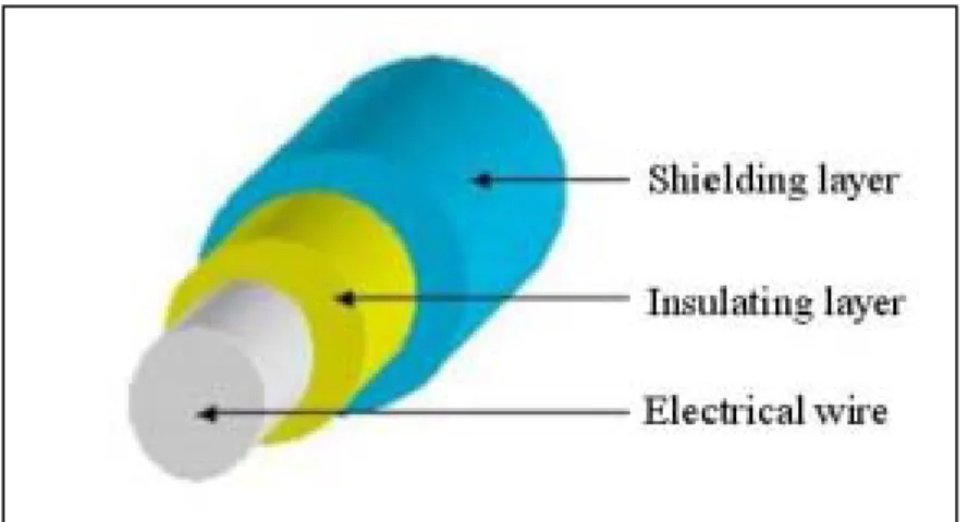
The magnetic film is designed to coat on the surface of the wire for magnetic shielding. The radius of the wire and the size of the human body region remain as constants. Usually, the electric wire in the implanted medical equipment is made of aluminum, so aluminum is assigned as the material of the electric wire, AlN is used as the insulating layer.
We set the right and left edges of the human body as the value limit; therefore the magnetic field touches the boundaries. The vertical distance from the center of the electric wire to the edge of the human body is set at 500.
No shielding model
The magnitude of the magnetic flux density is plotted along the line as Figure 26 shows. As shown in Figure 26, the magnetic flux density can only penetrate a part of the electrical wire (between X= 55 to X= 100). This is because the electrical wire is assigned as aluminum; as a conductor it tends to deflect the magnetic lines of force so that the flux density in the wire becomes smaller.
In the region of the human body surrounding the wire (from X = 100 to X = 500), the magnetic flux density slowly decreases and then reaches.

Shielding model
- Shielding conductivity model
- Shielding permeability model
- Shielding thickness model
- As-deposited AlFe film shielding model
If we compare the magnetic flux density along X in the model without shielding (Figure 26) with the magnetic flux density in the conductive shielding model (Figure 28), we can see that the magnetic flux density in the area of the human body does not change. From Figure 30, we can see that in the area of the human body, the magnetic flux density decreases to 0 tesla. However, the magnetic flux density in the shield is very high (about 0.0083 tesla) due to the high shield permeability value µ=1000.
The magnetic lines of force pass mostly through the shell and flow very little outside it; therefore, the magnetic flux density in the region of the human body becomes smaller. Also the magnetic flux density in the wire region can be almost neglected because the magnetic field strength outside the wire is reduced. Apart from the skin effect, the total magnetic flux density in the wire becomes very small and can be neglected.
In the shielding model with deposited AlFe film, the deposited AlFe film is assigned as the shielding material. The distribution of the magnetic flux in the protective model with an applied AlFe film of thickness 2 um (µ=100) is shown in Figure 33. The magnetic flux density along the X axis in the protective model with an applied AlFe film (µ=100, σ=10000siemens) /meter, thickness =2µm).
The magnetic flux density in the AlFe film is much higher than the originally used value. The magnetic flux density in the human body region near the film surface is lower than in the model without shielding.

Calculation of the heating from power loss
After shielding with the 2um as-deposited AlFe film, the heating in the wire causes the temperature to rise by only 2.8oC. Any pulse sequence may not increase the temperature by more than 1oCelsius.3 In our calculations, the heat dissipation of the AlN and the human body is not taken into account. Since AlN is a very good heat conducting material, the overall temperature rise in the shielded wire must remain within the acceptable level.
Optimal shielding model
Thin film deposition and characterization
Shielding computer simulation
After a certain point (the saturation point), increasing the shielding thickness does not reduce the power loss. As-deposited AlFe film used as the shielding material is simulated to see whether this film can shield the 64MHz RF magnetic field or not. The result shows that the power loss decreased in the wire shielded with the AlFe film compared to that without shielding.
To maintain the elevated temperature within an acceptable level (1oC), the power loss in the wire must be less than 1.26×10⁻⁴Watt/meter. A possible approach is to increase the permittivity of the deposited AlFe film above 280 and keep the thickness at 2 um and the conductivity on the order of 10 4 siemens/meter. This study shows that deposited AlFe can shield part, but not all, of the 64MHz RF magnetic field.
Since the permeability of the AlFe film is related to the percentage of Fe, perhaps we can change the experiment conditions during sputtering to obtain a higher percentage of Fe. The direct relationship between permeability and Fe percentage in AlFe thin film is not clear. According to the shield conductivity model, the conductivity of the film should not exceed 105 siemens/meter, because the increased conductivity will cause an increase in power loss.
When the temperature rise in the wire was calculated from the simulation result, the heat dissipation of the AlN insulating layer and the human body were not considered. Belliveau, "SAR calculations in a realistic and high-resolution model of the head with EEG electrodes in place" Accessed: January, 2003.