Preface
Edward Kolesar, Texas Christian University Stephen Krause, Arizona State University (Tempe) Robert McCoy, Youngstown State University Scott Miller, University of Missouri (Rolla) Devesh Misra, University of Louisiana op. Mark Weaver, University of Alabama (Tuscaloosa) Jason Weiss, Purdue University (West Lafayette) I am also indebted to Joseph P.
List of Symbols
The number of the section in which a symbol is introduced or explained is given in brackets.
S UBSCRIPTS
Coca-Cola, Coca-Cola Classic, the contoured bottle design and the dynamic bar are registered trademarks of The Coca-Cola Company and are used with its express permission.).
2nd REVISE PAGES
HISTORICAL PERSPECTIVE
Only relatively recently have scientists understood the relationships between the structural elements of materials and their properties. This knowledge, acquired over the last 100 years or so, has allowed them to largely shape the characteristics of materials.
Materials Science and Engineering • 3
MATERIALS SCIENCE AND ENGINEERING
REVISED PAGES
WHY STUDY MATERIALS SCIENCE AND ENGINEERING?
A second selection consideration is any deterioration in material properties that may occur during servicing. A material can be found that has the ideal properties, but is prohibitively expensive.
CLASSIFICATION OF MATERIALS
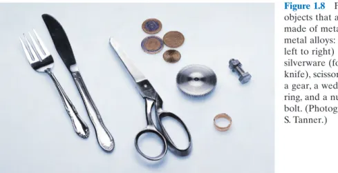
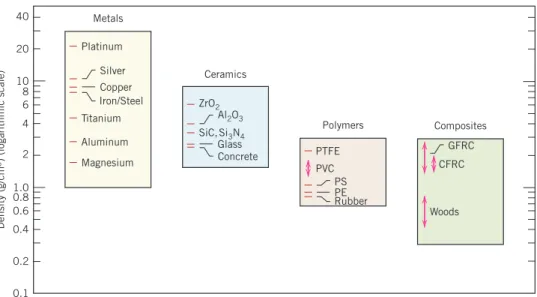
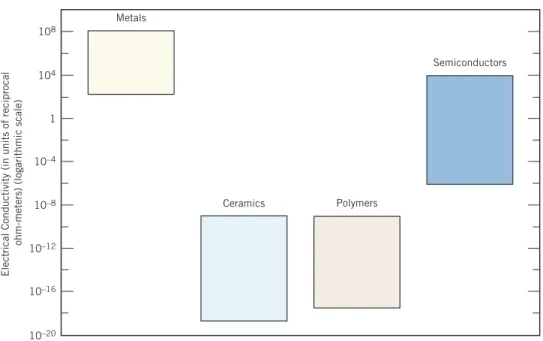
For example, metals are extremely good conductors of electricity (Figure 1.7) and heat, and are not transparent to visible light; a polished metal surface has a shiny appearance. In terms of optical characteristics, ceramics can be transparent, translucent or opaque (Figure 1.2), and some oxide ceramics (eg Fe3O4) exhibit magnetic behavior.
Classification of Materials • 7
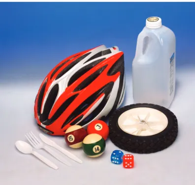
These materials are generally insulating against the passage of heat and electricity (i.e., have low electrical conductivity, Figure 1.7) and are more resistant to high temperatures and harsh environments than metals and polymers. The photo in Figure 1.10 shows several articles made from polymers known to the reader.
Classification of Materials • 9
Glass is impermeable to the passage of carbon dioxide, is a relatively cheap material, can be recycled, but it cracks and breaks easily, and glass bottles are relatively heavy. While the plastic is relatively strong, can be made optically transparent, is cheap and light, and can be recycled, it is not as impermeable to carbon dioxide as aluminum and glass.
ADVANCED MATERIALS
Until recently, the general procedure used by scientists to understand the chemistry and physics of materials has been to begin by studying large, complex structures, and then investigate the fundamental building blocks of these smaller structures. and simpler. This ability to carefully arrange atoms provides opportunities to develop mechanical, electrical, magnetic, and other properties that are not possible otherwise.
MODERN MATERIALS’ NEEDS
We call this a "bottom-up" approach, and the study of the properties of these materials is "nanotechnology"; the prefix “nano” indicates that the dimensions of these structural entities are on the order of a nanometer (109 m)—typically less than 100 nanometers (corresponding to about 500 atomic diameters).5 One example of a material of this type is the carbon nanotube discussed in Section 12.4. Trojan, Engineering Materials and Their Applications, 4th Edition, John Wiley & Sons, New York, 1994.
INTRODUCTION
FUNDAMENTAL CONCEPTS
Sometimes using amu per atom or molecule conveniently; on other occasions g (or kg)/mol is preferred.
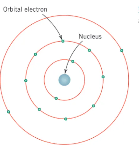
ELECTRONS IN ATOMS
Electrons in Atoms • 17
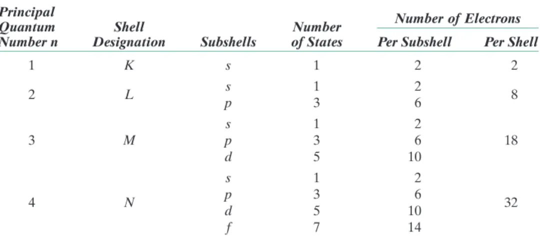
Using wave mechanics, each electron in an atom is characterized by four parameters called quantum numbers. The size, shape, and spatial orientation of an electron's probability density are determined by three of these quantum numbers. The second quantum number, l, stands for the substrate, which is denoted by a lowercase letter—an s, p, d, or f; is related to the shape of the electronic substrate.
Electrons in Atoms • 19
Second, within each shell, the energy of a subshell level is increased by the value of the l quantum number. The shape of the sp3 hybrid is what determines the (or tetrahedral) angle found in polymer chains (Chapter 14).
THE PERIODIC TABLE
The Periodic Table • 23
As can be seen from the periodic table, most elements actually fall under the classification of metals. These are sometimes called electropositive elements, indicating that they can give up their few valence electrons to become positively charged ions.
BONDING FORCES AND ENERGIES
Atoms are more likely to accept electrons when their outer shell is nearly full, and when they are less "shielded" from (i.e. closer to) the nucleus. which is also a function of the interatomic separation, as also shown in Figure 2.8a. The centers of the two atoms remain separated by the equilibrium distance r0, as shown in Figure 2.8a.
Bonding Forces and Energies • 25
Here, the same equilibrium spacing, r0, corresponds to the separation distance at the minimum of the potential energy curve. The magnitude of this binding energy and the shape of the interatomic separation versus energy curve vary from material to material and both depend on the type of atomic bonding.
PRIMARY INTERATOMIC BONDS
For two isolated ions, the attractive energy EA is a function of the interatomic distance according to3. Ionic binding is termed nondirectional; that is, the size of the bond is the same in all directions around an ion.
Primary Interatomic Bonds • 27
For a compound, the degree of either type of bond depends on the relative positions of the constituent atoms in the periodic table (Figure 2.6) or the difference in their electronegativities (Figure 2.7). The wider the separation (both horizontally - relative to Group IVA) -and vertically) from the lower left to the upper right corner (ie, the greater the difference in electronegativity), the more ionic the bond. Conversely, the closer the atoms are to each other (i.e., the smaller the difference in electronegativity), the greater the degree of covalency.
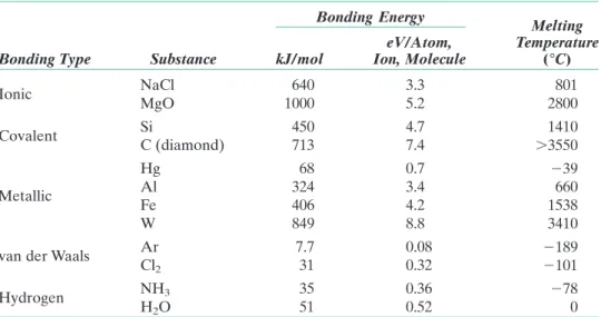
Primary Interatomic Bonds • 29
They can be regarded as belonging to the metal as a whole, or as a "sea of electrons". Some general behaviors of the different material types (i.e. metals, ceramics, polymers) can be explained by the bond type.
SECONDARY BONDING OR VAN DER WAALS BONDING
Conversely, at room temperature, ionically bonded materials are inherently brittle due to the electrically charged nature of their constituents (see Section 12.10). A dipole can be created or induced in an atom or molecule that is normally electrically symmetrical; that is, the overall spatial distribution of the electrons is symmetrical in relation to the positively charged nucleus, as shown in Figure 2.13a.
Secondary Bonding or van der Waals Bonding • 31
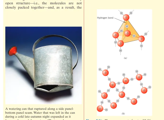
Thus, the hydrogen end of the bond is essentially a positively charged bare proton that is not screened by any electrons. This highly positively charged end of the molecule is capable of a strong force of attraction with the negative end of an adjacent molecule, as shown in Figure 2.15 for HF.
MOLECULES
Furthermore, the magnitude of this coupling will be larger than for induced oscillating dipoles. The size of the hydrogen bond is generally larger than that of other types of secondary bonds and can be as high as 51 kJ/mol (0.52 eV/molecule), as shown in Table 2.3.
Molecules • 33
Write down the four quantum numbers for all electrons in the L and M shells and note which correspond to the s, p, and d subshells. Based on this graph, determine (i) the equilibrium separation between the two ions and (ii) the magnitude of the bond energy E0 between the two ions.
INTRODUCTION
FUNDAMENTAL CONCEPTS
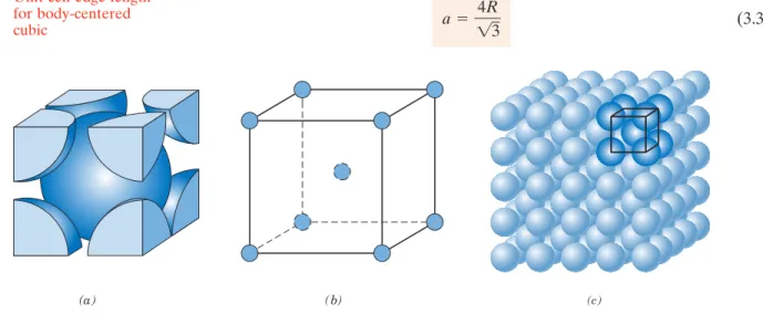
This is called the atomic hard-sphere model in which spheres representing the nearest-neighbor atoms touch each other. An example of the hard sphere model for the atomic arrangement found in some of the common elemental metals is shown in Figure 3.1c.
UNIT CELLS
When describing crystalline structures, atoms (or ions) are viewed as solid spheres with well-defined diameters. Sometimes the term lattice is used in the context of crystal structures; in this sense, "lattice" means a three-dimensional array of points that coincide with atomic positions (or sphere centers).
Metallic Crystal Structures • 41 Convenience usually dictates that parallelepiped corners coincide with centers of
METALLIC CRYSTAL STRUCTURES
The APF is the sum of the sphere volumes of all atoms within a unit cell (assuming the atomic hard sphere model) divided by the unit cell volume. 3.2) For the FCC structure, the atomic packing factor is 0.74, which is the maximum possible packing for spheres all having the same diameter. Another common metal crystal structure also has a cubic unit cell with atoms on all eight corners and a single atom in the cube center.
Metallic Crystal Structures • 43
The coordination number and the atomic packing factor for the HCP crystal structure are the same as for FCC: 12 and 0.74, respectively. Both the total atomic and unit cell volumes can be calculated in terms of the atomic radius R.
DENSITY COMPUTATIONS
APF V S
Density Computations • 45
POLYMORPHISM AND ALLOTROPY
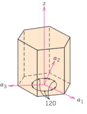
CRYSTAL SYSTEMS
Crystal Systems • 47
This transition from white to pewter gray produced quite dramatic results in Russia in the 1850s. The winter of that year was particularly cold and the record low temperatures lasted for a long time. The uniforms of some Russian soldiers had pewter buttons, many of which collapsed due to these extreme cold conditions, as did many tin church organ pipes. For some crystal systems - namely hexagonal, rhombohedral, monoclinic and triclinic - the three axes are not mutually perpendicular, as in the familiar Cartesian coordinate scheme.
POINT COORDINATES
The coordinate q (which is a fraction) corresponds to the distance qa along the x-axis, where a is the length of the edge of the unit cell. For the unit cell shown in the attached sketch (a), find the point with coordinates 14 1 12.
Crystallographic Directions • 51
Point coordinates for position number 1 are 0 0 0; this position is at the origin of the coordinate system, and as such the edge lengths of the fractional unit cells along the x, y, and z axes are 0a, 0a, and 0a, respectively. The following table shows the cell lengths of fractional units along the x, y, and z axes, and their corresponding point coordinates for each of the nine points in the image above.
CRYSTALLOGRAPHIC DIRECTIONS
The vector as drawn passes through the origin of the coordinate system, so no translation is necessary. The projections of this vector onto the x, y, and z axes are , b, and 0c, which become 1 and 0 with respect to the unit cell parameters (ie, when a, b, and c are dropped).
![Figure 3.6 The [100], [110], and [111] directions within a unit cell.](https://thumb-ap.123doks.com/thumbv2/123dok/10289760.0/75.972.285.450.141.329/figure-directions-unit-cell.webp)
Crystallographic Directions • 53
Conversion from the three-index system to the four-index system,. is realized with the following formulas: Set the indices for the direction shown in the hexagonal unit cell of sketch (a) below.
Crystallographic Planes • 55
CRYSTALLOGRAPHIC PLANES
A discontinuity on the negative side of the origin is indicated by a bar or minus sign positioned above the appropriate index. Thus, in terms of lattice parameters a, b and c, these intersections are and the Reciprocals of these numbers are 0, , and 2; and since they are all integers, no further reduction is needed.
Crystallographic Planes • 57
The plane is marked by lines that represent its intersections with the planes that make up the faces of the unit cell or their extensions. In this figure, for example, the line ef is the intersection between the plane ( ) and the top of the unit cell; likewise the line gh represents the intersection between this same ( ) plane and the plane of the extended face of the lower unit cell.
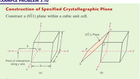
Crystallographic Planes • 59
For crystals with hexagonal symmetry, it is desirable that equivalent faces have the same indices; as with directions, this is accomplished by the Miller-Bravais system shown in Figure 3.7. To determine these Miller-Bravais indices, consider the plane in the figure referred to the parallelepiped marked with the letters A through H at its corners.
LINEAR AND PLANAR DENSITIES
Furthermore, the area of this rectangular section is equal to the product of its length and width. In Figure 3.10b, the length (horizontal dimension) is equal to 4R, while the width (vertical dimension) is equal to , as it corresponds to the edge length of the FCC unit cell (Equation 3.1).
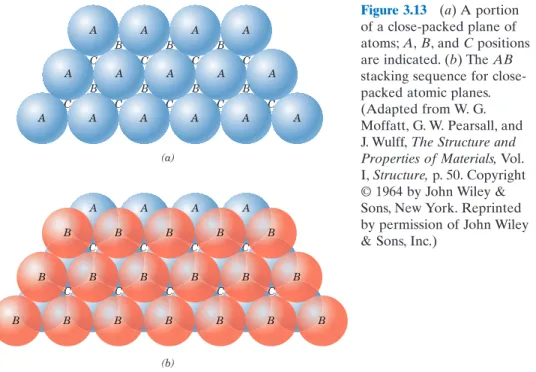
CLOSE-PACKED CRYSTAL STRUCTURES
These close-packed planes for HCP are (0001)-type planes, and the correspondence between this and the unit cell representation is shown in Fig. 3.14. It is more difficult to relate the stacking of close-packed planes to the FCC unit cell.
SINGLE CRYSTALS
The importance of these narrow FCC and HCP planes will become apparent in Chapter 7. Also, the crystal structures of a number of ceramic materials can be created by the stacking of closely packed ion planes (Section 12.2).
POLYCRYSTALLINE MATERIALS
If the ends of a single crystal are allowed to grow without any external constraint, the crystal will assume a regular geometric shape with flat faces, as with some gems; the shape is indicative of the crystal structure. Over the past few years, single crystals have become extremely important in many of our modern technologies, especially electronic microcircuits that use single crystals of silicon and other semiconductors.
ANISOTROPY
In many polycrystalline materials, the crystallographic orientations of individual grains are completely random. Under these circumstances, although each grain may be anisotropic, a sample composed of an aggregate of grains behaves isotropically.
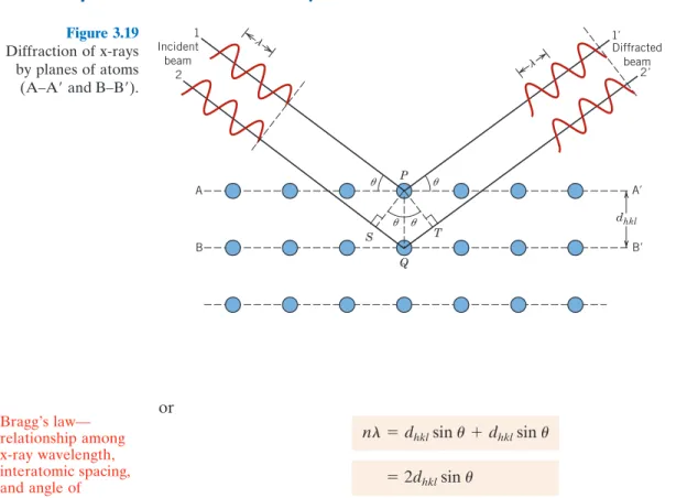
X-RAY DIFFRACTION: DETERMINATION OF CRYSTAL STRUCTURES
81009-type crystallographic direction that is aligned (or nearly aligned) in the same direction, which direction is oriented parallel to the direction of the applied magnetic field. Magnetic textures for iron alloys are discussed in detail in the Essential Materials section of Chapter 20 following the section on X-RAY DIFFRACTION: DETERMINATION OF CRYSTAL STRUCTURES. resulting wave has zero amplitude) as indicated on the far right side of the figure.
Ray Diffraction and Bragg’s Law
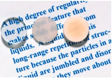
- NONCRYSTALLINE SOLIDS
- Noncrystalline Solids • 71
- INTRODUCTION
- VACANCIES AND SELF-INTERSTITIALS
- Impurities in Solids • 83
- IMPURITIES IN SOLIDS
- SPECIFICATION OF COMPOSITION
- Specification of Composition • 85
- DISLOCATIONS—LINEAR DEFECTS
- Dislocations—Linear Defects • 91
- INTERFACIAL DEFECTS
- Interfacial Defects • 95
- BULK OR VOLUME DEFECTS
- ATOMIC VIBRATIONS
- GENERAL
- General • 97
- MICROSCOPIC TECHNIQUES
- Microscopic Techniques • 99
- Microscopic Techniques • 101
- GRAIN SIZE DETERMINATION
- Grain Size Determination • 103
- INTRODUCTION
- DIFFUSION MECHANISMS
- Diffusion Mechanisms • 111 Figure (a) A copper–nickel diffusion couple
- STEADY-STATE DIFFUSION
- NONSTEADY-STATE DIFFUSION
- Nonsteady-State Diffusion • 115
- Nonsteady-State Diffusion • 117
- FACTORS THAT INFLUENCE DIFFUSION
- Factors That Influence Diffusion • 119 Table 5.2 A Tabulation of Diffusion Data
- Factors That Influence Diffusion • 121
- Factors That Influence Diffusion • 123
- OTHER DIFFUSION PATHS
- INTRODUCTION
- CONCEPTS OF STRESS AND STRAIN
- Concepts of Stress and Strain • 133
- Concepts of Stress and Strain • 135
- Stress–Strain Behavior • 137
- STRESS–STRAIN BEHAVIOR
- Stress–Strain Behavior • 139
- ANELASTICITY
- Elastic Properties of Materials • 141
- ELASTIC PROPERTIES OF MATERIALS
- Elastic Properties of Materials • 143 It next becomes necessary to calculate the strain in the z direction using
- TENSILE PROPERTIES
- Tensile Properties • 145
- Tensile Properties • 147 Inasmuch as the line segment passes through the origin, it is convenient to
- Tensile Properties • 149
- True Stress and Strain • 151
- TRUE STRESS AND STRAIN
- True Stress and Strain • 153
- ELASTIC RECOVERY AFTER PLASTIC DEFORMATION
- COMPRESSIVE, SHEAR, AND TORSIONAL DEFORMATION
- Hardness • 155
- HARDNESS
- Hardness • 157
- VARIABILITY OF MATERIAL PROPERTIES
- Variability of Material Properties • 161
- DESIGN/SAFETY FACTORS
- INTRODUCTION
- BASIC CONCEPTS
- Basic Concepts • 177 Figure The formation of a step on
For example, all curved dislocation positions in Figure 4.5 will have the Burgers vector shown. As shown in the stress-strain diagram (Figure 6.5), the application of the load corresponds to movement from the origin up and along a straight line.