Cells
Thesis by
Dennis M. Callahan Jr.
In Partial Fulfillment of the Requirements for the Degree of
Doctor of Philosophy
California Institute of Technology Pasadena, California
2015
(Defended October 1,2014)
c 2015
Dennis M. Callahan Jr.
All Rights Reserved
for Zhaoxia and little Dylan
Acknowledgements
I would first like to thank my thesis advisor, Harry Atwater, for taking a chance on a kid who took a chance on a school he never thought he could get into. Over the years, his mentorship and constant insight have been incredibly helpful and inspiring.
I would like to thank him for creating an environment where an incoming student with limited scientific knowledge can quickly and efficiently learn and absorb so much about many different areas of research.
I would also like to thank Professors Oskar Painter, Julia Greer, Andrei Faraon and Bill Johnson for serving on my candidacy and thesis committees. I truly appreciate their time and it has been an honor to cross paths with them.
I would like to acknowledge and thank all of the students and post-docs that I have worked with, learned from, and become friends with over the years. I would like to thank Dr. Jeremy Munday for helping me get started on the thin-film GaAs project and for all the time we spent in front of the blackboard thinking about the light trapping limit. Jeremy was also a good friend and I am fortunate to have been assigned to work with him when I started full-time research in the group. I’d like to thank Dr. Jonathan Grandidier for working closely with me for a couple years on the nano sphere solar cell project and for letting me drive the Mustang to MRS in San Francisco. I’d like to thank Dr. Deirdre O’Carroll, the best “Good Cop, Bad Cop” partner one could ask for at MRS poster sessions. I would also like to thank Deirdre for humoring my ideas, trying to (unsuccessfully) make the world’s first Ultrafast Deep Subwavelength Ultra-High Q-Switched Amplifying Nanorod Quantum
Generating Hetero-Metamaterial Lasing Spasing Plasmonic FORABISER, and for the coffee. I’d like to thank Ragip Pala for working on the thin-film GaAs project with me, helping with last-minute EQE measurements, and for always keeping a lighthearted atmosphere. I’d like to thank Dr. Marina Leite for sharing her expertise about semiconductor research with me. I’d like to thank Dr. Koray Aydin for humoring my ideas about metamaterials and for helping me get started with FDTD simulations.
I’d like to thank Dr. Eyal Feigenbaum for teaching me about aspects of optics I had never thought about before. I’d like to thank Dr. Victor Brar for talking about physics, hanging out at the Rath, playing tennis, talking about basketball, and for the single-malt Scotch.
I’d like to thank Raymond Weitekamp for being a good friend, inviting me to his shows, and participating in the short-lived generative art club. Jim Fakonas for being a good friend, lunchtime philosophy discussions and for knowing how to play all my favorite Rolling Stones songs. Ryan Briggs for teaching me about photonics and Purcell Factor. Stan Burgos for cigarettes and deep discussions among wandering homeless men on the streets of San Francisco. I’d like to thank everyone who came to meetings of the short-lived spontaneous emission club. I’d like to thank the spon- taneous emission group from my first group retreat that made it so much fun and for trying to (unsuccessfully) get the term Wanteca into the nano-photonics vernacular (that’s a hybrid waveguide-antenna-cavity). I’d like to thank Colton Bukowsky for all the time and help he has recently given with electron beam lithography and reactive ion etching. For a period, I was working in collaboration with Albert Polman’s group at AMOLF in the Netherlands and I thank them for their contributions, particularly Piero Spinelli.
I’d like to thank the talented undergraduate SURF students I had the privilege of mentoring over various summers including Reggie Wilcox, Clare Chen, Prateek Mantri and Kelsey Whitesell. Kelsey also returned to Caltech for a Masters degree
and I thank her for putting in so much time on the photonic crystal project and for being a good friend.
I’d especially like to thank the Atwater group bluegrass band, Muskrat Water.
This includes Matt “Bayou” Escarra, Dan “Moonshine” Turner Evans, Amanda
“Thunderbird” Shing, Ana “Appalachia” Brown, and Cris “Huckleberry” Flowers.
I reckon jamming with these folks was some of the most fun I had at this here school.
I’d also like to thank Yulia Tolstova for introducing me to The Mountain Goats, The Tiger Lillies and for suggesting I watch The Double Life Of Vernonique by Krzysztof Kieslowski. I’d like to thank Raymond Wietekamp for introducing me to CocoRosie, Bibio and Flying Lotus. I’d like to thank Hal Emmer for introducing me to The Angus And Julia Stone, Carissa Eisler for suggesting I listen to glitch music, and all of Muskrat Water for introducing me to Old Crow Medicine Show.
I’d like to thank everyone who contributed to the LMI-EFRC video contest in- cluding Raymond Weitekamp, Jonathan Grandidier, Emily Kosten, Eyal Feigenbaum, Stanley Burgos and Koray Aydin. I’d like to thank Professor Michael Roukes, Mary Sikora and everyone involved in TEDxCaltech, Feynman’s Vision: The Next 50 Years.
I’d like to thank everyone involved in Caltech’s Art of Science program for creating such a great program and for exhibiting my submissions.
I would like to thank all of my office mates over the years including Amir Safavi- Naeni, Lisa Mauger, Jeff Hill, Alex Krause, Mike Deceglie, Victor Brar, Emily Kosten, and Matt Sheldon. I’d also like to thank the group’s administrative assistants April Neidholdt, Tiffany Kimoto, Jennifer Blankenship, and Lyra Haas.
I would also like to deeply acknowledge Bob Dylan, Tom Waits, David Bowie, Brian Eno, Neko Case and Ryan Adams for providing the bulk of the soundtrack to the last 6 years. I sincerely think I could not have done it without them.
I would like to thank my family for always believing in me and for letting me move 3,000 miles away from home without protest. Lastly and most importantly I would
like to thank my wife, Zhaoxia, for so much more than can be described with words at the end of a paragraph in a thesis. Closing out this chapter of my life, you are the only reason I’ve done any of this.
Dennis M. Callahan Jr.
September 2014 Los Angeles, CA
Abstract
Over the last several decades there have been significant advances in the study and understanding of light behavior in nanoscale geometries. Entire fields such as those based on photonic crystals, plasmonics and metamaterials have been developed, ac- celerating the growth of knowledge related to nanoscale light manipulation. Coupled with recent interest in cheap, reliable renewable energy, a new field has blossomed, that of nanophotonic solar cells.
In this thesis, we examine important properties of thin-film solar cells from a nanophotonics perspective. We identify key differences between nanophotonic de- vices and traditional, thick solar cells. We propose a new way of understanding and describing limits to light trapping and show that certain nanophotonic solar cell de- signs can have light trapping limits above the so called ray-optic or ergodic limit.
We propose that a necessary requisite to exceed the traditional light trapping limit is that the active region of the solar cell must possess a local density of optical states (LDOS) higher than that of the corresponding, bulk material. Additionally, we show that in addition to having an increased density of states, the absorber must have an appropriate incoupling mechanism to transfer light from free space into the opti- cal modes of the device. We outline a portfolio of new solar cell designs that have potential to exceed the traditional light trapping limit and numerically validate our predictions for select cases.
We emphasize the importance of thinking about light trapping in terms of maxi- mizing the optical modes of the device and efficiently coupling light into them from
free space. To further explore these two concepts, we optimize patterns of superlat- tices of air holes in thin slabs of Si and show that by adding a roughened incoupling layer the total absorbed current can be increased synergistically. We suggest that addition of a random scattering surface to a periodic patterning can increase incou- pling by lifting the constraint of selective mode occupation associated with periodic systems.
Lastly, through experiment and simulation, we investigate a potential high effi- ciency solar cell architecture that can be improved with the nanophotonic light trap- ping concepts described in this thesis. Optically thin GaAs solar cells are prepared by the epitaxial liftoff process by removal from their growth substrate and addition of a metallic back reflector. A process of depositing large area nano patterns on the surface of the cells is developed using nano imprint lithography and implemented on the thin GaAs cells.
Contents
Acknowledgements iv
Abstract viii
1 Introduction 5
1.1 Rise Of Nanophotonics . . . 6
1.2 Solar Cell Fundamentals . . . 6
1.3 Current State Of The Art Solar Cells . . . 10
1.4 Why Thin Solar Cells? . . . 10
2 Light Trapping In Thin Film Solar Cells 13 2.1 Single Pass Absorption . . . 13
2.2 Modes Of A Slab . . . 15
2.3 Accessing Trapped Modes . . . 18
2.4 The Ray Optic Light Trapping Limit . . . 20
3 Light Trapping Beyond The Ray Optic Limit 23 3.1 Condition for Exceeding The Ray Optic Limit . . . 25
3.2 Recovering The Ray Optic Limit . . . 28
3.3 Nanophotonic Solar Cell Designs For Exceeding The Ray Optic Light Trapping Limit . . . 29
3.4 What Is The New Limit? . . . 35
3.5 Numerical Demonstration Of Exceeding The Ray Optic Limit . . . . 38
3.6 Planar Waveguide Formulation for Exceeding The Ray Optic Limit . 41
4 Light Trapping With Dielectric Nanosphere Resonators 49 4.1 Dielectric Nanosphere Resonators for a-Si Absorption Enhancement . 50 4.2 Dielectric Nanosphere Resonators for GaAs Absorption Enhancement 58
5 Light Trapping In Ultrathin Film Si With Photonic Crystal Super-
lattices 69
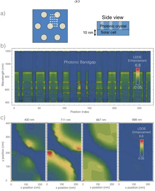
5.1 Introduction . . . 69
5.2 Superlattices In A Square Photonic Crystal . . . 73
5.3 Superlattices In An Optimized Hexagonal Photonic Crystal . . . 80
5.4 Addition Of A Randomly Textured Dielectric Incoupler . . . 82
5.5 Thicker Absorber Layers . . . 84
5.6 Conclusions . . . 85
6 Light Trapping In Thin Film GaAs 87 6.1 Introduction . . . 87
6.2 Epitaxial Liftoff of Ultra-thin Film GaAs . . . 90
6.3 Pattern Optimization and Electromagnetic Simulations . . . 92
6.4 Light Trapping in Ultra-thin Film GaAs Using Nanoimprint Lithography 98 7 Summary And Outlook 106 7.1 Exceeding The Ergodic Limit In Si . . . 106
7.2 Purcell Enhanced Photovoltaics . . . 108
7.3 Photonic Molecules For Light Trapping And Angular Response Engi- neering . . . 112
7.4 Light Absorption Enhancement in Thin Film GaAs . . . 114
Appendices 116
A GaAs Epitaxial Liftoff Procedure 116
B Mesa Etching And Contacting Procedure 120
Bibliography 123
List of Figures
1.1 Current voltage curve for a p-n junction in the dark and under illumination. 8
1.2 Effects of thinning a solar cell on Jsc, Voc, and efficiency. . . 12
2.1 Absorption depth for various photovoltaic materials . . . 14
2.2 Modes of a slab in 3 different representations. . . 16
2.3 Coupling into a slab with a diffraction grating. . . 19
2.4 Shcmatic showing modes of a slab accessed with planar and Lambertian surfaces. . . 21
3.1 Traditional limits to photogenerated current. . . 24
3.2 Potential solar cell architectures. . . 31
3.3 GaP and CdSe slot waveguide LDOS . . . 33
3.4 Photonic Crystal LDOS . . . 35
3.5 Ag nanoantenna LDOS . . . 36
3.6 LDOS Enhancements needed to absorb the entire solar spectrum. . . . 37
3.7 Schematic of spectral reweighting needed to achieve density of states enhancements. . . 38
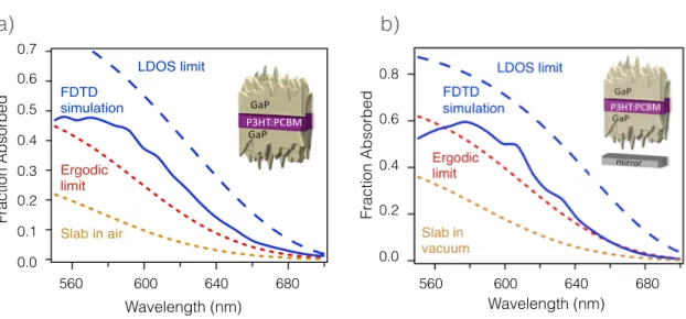
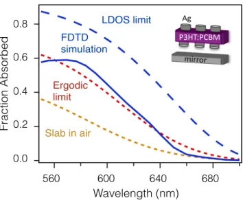
3.8 FDTD simulation of P3HT:PCBM absorber. . . 39
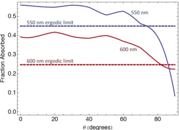
3.9 Angular behavior of the P3HT:PCBM structure that exceeds the ergodic limit. . . 40
3.10 FDTD simulation of P3HT:PCBM absorber with Ag resonators. . . 41
3.11 Waveguide dispersion relations. . . 44
3.12 Plasmonic waveguides that beat the 4n limit. . . 46
3.13 Slot waveguides that beat the 4n2 limit. . . 47
3.14 Absorption for a plasmonic waveguide cladded with a GaP top layer. . 48
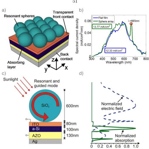
4.1 Dielectric spheres on a-Si. . . 51
4.2 Electric field profiles for dielectric spheres on a-Si. . . 52
4.3 Angular behavior for dielectric spheres on a-Si. . . 55
4.4 Sphere diameter vs. wavelength vs. absorption on a-Si. . . 57
4.5 Current density of a flat GaAs solar cell as a function of thickness. . . 59
4.6 Schematic of a GaAs solar cell with hexagonally close packed SiO2 nanospheres. . . 62
4.7 Behavior of GaAs solar cell with SiO2 nanospheres. . . 63
4.8 Behavior of GaAs solar cell with SiO2 nanospheres. . . 64
4.9 Behavior of GaAs solar cell with SiO2 nanospheres. . . 68
5.1 Conceptual diagram illustrating different degrees of randomness and order. 69 5.2 Absorption spectra of a planar Si layer and photonic crystal. . . 71
5.3 Four different superlattice geometries and their spectral absorption. . . 72
5.4 Absorbed current as a function of superlattice air hole diameter. . . 74
5.5 Field profiles for photonic crystal superlattices. . . 75
5.6 Field profiles for photonic crystal superlattices. . . 76
5.7 TE-TM averaged angular absorption spectra for photonic crystal super- lattices. . . 77
5.8 Integrated angular absorption spectra for photonic crystal superlattices. 78 5.9 Density of states maps of photonic crystal superlattices. . . 79
5.10 Absorption of Suzuki lattice photonic crystals. . . 81
5.11 Integrated absorbed current of Suzuki lattice photonic crystals. . . 82
5.12 TE-TM averaged angular absorption spectra Suzuki lattice photonic crystals. . . 83 5.13 Schematic of superlattice photonic crystal with randomly textured in-
coupler. . . 83 5.14 Thicker superlattice photonic crystals with randomly textured incouplers. 85 6.1 GaAs solar cell device architecture. . . 88 6.2 Images and J-V curve of GaAs device after processing. . . 89 6.3 Sample to sample and cell to cell variation in thin-film GaAs J-V curves
made via epitaxial liftoff. . . 90 6.4 Bilayer anti-reflection coating optimization for GaAs solar cell. . . 91 6.5 Hexagonal TiO2 cylinder FDTD optimization. . . 92 6.6 RCWA simulations of angular response of planar cell and cell with opt-
mized square lattice. . . 93 6.7 AM1.5G spectrally integrated absorbed current for planar anti-reflection
coated cell and TiO2 nanopatterned cell. . . 94 6.8 Electric field intensities for several resonant modes observed in the an-
gular absorption spectrum. . . 95 6.9 Quantification of losses in each layer of the GaAs solar cell structure. . 96 6.10 Angular spectra of the GaAs solar cell with the rear contact removed
with and without addition of an optmized nanopattern. . . 97 6.11 Integrated absorbed current for 4 different GaAs solar cell configura-
tions. . . 98 6.12 1.5 cm x 1.5 cm master and resulting PDMS stamp. . . 99 6.13 Optical image of a hexagonal pattern of TiO2 nanoparticles on Si. . . 100 6.14 SEM images of a hexagonal pattern of TiO2 nanoparticles on Si. . . . 101 6.15 GaAs solar cells after TiO2 nanopatterning and SiO2 deposition. . . . 102
6.16 Current density-voltage curves for cells with and without a TiO2 nanopar- ticle coating. . . 103 6.17 External quantum efficiency measurements of different positions of single
cells with and without nanopatterning. . . 103 6.18 Angle-dependent external quantum efficiency measurements of different
positions of single cells with and without nanopatterning. . . 104 6.19 Short-circuit current as a funtion of angle as determined from EQE
measurements for nanopatterned and AR coated areas of a single cell. . 105 7.1 Thicker superlattice photonic crystals with randomly textured incouplers.107 7.2 Maximum attainable open circuit voltage vs. Purcell Factor. . . 110 7.3 Potential photonic molecule configurations. . . 112 7.4 Assembly of potential photonic molecules by colloidal self assembly. . . 113
Chapter 1 Introduction
World energy consumption is currently above 15 TW, and is expected to increase by 56% by 2040 [1]. The majority of this energy is extracted from a combination of coal, oil and natural gas. These non-renewable resources, while currently dominant, will eventually be depleted. Even before then, continued use of fossil fuels will only worsen the environmental impact of CO2 emissions associated with burning of these energy resources. The earth intercepts about 3.4 million EJ of radiation from the sun each year, about 7,500 times the worlds current energy consumption. This annual solar energy is also an order of magnitude greater than the energy contained in all the worlds estimated fossil fuel reserves and nuclear energy resources combined [2].
However, as of 2010, only about 0.1% of the worlds consumed energy is generated from photovoltaics [3]. No matter how one looks at it, it is obvious that solar energy utilization will have to grow to meet the worlds increasing energy needs. Given these numbers, it also seems inevitable that renewable energy resources like solar will eventually displace fossil fuels as the worlds dominant energy source. In fact, a recent study [2] predicts solar energy (photovoltaic and solar thermal) to provide 70% of world energy generation by 2100. A different study predicts 11% of the worlds total energy needs to come from photovoltaics alone by 2050 [3]. These numbers are based on the sustained growth of the photovoltaics industry over the last decade. In 2012, the world surpassed 100 GW of globally installed PV, and has grown by about 30
GW in each of the last 2 years [4].
To fuel a growing industry such as PV, research and development is needed to reduce the cost per watt of electricity generation. For photovoltaics, this translates to a need for research that reduces the usage of raw materials, reduces the cost of manufacturing and, equally as important, increases energy conversion efficiency. This thesis will explore concepts aimed at achieving these goals using new approaches to light harvesting and device design.
1.1 Rise Of Nanophotonics
In parallel with the development of photovoltaic technology over recent years has been the development of the field of nanophotonics. The unprecedented ability to manipulate and study light on a nano scale has been fueled by recent advances in technology such as electron beam lithography, near field optics, as well as more ad- vanced computer processing power and computation techniques such as finite differ- ence time domain (FDTD) and rigorous coupled wave analysis (RCWA). Entire fields such as those based on photonic crystals [5], plasmonics [6] and metamaterials [7]
have been developed, accelerating the growth of knowledge related to nanoscale light manipulation. This has led to impressive strides in the development of fields such as quantum optics [8], nanoscale lasers [9], near field imaging [10] and others. Despite the continual growth of the closely related fields of photovoltaics and nanophotonics, only recently have they started to merge, giving birth to a rich and interesting new research frontier, that of nanophotonic solar cells [11, 12].
1.2 Solar Cell Fundamentals
The sun can be viewed as a blackbody at a temperature of about 5800 K that con- tinuously emits energy in the form of photons. The energy of these photons can be
harvested in numerous ways, such as through heating of an absorbing material or fluid (i.e. solar thermal), or by taking advantage of the photovoltaic effect in a semicon- ductor and extracting excited charge carriers at a voltage to create electrical power.
While this thesis focuses mainly on photovoltaic devices, the concepts regarding light trapping and absorption are applicable to both areas of solar energy harvesting.
In a photovoltaic device, photons with energy above the material’s bandgap are absorbed, exciting electron-hole pairs that can be extracted as electrical current at an applied voltage to give electrical power. The amount of extracted power divided by the amount of incident power from the sun gives the energy conversion efficiency.
In 1961, Shockley and Queisser calculated the theoretical maximum efficiency of a semiconductor photovoltaic device using the principle of detailed balance [13]. For this calculation, they first considered a photovoltaic device in equilibrium with its surroundings at an ambient temperature, T. This ambient temperature will have an associated blackbody spectrum of ambient photons, some of which the device will absorb. Exactly how many it absorbs depends on the absorptivity, A(ω), of the device, a function of the complex dielectric function of the absorbing material and the geometry. Since the solar cell is in equilibrium, the photons that are absorbed have to be balanced by an outgoing flux of emitted photons. The recombination causing this photon flux constitutes the minimum dark current, Io, of the solar cell.
This current flowing across the junction will increase exponentially when an external voltage is applied, giving the diode equation:
I(V)≈IoeqVkT (1.1)
When the device is placed in a stronger illumination source, such as the sun, a much greater amount of electron hole pairs is excited and the device is no longer in equilibrium. These extra electron hole pairs flow in the opposite direction across the junction and can be collected and extracted as electrical current. Defining the total
amount of photoexcited current IL, this gives a new I-V equation for an illuminated device:
I(V)≈IoeqVkT −IL (1.2)
The resulting dark current-voltage (I-V) curves for a diode in the dark and under illumination are shown in Figure 1.
Figure' 1.1:"(a)" Current" voltage" curve" for" a" p1n" junction" in" the" dark" and" under"
illumination."The"important"solar"cell"parameters"Jsc,"Voc,"FF"and"ef?iciency"can"
be"easily"extracted."
J
scV
ocP
max= J
max* V
maxlight dark
Figure 1.1: Current voltage curve for a p-n junction in the dark and under illumina- tion. The important solar cell parameters Jsc, Voc, FF and efficiency can be easily extracted.
Typically, the current is normalized by the area of the device receiving illumina- tion, and the curent density, J (cmmA2) is used rather than I(A) when describing solar cell devices.
This light J-V curve can be used to define a number of important parameters
widely used to characterize a solar cell’s performance.
1. Jsc or short-circuit current: A measure of how well the solar cell absorbs light.
This will depend on the thickness, geometry of the absorbing material as well as the dielectric function and the light-matter interaction. This is obtained by measuring the collected photocurrent a short-circuit when no voltage is applied to the device.
2. Voc or open-circuit voltage: A measure of how well the device separates charge.
This will first depend on the built-in voltage, a function of the bandgap of the material and the doping levels within the device. Voc will also depend on how much recombination occurs in the device, including radiative and non-radiative channels, which affects the dark current, Jo. The Voc is defined by solving the light J-V curve for V at J = 0 (i.e. the open-circuit condition):
Voc = kT q ln(Jsc
Jo
) (1.3)
3. FF: Corresponds to the squareness of the J-V curve and is defined by F F =
JmaxVmax
JscVoc . This will depend mostly on series and shunt resistances in the device.
These easily obtained parameters can be used to calculate the power conversion efficiency of the solar cell.
η= Pmax
Pinc = JscVocF F
Pinc (1.4)
where Pinc is the incident power density on the device.
1.3 Current State Of The Art Solar Cells
Using the method of Shockley and Quiesser, the maximum theoretical efficiency of a single junction solar cell of any given material can be calculated. All that is needed is an incident spectrum and the bandgap energy of the semiconductor. Two of the most important solar cell materials are Si and GaAs. The maximum efficiency of a single junction Si solar cell under the AM1.5G solar spectrum is about 30%. Currently, the highest achieved efficiency for a Si solar cell is 25% [14]. This efficiency for Si is currently limited by non-radiative recombination processes intrinsic to Si, such as Auger recombination. The thickness of typical record Si devices is usually above 50 microns. A Si record cell could benefit from advanced light trapping by significantly reducing the amount of active material needed, potentially down to below 5 microns, or more than an order of magnitude.
The theoretical maximum efficiency for a GaAs solar cell is about 33%. The current maximum achieved efficiency is 28.8% [14], by Alta Devices [15] using the epitaxial liftoff process of delaminating a thin film of GaAs from its parent substrate and adding a back reflector. All three of the important solar cell parameters are just slightly below their theoretical maximum values. A GaAs cell could benefit from advanced light trapping by reducing the amount of material needed to absorb the spectrum, potentially increasing the voltage by reducing the volume-dependent dark current.
1.4 Why Thin Solar Cells?
Despite the best Si solar cells being many tens of microns thick, the ultimate solar cell is one that is as thin as possible. There are many advantages for thinning the active layer, with the obvious disadvantage that it decreases light absorption. If the exponential reduction in absorption while thinning the cell can be prevented, a solar
cell could gain the following benefits:
• Reduced Cost
The most obvious advantage of a thin solar cell is that is reduces the amount of raw material needed to make the device. As of 2012, about 60% of a Si module cost is due to the Si alone [16]. Reducing the thickness of a Si device by an order or magnitude or more could significantly decrease this cost.
If the solar cell is made from an epitaxial material like a III-V, reducing the active layer thickness will decrease both the amount of precursor gas needed for growth as well as reactor run time for each device. Though direct bandgap materials like GaAs are already relatively thin (∼2-5 microns) compared to Si, their thickness could still in theory be reduced to below a micron, as will be shown in the next section.
• Flexibility
While a crystalline wafer of a semiconductor such as Si or GaAs is extremely brittle and can crack or shatter if handled improperly, a thin film of these materials can be extremely flexible. This opens up many new applications for solar power that otherwise would not be feasible with wafer-based devices.
For example, a flexible module could be rolled out and used when needed as portable charging station, and rolled back up and stored conveniently when not needed. A flexible device could be incorporated into clothing or baggage, wrapped around curved surfaces, or even integrated into the outside of an au- tomobile or aircraft.
• Improved Voc and Efficiency
Perhaps the most intriguing motivation for making a solar cell as thin as possible is an increased operating voltage and possibility of an overall increased efficiency
compared to a thicker device. This is because the dark current density, Jo, is a function of the total recombination within the device. The more bulk material there is in the device, the more bulk recombination and the higher the dark current. This lowers the Voc as shown in Equation 1.3. Plotted in Figure 1.2a is a calculation of the Voc as a function of thickness for a GaAs solar cell with various amounts of bulk non-radiative recombination current. Also shown is how the Jsc decreases with thickness when there is only a single photonic pass. Clearly, in order to take advantage of the increased Voc for thinner cells, significant light trapping is needed to maintain the Jsc of thicker cells. Shown in Figure 1.2b is the calculated efficiency of a GaAs cell with various amounts of light trapping. It can be seen that with increased light trapping, the maximum possible efficiency increases and occurs at thinner and thinner cells. Since both Voc and Jsc need to be maximized to increase efficiency, the ideal solar cell is one that is as thin as possible yet still absorbs the available light from the sun.
0"
0.05"
0.1"
0.15"
0.2"
0.25"
0.3"
0.35"
10" 100" 1000" 10000"
Cell$Thickness$(nm)$
Jsc"Max"(Absorp4vity"="1)"
Ergodic"Limit"
5"Passes"
2"Passes"
1"Pass"
Efficiency
Voc(V)
a) b)
Cell Thickness (μm) Cell Thickness (μm)
Jsc (mA/cm2)
Figure 1.2: a) Effect of thinning a solar cell on Jsc and Voc with no light trapping.
NR is the amount of non-radiative recombination. b) Efficiency as a function of cell thickness with various amounts of light trapping. The more light trapping, the higher the maximum possible efficiency.
Chapter 2
Light Trapping In Thin Film Solar Cells
2.1 Single Pass Absorption
Photons with energy above a semiconductor’s bandgap can be absorbed if given enough time to interact with the material. How quickly light is absorbed depends on the complex dielectric function of the material (i.e. refractive index and absorption co- efficient), and the nature of the light-matter interaction. For light propagating freely as a plane wave in a homogeneous material, the amount absorbed, or intensity I, is exponentially dependent on how far it travels, given by the well known Beer-Lambert law:
I(z) = Ioeαz (2.1)
A commonly used metric for electromagnetic absorption is the absorption depth,
1
α defined as or the depth at which the intensity of a wave decays to 1e (about 35%) of its initial value. Plotted in Figure 2.1 is the absorption depth for some common semiconductors.
A few things are clear from this plot. First, some materials absorb light much more strongly than others. For example, a direct bandgap material like GaAs has a
Figure 2.1: Absorption depth for common photovoltaic materials used in this thesis.
1 10 100 1000 10000 100000 1000000
200 300 400 500 600 700 800 900 1000 1100
Absorption Depth (nm)
Wavelength (nm)
GaAs Si a-Si
Figure 2.1: Absorption depth for common photovoltaic materials used in this thesis.
much shorter absorption depth across the entire spectrum compared to an indirect semiconductor like Si. This will dictate typical thicknesses for each type of solar cell, with GaAs solar cell thicknesses being a few microns and Si thicknesses being many tens or even hundreds of microns. Second, for nearly all materials, the absorption depth is a strong increasing function of wavelength. This has strong implications for light trapping, as the wavelengths that need the most consideration will be the longer ones, and the bandwidth of interest will depend on the thickness of the material.
2.2 Modes Of A Slab
In order to design structures for light trapping, an understanding of the optical modes of a semiconductor slab is critical. Consider a dielectric slab of material with a refractive index, n2, surrounded by an upper dielectric material with index, n1, and a lower dielectric with index n3. Following Yariv [17], we find that different types of electromagnetic modes exist in the slab for a single frequency. Modes that have oscillating field components both inside and outside the slab are known as radiation modes. Modes which are oscillating inside the slab but decay exponentially outside the slab are known as bound or trapped modes. Each of these will be described in more detail below.
The nature of the modes of a slab depends on the relative surrounding refractive indices and a very important quantity known as the propagation constant, β, or in- plane wavevector,k||. It is useful to plot the relationship of wavevector and frequency in a dispersion diagram, as is shown in Fig. 2.2a,d. From this single diagram, we can describe and understand the modes that exist in most photonic structures.
We start with the definition of wavevector for a plane wave propagating in a homogeneous medium:
ω = ck
n (2.2)
where c is the speed of light and n is the refractive index of the material the photon is propagating in. If we define the in-plane wavevector k|| as the component of the wavevector in the plane of the slab, we can start to describe the photon with the dispersion diagram. For a photon propagating inside the incident material with index, n1, it will have a k|| of 0 when it is normal to the plane of the slab. As the incident angle in increased off-normal, it will gain a parallel component dependent on the angle and its frequency:
0 10 20 30 1.2
1.4 1.6 1.8 2
300nm n=3.5 in Air
k|| (um−1)
Photon Energy (eV)
TEo TMo TE1 TM1 Air Lig Slab L TE2
Figure' 2.2:" (top)" Radiation" modes" of" a" slab" represented" (a)" on" a" dispersion"
diagram" (b)" as" electric" 6ield" intensity" as" a" function" of" position" and" ©"
schemcatically" in" terms" of" propagation" angles." (bottom)" radiation" modes"
represented"in"the"same"3"ways."
0 10 20 30
1.2 1.4 1.6 1.8 2
300nm n=3.5 in Air
k|| (um−1)
Photon Energy (eV)
TEo TMo TE1 TM1 Air Lig Slab L TE2
Photon Energy (eV) Photon Energy (eV)
k|| (um-1)
k|| (um-1)
air light line
air light line radiation modes
guided modes
Normalized |E|2
d) e) f)
Normalized |E|2
Figure 2.2: (top) Radiation modes of a 300 nm slab of index n = 3.5 in air represented (a) on a dispersion diagram (b) with ray optics and (c) as electric field intensity as a function of position. (bottom) Guided modes represented in the same 3 ways.
k||=ksin(θ) (2.3)
If the photon is propagating completely in the plane, all of its wavevector will be in the parallel component and it can be described by:
k|| = nω
c (2.4)
This forms what is commonly known as the light line in the dispersion diagram as shown in Fig 2.2a.
Here we can see that as the refractive index of the material of propagation in- creases, the wavevector also increases. This means that the dispersion of photons
propagating in higher indices will appear towards the right on the dispersion dia- gram.
A photon incident on a planar slab at any of these angles will refract at an angle according to Snell’s law, propagate through the slab at that angle, and exit the slab again at an angle according to Snell’s law (at each interface, of course, portions will not only be refracted but also reflected as dictated by the Fresnel equations). This is commonly known as a single pass through the material and would result in minimal absorption if the material were a solar absorber. Adding a back reflector will only add a second pass, with the photon exiting from the top instead of the bottom if it is not absorbed. The set of modes and corresponding in-plane wavevectors associated with this are known as radiation modes and are shown in three different descriptions in Fig 2.2a-c. It is important to note that for a planar interface, these radiation modes are the only modes that can be accesed by photons incident from free space, which only results in 1-2 passes depending on if there is a back-reflector or not.
Photons that gain extra in-plane momentum (k||) can access another set of modes that exist in the slab, called bound modes. These modes can be understood from a ray optics perspective as light trapped by total internal reflection. In the wave optics picture, these modes have oscillating fields within the slab and exponentionally decaying fields outside the slab. These modes will have in-plane wavevectors between the light line of the incident medium and the light line of the bulk medium of the slab, given by ω= ckn
2. They form discreet bands in the dispersion diagram and may have multiple solutions at a single frequency corresponding to different mode orders.
These modes are calculated and shown in Fig. 2.2d-f in 3 different representations for a 300 nm slab with refractive index 3.5 surrounded by vacuum.
A photon or wave in a trapped mode will stay trapped forever unless 1) something changes its momentum (k||) by scattering or diffracting it out of the waveguide or into a different mode or 2) it is absorbed (if the material is absorbing at that wavelength).
Similarly, as stated before, a photon starting out in the lower index incident medium cannot enter one of these trapped modes unless something changes its momentum.
Clearly, a photon trapped in a bound mode (having many effective passes) has a much greater chance of getting absorbed than a photon in a radiation mode (only 1- 2 passes). Getting photons from free space with low in-plane momentum into trapped modes where they can be most efficiently absorbed is the central goal of solar cell light trapping.
2.3 Accessing Trapped Modes
In order for a photon incident from free space to access the guided modes of a slab, its in-plane momentum must be changed so that it matches that of the trapped modes.
A photon can elastically scatter off of a particle that has dielectric contrast with its surroundings if the particle’s size is comparable to the wavelength. This will alter the momentum of the photon and may allow it to couple to nearby optical modes with various momenta. In the wave picture, this occurs because the photon is localized during the scattering event, introducing new, larger k-vectors (modes in k- space are inversely proportional to modes in real space) in the vicinity of the scattering particle [18]. If the particle is close enough to an optical mode (e.g. a guided mode of a slab), and the fields overlap, the energy of the incident wave can be transferred to the optical mode. In the quantum picture, scattering events are described by Fermi’s golden rule, which states that a scattering event will send the scattered particle (i.e.
a photon) into a new state depending on the nearby density of states. As we will see in the next section, a dielectric slab with a higher index than the incident medium has a higher density of optical states than its surroundings, and will preferentially accept photons scattered at the interface between the two media. A single isolated scatterer or a set of random, uncoupled scatterers will ideally redistribute the incident light in
many different directions, or angles from its incident angle.
Figure' 2.2:" (top)" Radiation" modes" of" a" slab" represented" (a)" on" a" dispersion"
diagram" (b)" as" electric" 6ield" intensity" as" a" function" of" position" and" ©"
schemcatically" in" terms" of" propagation" angles." (bottom)" radiation" modes"
represented"in"the"same"3"ways."
0 10 20 30
1.2 1.4 1.6 1.8 2
300nm n=3.5 in Air
k|| (um−1)
Photon Energy (eV)
TEo TMo TE1 TM1 Air Lig Slab L TE2
Photon Energy (eV)
k|| (um-1)
b) Δk=2π
Λ
Λ a)
0 10 20 30
1.2 1.4 1.6 1.8 2
300nm n=3.5 in Air
k|| (um−1)
Photon Energy (eV)
TEo TMo TE1 TM1 Air Lig Slab L TE2
Photon Energy (eV)
k|| (um-1) d)
Δk=2π Λ
Λ c)
k|| = 0
kz k
k|| = k sin(θ) kz
k θ
Figure 2.3: Coupling into a slab with a diffraction grating. The interscting lines in (b) and (d) occur at wavelengths where light can be coupled into guided modes at a given angle. (top) Normal incidence. (bottom) Off-normal incidence.
Another way to access the guided modes of a slab is through diffraction. Diffrac- tion can be viewed as a series of scattering events with the scatterers arranged in an ordered, periodic pattern. In the wave picture, certain angles of propagation are allowed due to constructive interference between the scattered waves, and other an- gles disallowed due to destructive interference. An ordered array of scatterers with period Λ, will add and subtract in-plane momentum from an incident plane wave with values of 2πnΛ , where n is an integer. These new values of in-plane momentum
can also correspond to new angles of propagation given by the diffraction equation:
mλ= Λsin(θm) (2.5)
whereλis the wavelength of light and m is an integer. This is schematically shown in Fig. 2.3a using the dispersion diagram of Fig. 2.2. Light can be coupled into the slab at the locations where the diffraction lines intersect the bands corresponding to the trapped modes of the slab. If the incident angle is changed, the starting value of k|| will change, but the values of added momentum will not. This will only change the resonant wavelengths which couple into the slab as shown in Figure 2.3b. It is important to note that at a given angle, there is only a subset of available modes that can be accessed with a diffraction grating (i.e. the intersecting lines in Fig. 2.3), depending on the period of the grating and the incident angle. Alternately, scattering from single point sources or random surfaces as previously described can potentially couple light into all of the available modes of the slab. If the scattering surface is ideal, it will also do this at all angles. For this reason, random scattering surfaces are typically more useful for broadband, varied angle incoupling for applications such as solar cells.
2.4 The Ray Optic Light Trapping Limit
In 1982, Yablonovitch [19] published a theory describing a fundamental limit to how much light trapping could be achieved in a thin slab of semiconductor with ideal scattering surfaces. This limit is known as the ray optic light trapping limit, also often called the ergodic limit.
Yablonovitch arrives at this limit by considering a homogeneous slab of material with a refractive index, n, and immersing it in a vacuum (with refractive index 1 by definition) that contains blackbody radiation at a temperature, T. When the
radiation inside the slab reaches equilibrium with its surroundings, we can compare energy densities inside and outside the slab:
Uin(r, ω) = n3ω2
π2c3 · 1
e¯hωkT −1 ·¯hω (2.6)
Uout(r, ω) = ω2
π2c3 · 1
e¯hωkT −1·¯hω (2.7) They clearly only differ by a factor of n3.
Absorption is directly related to optical intensity, so by converting the energy density to an intensity by multiplying by the group velocity vg = dωdk and using the well known relation ω= ckn, the intensities become:
Iin(r, ω) = n2
π2c2 · ¯hω3
e¯hωkT −1 (2.8)
Iout(r, ω) = 1
π2c2 · hω¯ 3
e¯hωkT −1 (2.9)
Which differ by only n2. If a simple back reflector is added to add a second pass for any light that escapes the rear of the slab, this intensity enhancement increases to 2n2. After averaging over all angles using a ray optics approach, Yablonovitch comes to an overall absorption, or path length, enchancement of 4n2.
Figure 2.4: (a) modes of a planar slab accessed (grey regions) at all incident angles, (b) modes of a Lambertian textured slab accessed at all incident angles.
Ω
2π 2π
2π (4π w/BR)
a) b)
Figure 2.4: (a) Modes of a planar slab accessed at all incident angles, (b) Modes of a Lambertian textured slab accessed at all incident angles.
An intuitive way to understand where the 4n path length enhancement comes from is by considering the escape cone for light inside the slab. As mentioned pre- viously, a subset of modes known as radiation modes exist inside the slab and can be accessed from free space. If the angle of incident light were swept through all 2π steradians outside the slab as shown in Fig. 2.4, the refracted rays inside the slab would sweep out a cone known as the escape cone. The solid angle, Ω, of this cone is less than the 2π steradians outside because of Snell’s law of refraction and the fact that the index of the slab is higher than free space. Any angles outside of this cone correspond to trapped modes of the slab and cannot be accessed from free space with- out a momentum changing event. Now, consider a slab with perfectly Lambertian textured surfaces. These surfaces will scatter the light ideally into all 4π steradians that exist inside the slab. This ratio of internal angles, or modes accessed, gives the 4n2 light trapping limit.
4π
Ω ≈4n2 (2.10)
by series expansion and trigonometric identity where Ω = 2π(1−cosθ) and θ = sin−1(n1). In this sense, reaching the light trapping limit can be understood as when incident light is able to access all of the modes inside the slab (both radiative and bound).
Chapter 3
Light Trapping Beyond The Ray Optic Limit
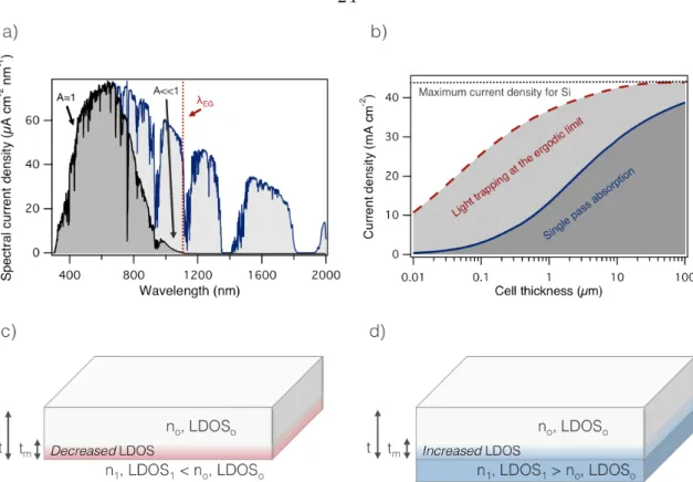
To utilize many of the benefits of ultrathin solar cells, the active layers for most ma- terials have to be reduced to thicknesses where traditional light trapping is no longer effective. At some point, even light trapping that reaches the ray optic, ergodic limit is not enough to generate reasonable short circuit currents, particularly in the wave- length range near the semiconductor bandgap. For any given thickness, there is a range of wavelengths that is near fully absorbed upon 4n2 optical passes and another range that is not fully absorbed due to the exponential nature of the absorption pro- cess and the fact that the absorption coefficient approaches zero at the semiconductor band edge (Fig. 2.1). Therefore we can divide our conceptual approach to the light trapping limit between the spectral region where enhanced absorption is needed and where it is not. The transition region between these two regimes depends on the material properties, thickness, structure, etc.
There is previous evidence that solar cells with non-slablike geometries that op- erate in the wave optic rather than ray optic limit may exceed this limit [20–24], and recent theoretical work has successfully explained the phenomena in selected cases [25, 26]. The theory of Yu et al. establishes a relationship between the modes supported in a slablike solar cell and the maximum absorption attainable but is not easily extensible to the broad portfolio of light trapping schemes currently being ex-
Figure 3.1: Traditional limits to photogenerated current. (a) Current density resulting from AM1.5 solar spectrum absorption for various thicknesses of a bulk slab of Si (inset) assuming either exponential absorption from a single pass or 4n2 passes at the ergodic light trapping limit. (b) Spectrally resolved absorbed current for a 100 nm slab of Si with light trapping at the ergodic limit.
There is a significant region near the band edge where increased light trapping is needed beyond the ergodic limit. (c) A thin slab of semiconductor where the LDOS is affected by a lower index surrounding environment and (d) a higher index surrounding environment..
Figure 3.1: Traditional limits to photogenerated current. (a) Current density resulting from AM1.5 solar spectrum absorption for various thicknesses of a bulk slab of Si (inset) assuming either exponential absorption from a single pass or 4n2 passes at the ergodic light trapping limit. (b) Spectrally resolved absorbed current for a 100 nm slab of Si with light trapping at the ergodic limit. There is a significant region near the band edge where increased light trapping is needed beyond the ergodic limit. (c) A thin slab of semiconductor where the LDOS is affected by a lower index surrounding environment and (d) a higher index surrounding environment.
plored in the literature [11, 21, 27].
We find that a common defining feature of light trapping structures that can ex- ceed the ray optic limit is that the electromagnetic local density of optical states (LDOS) integrated over the active absorber region must exceed that of the corre- sponding homogeneous, bulk semiconductor. That the density of optical states plays an important role in defining the light trapping limit has been alluded to in previous work [25, 28, 29], and we use it here as a defining approach for understanding light trapping. We develop a unified framework for thin film absorption of solar radiation and show that an enhanced integrated LDOS is the fundamental criterion that de-
termines whether light trapping structures can exceed the ray optic light trapping limit, leading to a strategy for design of solar absorber layers with wavelength-scale characteristic dimensions that exhibit optimal light trapping.
3.1 Condition for Exceeding The Ray Optic Limit
As in the original ray optics formulation [19], the electromagnetic energy density serves as a starting point for examining the partitioning of energy between the solar cell and the surrounding environment. For any given geometry, the electromagnetic energy density is a function of position. One way to express the electromagnetic energy density is in terms of the local density of optical states (LDOS), ρ(r, ω), the modal occupation number hνi, and the energy of each mode, ¯hω:
U(r, ω) = ρ(r, ω)· hνi ·¯hω (3.1) The modal occupation number is summed over all modes of the structure. In a homogeneous environment with refractive index, n, and with purely thermal Bose- Einstein occupation, the electromagnetic energy density takes the familiar form:
U(r, ω) = n3ω2
π2c3 · 1
ehωkT¯ −1 ·hω¯ (3.2) By examining the ratio of energy densities inside and outside the solar cell at thermal equilibrium, we can determine the maximum light intensity enhancement and thus the maximum light trapping that is possible [19]. We do this by taking the ratio of electromagnetic energy densities in two distinct cases of interest. This gives an important ratio, that includes the LDOS ratio and the modal occupation number ratio:
U(r, ω)case1
U(r, ω)case2 = ρ(r, ω)case1
ρ(r, ω)case2 · hνicase1
hνicase2 (3.3)
This same ratio can be obtained by starting with an expression for the local absorption rate:
A(r, ω) = 1
2ω·00(r, ω)·E(r, ω)2 (3.4) The absorption can be related to the energy density by rewriting the energy density in terms of the ambient dielectric function and the electric field intensity. In limit of a lossless, dispersionless medium:
U(r, ω) = 1
2(r, ω)·E(r, ω)2+B(r, ω)2
2µ(r, ω) =(r, ω)·E(r, ω)2 (3.5) Equating this with equation 3.1 and rearranging we have for the electric field intensity:
E(r, ω)2 = 1
(r, ω)·ρ(r, ω)· hνi ·hω¯ (3.6) We can insert this into our expression for local absorption rate to determine how the LDOS and modal occupation number affect absorption:
A(r, ω) = 1
2(r, ω)·00·ρ(r, ω)· hνi ·¯hω2 (3.7) Because equations 1 and 4 assume lossless materials, we can only introduce a small amount of absorption before these concepts become ill-defined. It is neverthe- less common to use expressions like this in the limit of low absorption to describe light trapping phenomena, as has been done both in the original derivation [19] and subsequent treatments [25, 26]. We will find next, however, that Eq. 3.7 is not neces- sary but rather has been used to verify the importance of energy density ratios. As
with the expressions for energy density, we can now take the ratio of local absorption rate for 2 distinct cases of interest and again obtain Eq. 3.3.
We can use this ratio to examine numerous cases of interest. In the limit of large thicknesses, we will recover the ray optic light trapping limit for homogeneous mate- rials in Section 3.2. First, we compare a homogeneous absorber with an arbitrarily designed absorber that may be capable of exceeding the ray optic light trapping limit:
ρ(r, ω)case1 ρ(r, ω)case2
· hνicase1 hνicase2
= ρ(r, ω)cell ρ(r, ω)bulk
· hνicell hνibulk
(3.8) where we have assumed integration over all modes of the structure. When an incoupling mechanism fully populates the modes of each structure, the light trapping enhancement is simply the LDOS ratio between the cell structure and a homogeneous bulk structure which achieves the ergodic limit. This implies that if the LDOS of the cell structure is larger than that of a homogeneous medium with the same refractive index, the ergodic light trapping limit can be exceeded. Inputting the expression for LDOS of a homogeneous medium with refractive index n, we reach the condition for exceeding the ergodic limit:
π2c3
n3ω2ρ(r, ω)cell>1 (3.9) assuming that all modes of the structure are fully occupied via an appropriately designed light incoupler, which is often taken to be a Lambertian scattering surface.
We now briefly discuss the importance of fully populating the modes of the arbi- trarily designed solar cell structure. As the ratio of equation 3.8 indicates, a structure with an elevated LDOS is necessary but not sufficient to exceed the light trapping limit, which also depends on the modal occupation numbers. There are numerous examples of solar cell structures that very likely have an elevated LDOS; however, whether or not they have exceeded the traditional light trapping limit has remained
uncertain [20, 23]. Structures that use diffractive elements such as gratings and pho- tonic crystals often couple into only a small subset of the available modes, dictated by momentum conservation. This severely limits the number of modes that are oc- cupied, much like the above-mentioned case of a planar interface. If these structures were integrated with a scattering layer, the full modal spectrum of the device could in principle be excited, and much more light could be absorbed within the solar cell. This would also resolve the relevant problem of limited angular and polarization response associated with many designs. We also note that full modal occupation is not necessary to surpass the ergodic limit, as will be shown below using FDTD calculations.
3.2 Recovering The Ray Optic Limit
Considering first a bulk, homogeneous slab of semiconductor with a planar interface, we find that light incident from all 2 steradians gets coupled into a small subset of the modes within the slab given by the escape cone defined by Snell’s law. We call these radiation modes. We assume that all incident light is transmitted to the solar cell, thus each of these radiation modes is fully occupied with the maximum occupation number defined through the modified radiance theorem [30, 31]. Each incident mode contains an occupation number, νinc, and is mapped into a single radiation mode within the semiconductor defined by Snell’s Law with maximum occupation number νmax = νinc [30, 31]. No more light can be coupled into these radiation modes within the slab as they are fully occupied to the maximum extent dictated by thermodynamics.
There are of course 4π - Ω modes inside the semiconductor left unoccupied in this case, and we call these trapped or evanescent modes [30]. These trapped modes are inaccessible from free space without a momentum changing event such as scattering or diffraction. We count the number of excitations within the slab by multiplying the
number of modes accessed by their occupation number.
We now look at the same slab of semiconductor with a lambertian scattering surface. We assume that this surface does not alter the density of states within the slab as is often assumed [19, 30]. This means that when we take the ratio of equation 3.8, the LDOS terms will cancel, and we will be left considering only the difference in modal occupation numbers. For an incident mode with occupation number νinc, the scattering event splits the energy in this mode between all equal modes within the semiconductor. Thus, each of the internal modes, both radiation and trapped, now have a fraction of this energy, let us say ν4πinc. This means that each of the internal modes can be fed more energy as their occupation numbers are not at their maximum value. We can continue to couple light into the semiconductor until each of these 4π internal modes has an occupation number νmax = νinc. We again count the number of excitations by multiplying the number of modes by their occupation numbers. We can now take the ratio in equation 3.8 for each of these two cases,
ρ(r, ω)lambertian
ρ(r, ω)planar · hνilambertian
hνiplanar = hνilambertian
hνiplanar = 4πhνiinc θchνiinc = 4π
θc ≈4n2 (3.10) where we have assumed integration over all modes of the structure. This gives the traditional, or ergodic, light trapping limit.
3.3 Nanophotonic Solar Cell Designs For Exceed- ing The Ray Optic Light Trapping Limit
We now outline a portfolio of wavelength-scale solar absorber layer designs that ex- hibit an LDOS modified relative to that of a homogeneous slab of the same material.
We begin by examining ultrathin, planar solar cells for which we calculate the LDOS
as a function of position within the semiconductor using the Greens dyadic for a lay- ered planar system [10, 18, 32] and then integrate over position to get the spatially averaged LDOS. For the case of a finite thickness planar absorber, in Fig 3.1c-d, the LDOS modification can be viewed heuristically in terms a slab of thickness t with a homogeneous LDOS (LDOSo) which is modified from its surface to some depthtm by the LDOS of the neighboring material. In Fig. 3.2 we plot this averaged LDOS en- hancement for various absorber structures as a function of thickness and wavelength.
When t >> 2tm, the absorber LDOS modification by the surrounding materials is negligible, but when t ≈ 2tm the change in the absorber layer LDOS due to the in- fluence of surrounding materials becomes significant. First, in Fig. 3.2a we note that the integrated LDOS for a thin semiconductor slab surrounded by free space or lower index materials is always less that that of its corresponding bulk material as the slab thickness is reduced, implying that the light trapping limit in this structure is actually lower than that of the same material in bulk form. This has been pointed out before using a different methodology [30]. However, when the surrounding material includes a metal back reflector as shown in Fig. 3.2b, the integrated LDOS can exceed that of its corresponding bulk material in finite thickness layers, particularly for thicknesses below 200-300 nm. Further, the metal-insulator-metal (MIM) structure shown in Fig.
3.2c exhibits an integrated LDOS enhancement relative to its corresponding bulk ab- sorber material that is very significant for all thicknesses below 500nm, exceeding 50 for all relevant wavelengths with ultrathin layers below 20 nm.
For a two-dimensional planar structure, the modal density of states can be ob- tained from the optical dispersion relations. In this case, the density of guided modes per unit area per unit frequency for the mth mode can be written as [30]:
ρm = km
2π dω
dkm −1
(3.11) where km is the propagation constant. In order to increase the density of modes
Figure 3.2:
Energy (eV)
k(nm-1)
(μm)
Thickness (μm) 1
0.4
400
1.1 1"
0"
0.4 1.2
1.2 3.0
1000
1.1
13
1.7 absorber absorber
metal metal
metal
absorber low index high index high index
Bulk Si
thin Si slab (large
& slow vg) Bulk Si
SPP mode (slow vg)
Bulk n=2 Slot waveguide Bulk Si
(large
& slow vg) Thickness (μm)
1"
0"
Thickness (μm) 1"
0"
Thickness (μm) 1"
0"
228
1
Thickness (μm) 0.1 0.02
550
1
x position (nm) 0 100
6.8
0.05
A
B C GaAs D
A B C D
"0""""""""""""""""""""""""""""2"
"
LDOS"Enhancement"
(a) (b) (c) (d) (e) (f)
1.01.52.02.53.00.0 0.5 1.0 1.5 2.0
Wavelengthnm⇥
Averaged LDOS Enhancement
GaAsPhCSolarCellLDOSEnhancement
k(nm-1) k(nm-1) k(nm-1)
Figure 3.2: Potential solar cell architectures. (a) Planar slab of Si in air in which the LDOS is always below the bulk value. Structures with the potential to beat the ergodic limit: (b) planar slab of Si on an Ag back reflector, (c) Ag/Si/Ag planar structure, (d) high/low/high index structure with refractive indices 3/1.5/3, (e) a photonic crystal with index 3.7, and (f) a split dipole antenna made of Ag with a Si gap. The second row shows the LDOS enhancement (on a log color scale) over the bulk material for each structure for various cell thicknesses and wavelengths. Values of LDOS enhancement > 1 correspond to beating the traditional absorption limit.
For (a - d), the bottom row shows examples of the 2D modal dispersion curves for each structure. The bottom of column e shows that the integrated LDOS enhancement>1 for most wavelengths, and the bottom of column f shows the wavelength dependent LDOS enhancement>1 for radial positions between the split dipole.
above the homogeneous value, eitherkm > k0 orvm = dkdω
m < vo , wherek0 and v0 are the homogeneous values of the propagation constant and group velocity, respectively.
Figure 3.2 also shows for each planar structure examples of the modal dispersion relations, showing regions where the density of states is increased due to either slow (low group velocity) modes or large in-plane propagation constants. Note that these dispersion plot