Paths Towards High Efficiency Silicon Photovoltaics
Thesis by
Hal S Emmer
In Partial Fulfillment of the Requirements for the Degree of
Doctor of Philosophy
California Institute of Technology Pasadena, California
2016
(Defended December 10, 2015)
c 2016 Hal S Emmer All Rights Reserved
To my family
Acknowledgments
First, I would like to thank my advisor, Harry Atwater, for all of his support throughout the course of my PhD. Harry’s enthusiasm and optimism are contagious. He gave me the guidance and support that I needed, and still the freedom to explore and learn independently. This is certainly a delicate balance, but one that Harry has mastered. Additional thanks to my thesis committee, Julia Greer, Keith Schwab, and Bill Johnson, for their help and support throughout my studies.
I am grateful for the students and postdocs who mentored me upon my arrival to the group.
Despite being in the throes of starting a new company, Mike Kelzenberg and Morgan Putnam allowed me to follow them around whenever they were in the lab and ask as many stupid questions as I wanted. I was especially inspired by Mike’s willingness and ability to build the right tool to get a job done, and I kept this approach to solving problems in mind throughout my graduate career.
My early collaborators on the silicon wire project, including Dan Turner-Evans, Adele Tamboli, Emily Warren, Liz Santori, and Shane Ardo, were just as influential. Our regular pizza meetings were a great chance to learn not only about the topic at hand, but also how to design and execute an experiment. You were all helpful in dealing with the ups and downs of silicon wire growth, for both practical and therapeutic reasons.
Thank you to all of my officemates in both Steele 207 (Chris Chen, Sam Wilson, and Jeff Bosco) and Watson 230 (Sunita Darbe, John Lloyd, Siying Peng, Jonathan Grandidier, Seokmin Jeon, and Davis Darvish) for offering help and insightful discussion about science or otherwise.
I would like to give a special thanks to my numerous scientific collaborators. To Michael Deceglie, with whom I worked closely on the silicon heterojunction defect project, thank you for your mentoring and guidance, and helping me learn to integrate simulation and experiment. I was fortunate to be able to work closely with Sisir Yalamanchili on the work involving etched wires. His worth ethic and experimental attitude were inspiring. Dr. Rebecca Saive not only took her time to grow GaP on Si samples, but was also worked closely with me on characterizing devices. She was always eager to share her experience and knowledge in experimental techniques. I have been especially fortunate that all of my scientific collaborators have also been good friends.
My path through grad school followed very closely with that of Chris Chen — from coursework, research on silicon and silicon-germanium wires and III-V on silicon growth, to housing and fantasy
football. He has been a great partner in lab and friend outside.
And of course, thank you to the rest of the Atwater group and Lewis group/JCAP collaborators.
I am grateful that if I needed a hand with anything, or needed someone to tell my why an idea is crazy, there was literally nobody I couldn’t ask. I am also thankful for everyone who helped to take care of equipment in the lab, making it possible to do research at all. And of course, to all my teammates on the A-team.
I would also like to thank the other people who I have encountered in my time at Caltech. The entire Materials Science cohort was a great group, and I would not have learned so much in my classes — or stayed sane — in my first year without you. Marco and Katie remained great friends, and always inspired thought provoking discussions. Thanks go out to all of those who I played GSC sports with or joined me on Alpine club trips for making my time here more enjoyable.
I am grateful for all of my funding sources: BP Solar, the department of energy, under the Sunshot initiative and FPACE projects, and the Bay Area PV Consortium. I would like to thank the NSF and the QESST ERC for funding, but also for so much more. The faculty and students have acted almost as a second committee and group, providing encouragement, support and guidance, as well as friendly faces at the annual retreat and other conferences. I am lucky to have been part of this organization.
Thank you to the numerous staff who make it possible to effectively conduct research. April Neidholdt, Lyra Haas, Jennifer Blankenship, Tiffany Kimoto, Liz Jennings and Lyann Lau — you have all been essential to our group. Christy Jenstad, I think I would still be struggling to schedule my candidacy without you. And thanks for the candy.
I would like to thank the staff of the Kavli Nanoscience Institute, especially Melissa Melendes and Nils Asplund, for all of their support. They not only kept the lab running, but were always available to provide help.
As I reflect on my time here, I owe a special thank you to all of my family on the west coast.
Maxine and Keith, the Benston/Tashmans and Tabb/Steinbergs and of course my new family, the LaZebniks and Summers - you all went out of your way to take me in and make me feel at home, especially around holidays when I couldn’t make the trip back east. This made my time here much more comfortable and enjoyable.
Thank you to my parents, grandparents and aunts and uncles for not completely disowning me for moving to California and making you come here for my wedding.
And of course, last but not least, my wife Emma. Thank you for your unwavering support and believing in everything that I do. I wouldn’t be here now, or the person I am, without you.
Abstract
While photovoltaics hold much promise as a sustainable electricity source, continued cost reduction is necessary to continue the current growth in deployment. A promising path to continuing to reduce total system cost is by increasing device efficiency. This thesis explores several silicon-based photovoltaic technologies with the potential to reach high power conversion efficiencies.
Silicon microwire arrays, formed by joining millions of micron diameter wires together, were de- veloped as a low cost, low efficiency solar technology. The feasibility of transitioning this to a high efficiency technology was explored. In order to achieve high efficiency, high quality silicon material must be used. Lifetimes and diffusion lengths in these wires were measured and the action of various surface passivation treatments studied. While long lifetimes were not achieved, strong inversion at the silicon – hydrofluoric acid interface was measured, which is important for understanding a com- mon measurement used in solar materials characterization. Cryogenic deep reactive ion etching was then explored as a method for fabricating high quality wires and improved lifetimes were measured.
As another way to reach high efficiency, growth of silicon-germanium alloy wires was explored as a substrate for a III-V on Si tandem device. Patterned arrays of wires with up to 12% germanium incorporation were grown. This alloy is more closely lattice matched to GaP than silicon and allows for improvements in III-V integration on silicon.
Heterojunctions of silicon are another promising path towards achieving high efficiency devices.
The GaP/Si heterointerface and properties of GaP grown on silicon were studied. Additionally, a substrate removal process was developed which allows the formation of high quality free standing GaP films and has wide applications in the field of optics.
Finally, the effect of defects at the interface of the amorphous silicon heterojuction cell was stud- ied. Excellent voltages, and thus efficiencies, are achievable with this system, but the voltage is very sensitive to growth conditions. We directly measured lateral transport lengths at the heterointerface on the order of tens to hundreds of microns, which allows carriers to travel towards any defects that are present and recombine. This measurement adds to the understanding of these types of high efficiency devices and may aid in future device design.
Contents
Acknowledgments iv
Abstract vi
1 Introduction 1
1.1 Introduction . . . 1
1.2 Photovoltaic Device Operation and Performance . . . 2
1.2.1 Open Circuit Voltage . . . 2
1.2.2 Short Circuit Current . . . 4
1.2.3 Fill Factor . . . 5
1.3 Past, Present, and Future . . . 5
2 Advances in Silicon Microwire Photovoltaics 7 2.1 Introduction . . . 7
2.2 In Situ Phosphorus Doping . . . 9
2.3 In Situ Junction Formation . . . 10
2.3.1 Growth of Wires with In Situ Junctions . . . 11
2.3.2 Measurements of In Situ Junctions in Single Wires . . . 12
2.4 Material Quality Measurements . . . 18
2.4.1 Light Beam Induced Current with Chemical Passivation . . . 18
2.4.2 Lifetime Measurements . . . 21
2.4.2.1 Motivation . . . 21
2.4.2.2 Measurement . . . 22
2.4.2.3 Results . . . 23
2.4.3 Summary and Discussion . . . 24
2.5 High and Low Temperature Growth . . . 24
2.5.1 Low Temperature Growth . . . 25
2.5.2 High Temperature Growth . . . 26
2.6 Conclusions and Outlook . . . 28
3 Silicon Germanium Alloy Microwires 29
3.1 Introduction . . . 29
3.2 Growth . . . 30
3.2.1 Reactor Modifications . . . 30
3.2.2 SiGe Growths . . . 32
3.3 Characterization and Discussion . . . 33
3.3.1 Compositional . . . 33
3.3.2 Morphology and Growth Rate . . . 34
3.3.3 Doping . . . 35
3.3.4 Optical . . . 37
3.4 Conclusions and Outlook . . . 38
4 High Efficiency with Microstructured Devices 41 4.1 Introduction . . . 41
4.2 Limiting Efficiency Calculations . . . 42
4.2.1 Method . . . 42
4.2.2 Results . . . 43
4.2.3 Summary . . . 45
4.3 Experimental . . . 46
4.3.1 Wire Fabrication . . . 46
4.3.2 Lifetime Measurements . . . 47
4.3.3 Absorption Measurements . . . 50
4.4 Conclusions and Outlook . . . 51
5 Silicon-Gallium Phosphide Heterojunctions 53 5.1 Introduction . . . 53
5.2 Design and Simulation of Gallium Phosphide Heterojunction Devices . . . 54
5.2.1 Interface Defects . . . 55
5.2.2 Band Alignment . . . 56
5.3 Lifetime measurements of Silicon with Gallium Phosphide films . . . 58
5.4 Substrate Removed Gallium Phosphide Films . . . 60
5.4.1 Motivation . . . 60
5.4.2 Substrate Removal Process . . . 62
5.4.3 Electrical Measurements . . . 67
5.4.4 Optical Measurements . . . 68
5.4.5 Time Resolved Photoluminescence . . . 69
5.4.6 Material Characterization of Substrate Removed Films . . . 72
5.5 Silicon-Gallium Phosphide Heterojunction Devices . . . 73
5.6 Conclusions and Outlook . . . 77
6 Lateral Transport in Silicon Heterojunction Solar Cells 78 6.1 Introduction . . . 78
6.2 Simulation . . . 79
6.3 Experimental . . . 80
6.3.1 Current Splitting Between Two Contacts . . . 81
6.3.2 Lateral Transport Near a Defect . . . 82
6.4 Discussion . . . 85
6.5 Conclusions and Outlook . . . 87
7 Future Directions 88 7.1 Materials for Photovoltaics . . . 88
7.2 Device Design . . . 89
7.3 Solar Grid Integration . . . 90
7.4 Conclusion . . . 90
A PECVD Deposition and Characterization 98 A.1 n+ doped amorphous silicon in PL4 . . . 98
A.2 Oxide in PL5 . . . 101
B Transient Simulations using Sentaurus TCAD 103
C Excel VBA Code for Limiting Efficiency Calculations 112
List of Figures
1.1 Breakdown of balance of systems costs . . . 2
1.2 Idealized Current-voltage Characteristics . . . 3
2.1 Schematic of radial and axial junction wire devices . . . 8
2.2 Phosphine doping calibration . . . 10
2.3 Attempt at in situ junction growth with a pause to purge the base dopant . . . 13
2.4 Measurements of an as grown situ junction device . . . 15
2.5 Current-voltage characteristic of surface etched situ junction . . . 15
2.6 Measurements of silicon nitride passivated in situ junction device . . . 16
2.7 Measurements of amorphous silicon passivated in situ junction device . . . 17
2.8 Dark IV curves of in situ junctions . . . 17
2.9 Light beam induced current measurement of . . . 19
2.10 Light beam induced current measurements of wires passivated with buffered hydroflu- oric acid . . . 20
2.11 Schematic of microwave detected photoconductivity decay setup . . . 22
2.12 Lifetime trends with injection level . . . 23
2.13 Silicon wire growth performed at 900◦C . . . 25
2.14 Scanning electron microscope images of tapered silicon wire growths . . . 27
3.1 Schematic of the wire growht CVD reactor . . . 31
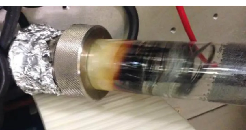
3.2 Picture of SiGe Growth Tube . . . 32
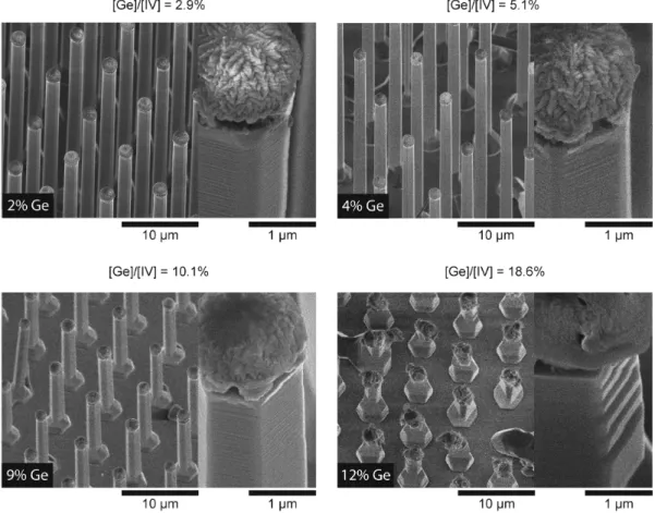
3.3 SEM image of SiGe wires of various compositions . . . 35
3.4 SEM image of SiGe wires grown to different lengths . . . 36
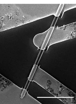
3.5 SEM image of four point contacts on a single SiGe wire . . . 38
3.6 Schematic of the photoconductivity measurement . . . 39
3.7 Results from photoconductivity measurements of single Si and SiGe wires . . . 39
4.1 Limiting efficiency of a 3µm thick device . . . 44
4.2 Limiting efficiency of a silicon solar cells with different thickness and SRV . . . 45
4.3 Optimal thickness for light trapping beyond the 4n2 limit . . . 46
4.4 SEM images of cryo-DRIE etched wires . . . 47
4.5 Lifetimes of planar DRIE etched wafers following damage removal . . . 48
4.6 Absorption measurements of etched wires on substrate . . . 50
4.7 Absorption measurements of peeled off etched wires . . . 51
5.1 Simulated band structures of GaP/Si heterojunctions . . . 56
5.2 Simulated efficiency of GaP/Si heterojunctions varying band alignment and defect con- centration . . . 57
5.3 Simulated band structures of GaP/Si heterojunctions . . . 58
5.4 Simulated efficiency of GaP/Si heterojunctions varying band alignment and defect con- centration . . . 59
5.5 Schematic of GaP substrate removal process . . . 62
5.6 Hall contact deposition mask . . . 63
5.7 Photograph of GaP films following substrate removal with a crystalbond wax interlayer 64 5.8 Confocal microscopy measurement of macroscale textured GaP film . . . 65
5.9 SEM images of substrate removed GaP with SU8 interlayers . . . 66
5.10 Optical image of GaP bonded directly to glass . . . 67
5.11 Tauc plot of substrate removed GaP film . . . 69
5.12 Photoluminescence spectra of undoped and Mg doped GaP films . . . 71
5.13 Time resolved photoluminescence of GaP . . . 71
5.14 X-ray diffraction measurement of substrate removed GaP film . . . 73
5.15 Images depicting the surface quality of substrate removed GaP films . . . 74
5.16 Current-voltage characteristics of GaP/Si heterojunction device . . . 75
5.17 Spectral response of GaP/Si heterojunction device . . . 76
6.1 Band diagram of amorphous silicon heterojunction device . . . 79
6.2 Simulated light beam induced current experiment . . . 81
6.3 Current splitting device fabrication scheme . . . 82
6.4 Current splitting experiment schematic . . . 83
6.5 Current splitting experiment results with 5 nm and 10 nm i-a-Si . . . 83
6.6 Schematic and LBIC maps of transport near a defect experiment . . . 84
6.7 Linescans of defects showing effective cross section width . . . 85
6.8 LBIC Map and Linescans around a defect . . . 86
6.9 Results . . . 86
A.1 Samples for a-Si thickness and conductivity measurements . . . 99
A.2 DC conductivity of n+ doped amorphous silicon . . . 100
A.3 Current-voltage and spectral response of simple heterojunction device . . . 101 A.4 Optical Constants of Oxides Deposited in PL5 . . . 102 B.1 Transient simulation output . . . 104
List of Tables
4.1 Parameters used for limiting efficiency calculations . . . 43
4.2 Lifetimes of DRIE etched wires . . . 50
5.1 Gallium Phosphide Hall Effect Measurements . . . 68
6.1 Results from Current Splitting Simulation . . . 80
A.1 Oxide/Suboxide Depositions from PL5 . . . 101
List of Publications
Portions of this thesis have been drawn from the following publications:
• H. Emmer and H. A. Atwater, “Measurement of silicon surface inversion induced by buffered hydrofluoric acid,”In Preperation, 2015.
• D. B. Turner-Evans, H. Emmer, C. T. Chen, and H. A. Atwater, “Flexible, transparent contacts for inorganic nanos- tructures and thin films,”Advanced Materials, vol. 25, no. 29, pp. 4018–4022, 2013. DOI:10.1002/adma.201300927 Contributed to wire growth and processing efforts, supported measurements
• C. T. Chen*, H. S. Emmer*, S. Aloni, D. B. Turner-Evans, and H. A. Atwater, “Cu-catalyzed vapor-liquid-solid growth of sige microwire arrays with chlorosilane and chlorogermane precursors,”Crystal Growth & Design, vol. 15, no. 8, pp. 3684–3689, 2015. DOI:10.1021/acs.cgd.5b00097 *equally contributing authors.
• D. B. Turner-Evans, C. T. Chen, H. Emmer, W. E. McMahon, and H. A. Atwater, “Optoelectronic analysis of multijunction wire array solar cells,”Journal of Applied Physics, vol. 114, no. 1, pp. –, 2013. DOI:10.1063/1.4812397 Supported device design and simulation efforts
• C. T. Chen, D. B. Turner-Evans, H. Emmer, S. Aloni, H. Atwater,et al., “Design and growth of iii-v on si microwire array tandem solar cells,” inPhotovoltaic Specialists Conference (PVSC), 2013 IEEE 39th, pp. 3397–3401, IEEE, 2013. DOI:10.1109/PVSC.2013.6745178
Contributed to silicon wire growth and processing efforts
• H. Emmer, C. T. Chen, R. Saive, D. Friedrich, Y. Horie, A. Arbabi, A. Faraon, and H. A. Atwater, “Fabrication of free standing crystalline gallium phosphide thin films,”In Preperation, 2015.
Chapter 6 draws heavily from:
• 2013 IEEE. Reprinted, with permission, from H. Emmer, M. Deceglie, Z. Holman, A. Descoeudres, S. De Wolf,c C. Ballif, and H. Atwater, “Experimental measurement of lateral transport in the inversion layer of silicon hetero- junction solar cells,” inPhotovoltaic Specialists Conference (PVSC), 2013 IEEE 39th, pp. 1229–1231, June 2013.
DOI:10.1109/PVSC.2013.6744362
• 2014 IEEE. Reprinted, with permission, from M. G. Deceglie, H. S. Emmer, Z. C. Holman, A. Descoeudres,c S. De Wolf, C. Ballif, H. Atwater,et al., “Scanning laser-beam-induced current measurements of lateral transport near-junction defects in silicon heterojunction solar cells,”Photovoltaics, IEEE Journal of, vol. 4, no. 1, pp. 154–
159, 2014. DOI:10.1109/JPHOTOV.2013.2289353
Contributed to experimental design, test device design and fabrication, measurement and analysis
Chapter 1
Introduction
1.1 Introduction
Photovoltaics hardly need any introduction today. This technology has successfully made its way from a laboratory curiosity, to a niche product, and finally to an important, mainstream electricity generation source. In the five year period of 2009-2014, total worldwide installed solar capacity has doubled three times from 22 GWp (Gigawatts of peak power output) to 177 GWp. As of 2014, photovoltaics provide 1% of the total electricity produced worldwide[1] and rapid growth is expected to continue.
This rapid growth is driven by a similarly rapid drop in prices. In 2010, the United States Department of Energy set a then-lofty goal of reaching total system installed costs of $1/Wp by 2020; this goal has likely already been met, five years early, in utility-scale installations [2]. Grid parity, as defined by the levelized cost of energy (LCOE) produced by a photovoltaic system equaling the cost of current retail electricity rates, has been surpassed in regions of 30 countries worldwide [2]. The passing of this critical threshold will fuel the continuation of rapid solar industry growth in the coming years.
The overarching goal of research efforts in the field of photovoltaics is continuing the reduction of total system costs, which enables the continued growth in the deployed photovoltaic capacity worldwide. This thesis explores technologies that hold potential to reduce the cost of silicon based photovoltaic systems by reducing the quantity of silicon material used and improving device effi- ciency. Improvements in efficiency have the potential to reduce total system costs by reducing the balance of system costs. As shown in figure 1.1, the module only makes up a small part of the cost of a residential photovoltaic installation. Many of the other (balance of system) costs, both hard costs like racking and wiring and soft costs like logistics, scale inversely with efficiency. Put simply, if the efficiency of a module increases by 10%, you are able to get 10% more power out of a system with the same amount of racking, labor, and warehouse space. Improvements in materials and device design and processing can directly reduce the module costs and improvements in device efficiency
Module InverterStructure
Electrical BOS (wiring, etc) Labor
DEPI
Supply Chain, Taxes, Logistics Customer2Acquisition
Overhead2and2Margin G4y00
G3y00
G2y00
G1y00
G0y00
Data2Source:2GTM2Research2Global2PV2BOS2 Landscape
20142UySy2Residential2PV2Average2Balance2of2Systems2 Costsy2Bolded2Costs2Scale2With2Efficiencyy
Figure 1.1: Breakdown of balance of systems costs in average 2014 United States residential PV installations. Bolded categories are expected to scale with efficiency.
can drive down the total cost of an installed photovoltaic system by reducing the balance of system costs.
1.2 Photovoltaic Device Operation and Performance
Total power conversion efficiency is the most important parameter in comparing the performance of photovoltaic devices in the majority of applications. We can break the efficiency down into three components:
η= VOCJSCF F Pin
Where VOC is the voltage at open circuit,JSC is the current density at short circuit, and F F is the fill factor, defined by the fraction or percentage ofVOCJSC that can be extracted from a cell at the maximum power point. This is shown visually in figure 1.2: The fill factor is the ratio of the area of the dark shaded rectangle to the light shaded rectangle.
1.2.1 Open Circuit Voltage
The fundamental operation of a photovoltaic device requires two basic steps. First, a photon must be absorbed by the material, causing the generation of an electron-hole pair. Second, the electron
VOC
-50 -40 -30 -20 -10 0 10 20 30 40 50
0 0.2 0.4 0.6 0.8
Curr ent Density (mA/cm
2)
Voltage (Volts)
Current-Voltage Characteristics of an Idealized High Performance
Silicon Device
JSC
Figure 1.2: Current-voltage characteristics of an idealized high performance silicon solar cell. Short circuit current density and open circuit voltage are labeled at the axis intercepts and the maximum power point is marked with an×.
and hole must be collected outside of the device at different energies. This is most often achieved using a semiconductor material and some form of a p-n junction. The p and n type regions can support different quasi-Fermi levels, or chemical potentials, fulfilling the second requirement. Like a Fermi level, the quasi-Fermi level describes a population distribution, in this case the population of minority carriers in each region. Therefore, the chemical potential difference, or voltage, established in a device is a function of the minority carrier population excited in the semiconductor material.
It is not, as commonly thought, a result of the built in potential of a p-n junction [3]. The open circuit voltage can be given as:
VOC= kT q ln
(NA+ ∆n)∆n n2i
where ∆nis the excess minority carrier concentration, or the injection level. The injection level can then be related to device parameters by:
∆n= Φ Wτef f
where Φ is the absorbed solar flux,W is the thickness of the device, andτef f is the effective minority carrier lifetime.
Thus, in order to increase the minority carrier density and the voltage of a device, there are three possible strategies. First, Φ could be increased. This is the strategy taken in concentrating photovoltaic modules, and indeed the voltages and therefore efficiencies under concentration are higher than under one sun. The second option is to reduce the thickness of the absorbing material.
The final parameter, the lifetime, is a measure of the overall material and surface interface quality.
1.2.2 Short Circuit Current
The short circuit current is a measure of how much light is converted to electron hole pairs and subsequently extracted from the device. In a high quality device, the vast majority of the generated electron hole pairs can be collected. Therefore, improvements to the short circuit current require an increase in the amount of incident light absorbed. Incident light can be lost to either reflection or incomplete absorption — light that enters and exits the material without being absorbed. There is a tradeoff between improvements inVOC andJSC that can be achieved by thinning the device. A high efficiency photovoltaic will incorporate light trapping which allows thin materials, which have higher voltages, to effectively absorb light and have high current as well.
1.2.3 Fill Factor
As defined earlier, the fill factor measures the squareness of the current-voltage characteristic. The fill factor is a function ofVOC, but the parameters that effect it the most are the series and shunt resistances, RS and RSH. These are generally considered engineering issues, somewhat removed from the design of the device. However, when considering new device geometries, it is important to consider, for example, the influence of base doping or transparent conductive oxide conductivity on RS.
1.3 Past, Present, and Future
For many years, the majority of solar cells sold were fabricated using a simple and cost effective design, consisting of a multi- or mono-crystalline p-type wafer with an aluminum back surface field/rear contact, a diffused phosphorous emitter, silicon nitride front passivation/antireflective coating, and silver screen printed front contacts. While there were many advances in device designs and record cells throughout the 1980s [4], few of these made any impact on industrially realizable designs. Industrial innovation yielded better and cheaper wafers, but the basic design remained unchanged for the majority of devices [5].
This trend of inexpensive, simple devices dominating the market is likely beginning to shift.
Several high efficiency device designs which were once considered exotic and expensive are currently on the market, and signs point to higher efficiency devices becoming more common in the future.
For example, Sunpower, which manufactures devices based on the high efficiency interdigitated back contact design, is currently one of very few profitable device manufacturers based in the United States. Sanyo/Panasonic has manufactured the HIT silicon heterojunction device for years, and SolarCity/Silevo is currently in the process of building the largest solar cell fab in the United States based on this high efficiency technology. Recently, researchers have developed a version of the passivated emitter, rear locally diffused (PERL) cell, which held the record for silicon device efficiency until recently, using only inexpensive process steps, achieving a 19.4% efficiency [6] industrially relevant device. It seems likely that this design will become widespread in the coming years.
The ultimate goal of photovoltaics research is to develop a low cost, deployable technology. As the photovoltaic industry continues to scale up, there will be significant investment in developing tools and techniques to continue reducing the cost of processes which may currently be expensive.
While original critics of Sunpower may have thought that patterning the interdigitated contacts would be too expensive, or the high quality wafers required for these devices would cost too much, the enabling process technologies have improved and proved to be commercially viable. Even atomic layer deposition [7] and ion implantation [8], both once widely thought to be cost prohibitive in solar applications, have recently received significant attention and will likely be viable in the near future.
Therefore, it is important to continue to research high efficiency devices, separate from the ability to make a commercially viable process today.
The work in this thesis explores the limits of high efficiency devices from two different, but related, angles. First, we examine the potential of microwires for use in extremely thin high efficiency devices.
Next, we explore the properties of the gallium phosphide/silicon and amorphous silicon/crystalline silicon heterojunction systems. As explored further, the latter is an enabling technology for the former. I believe that in the future, photovoltaics will be both high efficiency and low cost, and extremely thin heterojunction devices are likely candidates to achieve this.
Chapter 2
Advances in Silicon Microwire Photovoltaics
2.1 Introduction
The wire array photovoltaics project began several years before my arrival in the Atwater group, and some great achievements were made by the dozen or so students, post-docs, and professors working on this project. Notably, growth of high fidelity pattered wire arrays was achieved with a variety of catalyst materials [9] and over large area substrates [10]. Wire arrays were shown to absorb as much light as conventional wafer-based modules using only a small fraction of the material [11]. Large area devices achieved efficiencies of 9% [12], while single wire devices showed potential for efficiencies up to 17% [13]. Following these successes, a start-up company was spun out of our labs with the goal of bringing this technology to market.
The original motivation for the wire array photovoltaic project was to create a waferless silicon photovoltaic device. The patterning and growth processes were developed such that the silicon wafer which was used as the growth substrate would become a reusable piece of capital, rather than a consumable part of the photovoltaic module. A potentially scalable process to utilize this technology is:
1. A new silicon wafer with a thermal oxide is patterned by photolithography or imprint lithog- raphy
2. Copper catalyst particles are deposited in holes in the oxide by electrodeposition
3. Wires are grown by a vapor liquid solid chemical-vapor-deposition process from the copper catalyst particles, with p-n junction formed in situ
4. The wires are cleaned and sidewalls passivated
5. A flexible polymer is used to fill the spaces between the wires
< Ln
1/α 1/α, Ln
Radial Junction Axial Junction
Figure 2.1: Schematic of radial and axial junction devices. The axial junction geometry minimizes junction area and parasitic absorption, but requires longer minority carrier diffusion lengths, greater than the length of the wire rather than the radius, to extract carriers.
6. Wires are mechanically removed from the growth substrate contacted, and installed into a module
7. The substrate is reused many times, repeating from step #2
The wire devices previously developed had a junction in the radial direction, as shown schemat- ically in figure 2.1. This device geometry has the advantage of allowing the use of lower quality material by orthogonalizing the directions of light absorption and carrier collection [14]. In a planar solar cell, the minority carrier diffusion length (LD) must be much greater than the device thickness t, while the optical absorption length αmust be less than the thickness. This requirement ensures that light is fully absorbed in the cell and that carriers generated by light absorbed at the back of the cell can diffuse up to the junction and be extracted. The orthogonalization of these characteristic lengths means that we no longer require thatLD> t > α. Light is absorbed throughout the entire length of the wire device, while carriers can be extracted from the much smaller radius. Therefore, lower material quality as measured byLD, can be tolerated while still yielding good current collec- tion and decent efficiencies. However, ifLD is long, higher efficiencies can be achieved in an axial junction geometry, which minimizes the junction area and thus dark current. We explore the fea- sibility of improving device efficiency by transitioning to axial devices by evaluating the achievable minority carrier diffusion length.
During my tenure at Caltech, the price of a solar grade silicon wafer fell by an impressive 16%
annually, resulting in a wafer that costs less than one third of what it did when the silicon wire project began [15]. The focus on this project, and my own research focus, has therefore shifted from developing a low cost but moderate efficiency technology to realizing other potential advantages of these unique structures. Due to their high light absorption and high aspect ratio, micron-scale wires
are uniquely positioned for use in very high efficiency (>25%) photovoltaic devices. First, the high aspect ratio geometry of arrays of vertically oriented wires allows the potential to grow out defects in the horizontal direction and allow high quality, defect-free growth in the vertical direction [16].
Thus, vertically oriented wires could act as an ideal substrate for growth of tandem photovoltaics.
To this end, we investigated the growth of silicon-germanium alloy wires, which is presented in Chapter 3. Second, these wires, which have radii on the order of the wavelength of light, were found to absorb light very strongly — in some cases even exceeding the traditional 4n2 geometrical light trapping limit. This allows for the use of less material, and consequentially operation at higher injection levels and voltages. Progress towards devices based on this goal is presented in Chapter 4.
Prior to shifting focus away from VLS grown silicon wires, the broad goals of the silicon wire project were to continue on the path towards developing a commercially viable technology, which involved improving device efficiency and simplifying and improving the reproducibility of our growth process. Progress towards this goal included developing an in situ junction formation process which both provided a simple process and a means for measuring material quality, and investigation of our wire growth process at different temperature regimes.
2.2 In Situ Phosphorus Doping
Previously, only p-type doping was performed in situ by flowing boron trichloride (BCl3) during growth. The original decision to grow p-type silicon wires and form junctions by diffusion doping n-type emitters was likely due to safety concerns; BCl3 gas and solid phosphorus diffusion sources are significantly less hazardous than phosphine (PH3) gas. Solar cells with p-type bases also provide a number of other potential advantages. First, electrons have higher mobilities than holes, and therefore the minority carrier diffusion length is longer in p-type material given equal electron and hole lifetimes. Second, while it does not result in the highest efficiency device, it is a simple process to form both a back contact and back surface field in p-type silicon by firing aluminum onto the rear. Finally, it is well known that phosphorous diffusion acts to getter metal impurities, including copper and iron which are likely present in our VLS wire material, from silicon [17]. The potential disadvantage of p-type base material, and one of the major forces driving the conventional photovoltaic industry towards n-type wafers, is the formation of boron-oxygen dimers, which form a deep level trap [18]. However, this is more relevant in very high quality material; residual copper and other metal impurities or surface effects will dominate the lifetime of wires, rather than B-O complexes.
Despite the noted advantages of p-type base material, it was desirable to add the capability to grow n-type material as well. The original goal was to use n-type silicon as photoanodes in a photoelectrochemical water splitting device [19]. Upon my arrival to Caltech, a bottle of dilute
0 0.01 0.02 0.03 0.04 0.05 0.06 0.07 0.08
0 0.5 1
Resistivity (Ω-cm)
Phosphine Flow (sccm)
0 1E+18 2E+18 3E+18 4E+18
0 0.5 1
Doping Density (cm-3)
Phosphine Flow (sccm)
Figure 2.2: Phosphine doping calibration. Resistivity was measured with four point measurements, and doping density inferred from resistivity using standard mobility values [20].
phosphine (PH3, 500 ppm in H2) had recently been added to the wire growth CVD reactor located in the Noyes lab. This added capability opened up the door to the growth of in situ junctions, as described in the next section.
Initial growths were performed at low flow rates, and the effects of doping characterized by measuring resistivity using four point contacts. The measured resistivites and the corresponding expected doping concentrations are shown in figure 2.2. Anecdotally, the growth rate and fidelity seemed to drop slightly compared to undoped growths when using PH3 doping, but at the time of the initial characterization, the growths were not reproducible enough to well quantify these effects.
This would be in contrast to the increase in growth rate and fidelity observed in growths using BCl3
doping. Despite these effects, it was possible to grow high quality arrays of n-doped wires with in situ phosphine doping.
As observed more directly and discussed further in the next section, it was observed that the phosphorus created a heavily doped core by diffusing in from the sidewalls during growth. The resistivity measured following a surface etch was significantly higher than before. This contrasts with the p-type growths, in which the measured resistivity does not significantly change after the cleaning and surface etch process.
2.3 In Situ Junction Formation
The state of the art junction formation process for microwire array solar cell fabrication in our group was a fairly complicated process which involved several steps. First, the wire array is oxidized to
create a diffusion masking oxide. A polymer infill is then used to define the junction height, and the oxide above the polymer is etched away, leaving a “boot” at the bottom which prevented the n+ emitter from shorting to the p+ substrate/back surface field region. The array is then cleaned before a diffusion doping step is performed to create a p-n junction. A schematic of this process and more details are available elsewhere [12].
In contrast, an in situ junction formation process offers many advantages over the diffusion junction formation process. The first advantage to this process is simplicity and reproducibility.
Achieving a reproducible polymer infill height has consistently been one of the more challenging steps in the device fabrication process. When considering scaling up production, an in situ junction formation is not only easier to perform reproducibly, but also eliminates two high temperature or vacuum deposition steps, allowing for a lower device cost.
Another advantage, and the original motivation for developing this process, is that junction formation does not require a high temperature step after growth. These devices can therefore be used to probe the material quality of the wire as it is grown, and separate out any influence of other processing steps which could add (or remove) impurities. Another possible option that fulfills these requirements would mimic the previously used radial junction process, but replace the thermal oxidation with a low temperature plasma enhanced chemical vapor deposition (PECVD) or physical vapor deposition oxide deposition, and replace the diffusion doping step with a PECVD amorphous silicon (a-Si) deposition. However, the capability to deposit n+ doped a-Si was not yet available in our labs at this time; additionally, this process would still require the poorly controlled polymer infill step.
Finally, the end result of the in situ junction formation process will be an axial junction device.
As described previously, the axial junction has the potential to achieve higher efficiencies than radial junction devices, but will require high material quality.
2.3.1 Growth of Wires with In Situ Junctions
The most successful process for growing in situ junctions turned out to be the simplest. The growth process began using the same techniques to pattern and grow p-doped wire arrays, but three quarters of the way through the growth, the dopant gas was switched to phosphine. The maximum phosphine flow rate was used, and it is expected that this gave doping concentrations in the 1019cm−3range, based on measurements at lower flow rates.
One potential concern was the abruptness of the junction. The growth rate of the wires varied from about 5-10 microns per minute. It is estimated that the residence time of the reactor is approximately one minute, resulting in a worst case junction that is graded along a 10 micron length. An attempt was made to grow wires with a more abrupt junction by pausing the growth and purging the base dopant before introducing the emitter dopant. The SiCl4 and BCl3flows were
stopped, leaving the H2 carrier gas purging the system, for two minutes or more minutes. This corresponds to approximately two times the gas residence time in the reactor. This resulted in a defective region visible in figure 2.3. Without further investigation, it seems as though the defective growth begins as the precursor concentration in the reactor and the catalyst particle decays, and a second, larger, defect occurs as growth resumes. All samples in which growth was paused and resumed had very high series resistance and poor diode ideality. The samples without a pause had quite good ideality (<2) and reasonable series resistance. Light beam induced current measurements on unpassivated wires, as shown in the following section, resulted in a small spot, indicating that the junction is fairly abrupt. This is not surprising; it is expected that the flow of gasses in the reactor growth tube is reasonably laminar, and the diffusion through the gas mix would be a much smaller effect than mixing within the growth tube. Further improvement would require both better measurements of junction profile, and design of a reactor which minimizes dead time and gas mixing.
It is also important to note that good devices were only obtained in the first growth in which phosphorous was introduced in the tube. Subsequent growths resulted in single wire devices which gave ohmic behavior, implying that the phosphorous from the tube sidewalls was mobile enough to cause the base to become n-type. Thus, the usual growth process involved doing two or three intrinsic or p-doped growths to condition a new tube, and once high fidelity, stable growth is realized, performing a single in situ junction forming growth. In a scaled process, it may be possible to remove the doped surface growth by etching in potassium hydroxide; this was not attempted, as the small tubes used in that reactor are inexpensive enough to simply replace.
2.3.2 Measurements of In Situ Junctions in Single Wires
The main techniques used to characterize the in situ grown wires were current-voltage (IV) and light beam induced current (LBIC) measurements on single wires. Single wires were contacted according to the following process:
1. Wires are cleaned on-substrate. Cleaning process varied, as described below, but generally consisted of RCA cleans to remove the copper catalyst and surface contamination.
2. A razor blade was used to mechanically scrape wires off the growth substrate and disperse wires in isopropanol.
3. The wires dispersed in isopropanol are spun onto a low pressure CVD silicon nitride coated silicon wafer, for 30 seconds at 300 RPM, 30 second at 600 RPM, and 1 minute at 1200 RPM.
4. Microchem LOR10a is spun on the substrate at 1500 RPM for 30 seconds to aid in liftoff after contacting the wires with thick metal.
Emitter
Base
Defective Region
Figure 2.3: Attempt at in situ junction growth with a pause to purge the base dopant. Inset (upper left) shows the wire at near-normal incidence, with the same scale, showing higher contrast in the defective region.
5. Individual wires are patterned using Shipley S1813 photoresist and a dark field mask to allow multiple exposures on each chip.
6. Contacts are formed with about 1µm of metal. Both aluminum capped with silver and gold capped with titanium were used successfully. The aluminum contacts require an anneal at 200-400◦C
Current-voltage measurements are presented in this section using a current density, normalized to an approximate cross sectional wire area. Note that for wires, this is different from the total junction area, as relevant in dark current measurements, and potentially different from the light absorption cross section. This is because these wires, which have dimensions on the order of the wavelength of light, may absorb light beyond their physical extents. While for these reasons it is difficult to extract actual large area device parameters from individual wire measurements, it is straightforward and valuable to compare single wires from different samples using these techniques.
Light beam induced current measurements were performed with a Zeiss LSM 710 scanning con- focal microscope. The wire current output is fed into a home built transimpedance amplifier with a gain of 100 kΩ and into the microscope through a connector spliced into the photomultiplier tube input. The microscope software is then able to form an image from the photocurrent signal. The scale of the current intensity can be measured using a calibrated photodiode, and the quantum effi- ciency can be extracted from the measurement. However, current data is presented here in arbitrary
units, useful as a comparison between different areas of the same sample. Ideally, the intensity of the photocurrent signal in the base, moving away from the junction, can be fit to an exponential which corresponds to the diffusion lengthLD in the wire base. However, as discussed in the following sec- tions, generation of current in the base, even combined with an exponential decay, is often indicative of the presence of a radial carrier separation and collection path, rather than a long diffusion length into the base.
Following growth, the samples were cleaned to remove the copper catalyst, and single wire contacts were made. Immediately following growth, a thin n-type region was present throughout the length of the wire, forming a lightly doped emitter shell around the base core. Evidence of this is shown in figure 2.4, in both the IV curve and light beam induced current (LBIC) image. Current was collected throughout the length of the wire, with no surface passivation applied. Additionally, the low open circuit voltage of approximately 300 mV and high series resistance both result from the thin, high sheet resistance emitter shell that formed during growth. The high resistance caused an extremely low fill factor of 27%, and the resulting single wire device total power conversion efficiency was approximately 2%.
A potassium hydroxide etch was used to remove the n-doped region from the surface. Considering the growth time and temperature,√
Dtfor phosphorous diffusion into silicon is about 20 nm, so the target etch depth was approximately 30 nm. The samples were etched in 40% KOH for 1 minute and 30 seconds at room temperature. After this, a second RCA 2 clean was used to remove any remaining metal ions. Resulting device IV curves and LBIC images are shown in figure 2.5, and reveal that the radial junction was successfully removed. Once the surface etch is performed, reasonable diode characteristics are revealed, but recombination in the base region prevents electrons from reaching the axial junction for collection. As a result, the total photocurrent is very low, and only the region right around the junction lights up in LBIC measurements.
Silicon nitride (SiNx) and amorphous silicon (a-Si) were used as surface passivation treatments, and these samples were also characterized with I-V curves and LBIC microscopy. Results from a champion SiNxpassivated device are shown in figure 2.6. While full current collection was achieved in the base, the open circuit voltages were lower than expected for a high performing axial junction device. The champion device had a Voc of 475 mV, while the average voltage obtained from single wire devices was 406 mV. The likely cause of this is a high density of fixed positive charges at the Si/SiNx interface well known to be present in PECVD deposited films [21]. These interface fixed charges cause inversion at the outer surface of the SiNx coated base region. This inverted region induces a radial junction, and thus provides a path for electrons to reach the n-doped silicon emitter as majority carriers.
The a-Si, on the other hand, passivates the surface but the carrier collection length in the axial region remains extremely low, likely limited by the lifetime, and consequently diffusion length, in the
-20 -15 -10 -5 0 5 10
0 0.2 0.4 0.6 0.8
Current Density (mA/cm2)
Voltage (V)
Typical As Grown In Situ Junction Light and Dark I-V
Dark Light
Figure 2.4: (left) Current-voltage characteristic of a typical in situ junction device, following cleaning to remove the catalyst particle but without a surface etch. VOC= 291 mV andJSC = 11.20 mA/cm2. (right) Light beam induced current measurements reveal current collection from the entire base region, with moderate decay.
-10 0 10 20 30 40
0 0.2 0.4 0.6 0.8
Current Density (mA/cm2)
Voltage
In Situ Junction After Surface Etch Light and Dark I-V
Dark Light
Figure 2.5: Current-voltage characteristic of the champion situ junction device following a KOH surface etch. VOC = 336 mV and JSC = 0.40 mA/cm2. All other samples exhibited unmeasur- ably small photoresponse. Light beam induced current measurements (not pictured) reveal current collection from a very small region, on the order of one micron, near the junction.
-20 -10 0 10 20 30 40
0 0.2 0.4 0.6 0.8
Current Density (mA/cm2)
Voltage
In Situ Junction With SiNx Passivation Light and Dark I-V
Dark Light
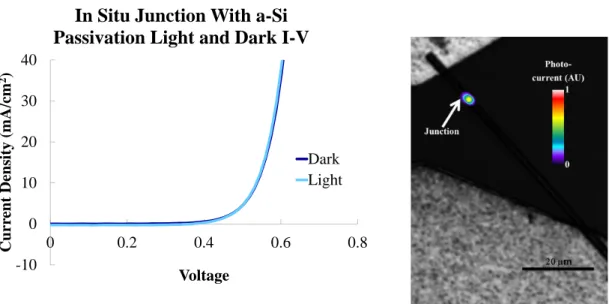
Figure 2.6: Current-voltage characteristic (left) and light beam induced current measurement (right) of a champion in situ junction device, following surface clean and etch and SiNxpassivation. Current is normalized to the exposed base region area. VOC = 475 mV andJSC = 17.4 mA/cm2. Light beam induced current measurements reveal a characteristic collection length of 9.3µm, with excellent fit to a single exponential decay (R2 = 0.998).
bulk. Current-voltage and LBIC measurements of a typical sample are shown in figure 2.7. The open circuit photovoltages are consistently measureable, a significant improvement over the unpassivated devices. The champion device exhibited a photovoltage of 406 mV.
Current-voltage characteristics measured in the dark provide additional evidence that the a-Si effectively passivates the sidewall surfaces. As shown in figure 2.8, the dark current is suppressed by a-Si passivation, and actually increases in the SiNx coated sample compared to the bare one.
The sensitivity of this measurement and the ability to fit dark current parameters J01 and J02 was hampered by the small size of the device and extremely small absolute currents (picoamperes) at low bias voltages. Additionally, the a-Si passivation used here caused an increase in series resistance, as evidenced by the dark current curve becoming less linear at lower voltages. The deposition could likely be optimized, resulting in a thinner passivating film which would not provide the same series resistance, and absorb less light. Regardless of the shortcomings of the measurement, it is clear that the a-Si sample exhibited significantly reduced dark current, evidence of effective surface passivation.
Thus, surface passivation alone is not sufficient to increase the current collection length in the base.
This picture of current collection increasing due to surface inversion helps to explain the results of previous work on diffusion doped wire devices with radial and axial regions [13]. In these devices, silicon nitride passivation resulted in an increase in current extracted from the axial junction region of the wire, but resulted in a lower overall voltage than amorphous silicon passivated samples. An increase in current due to passivating a recombination active surface should be accompanied by
-10 0 10 20 30 40
0 0.2 0.4 0.6 0.8
Current Density (mA/cm2)
Voltage
In Situ Junction With a-Si Passivation Light and Dark I-V
Dark Light
Figure 2.7: Current-voltage characteristic (left) and light beam induced current measurement (right) of a in situ junction device, following surface clean and etch and amorphous silicon passivation.
Current is normalized to the exposed base region area. VOC= 370 mV andJSC = 0.3 mA/cm2. Light beam induced current measurements reveal collection from only the region within approximately 1µm from the junction.
0.2 2 20 200 2000
0 0.2 0.4 0.6 0.8
Current Density (mA/cm2)
Voltage
In Situ Junction With and Without Passivation Dark I-V
SiNx No Passivation a-Si
Figure 2.8: Dark I-V curves of in situ junctions. Dark currents are normalized to the axial junction area, the wire cross section. Amorphous silicon provides effective passivation, resulting in a shift in the dark current curve. The small increase in dark current in the SiNx coated sample could result from the increased junction area induced by fixed charges in the SiNx layer, as described.
an increase in voltage; the best explanation for the trend observed is that the improved current collection was caused by surface inversion, rather than surface passivation, and resulted in decreased voltage due to the increase in junction area in defective material.
2.4 Material Quality Measurements
One key measure of material quality is the overall effective lifetime,τef f of photogenerated minority carriers. The effective lifetime is given by τ1
ef f = τ1
bulk+τ 1
surf ace+· · ·. In silicon, the most important
contribution toτbulkis Shockley-Reed-Hall recombination, the recombination of free carriers through defect states within the band gap.
As discussed earlier, the original goal of developing an in situ junction formation process was to measure, and eventually improve, the electronic quality of as-grown silicon wires.
2.4.1 Light Beam Induced Current with Chemical Passivation
In order to assess the bulk material quality, the influence of the surface must be eliminated. While it is not a practical method for a complete solid state device, excellent surface passivation can be achieved by submerging the sample in a variety of different solutions. These include:
1. Strong acidic solutions, with the best performance from hydrofluoric acid [22]
2. Iodine in alcohol (methanol or ethanol) [23]
3. Quinhydrone in alcohol (methanol or ethanol) [24]
4. Strong basic solutions, such as 40% sodium hydroxide[25]
We attempted to apply this same principle to light beam induced current diffusion length mea- surements by submerging the sample in solution during measurement. The first method, passivation in acidic solutions, was deemed most appropriate. Basic solutions etch silicon, and the wires would be fully consumed after exposure to bases. Attempts were made to use the alcohol based solu- tions, but due to their high volatility, it was difficult to take measurements prior to the solution evaporating, even when care was taken to cover the sample. It may be possible to fully seal the sample within an alcohol containing environment to take this measurement, but instead acids were used, as in previous work in our group [13]. First, single wires were patterned and contacted as described previously. Next, a second photolithography step was used, leaving a protective coating of photoresist over the contacts and a well which allowed the acid to come in contact with the wire.
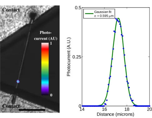
Measurements were first taken with a drop of 18 MΩ deionized water as a control. The results are shown in figure 2.9; this measurement puts an upper limit on the LBIC spot size as a Gaussian with σ= 0.595µm. In situ grown axial junction samples with different post growth processing methods
Photo- current (AU)
0 1
14 16 18 20
0 0.25 0.5
Distance (microns)
Photocurrent (A.U.)
Gaussian fit σ = 0.595 µm
Contact
Contact
Figure 2.9: Control measurement of the sample shown in figure 2.10B, submerged in DI water.
Only the junction reveals current collection, indicating a sharp axial junction with extremely short diffusion length, as expected in the sample without surface passivation. A profile of the light beam induced current measurement (right) fits a Gaussian ofσ= 0.595µm with R2 = 0.996. This corre- sponds to an upper limit on the illumination spot size. Scale bar is 20 microns.
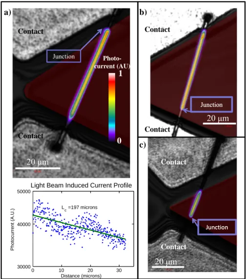
were measured with light beam induced current measurements using a buffered hydrofluoric acid (BHF, Buffer HF Improved, Transene) surface treatment. The results, as shown in figure 2.10, show current collection throughout the base of the wire on the samples which has a post-growth oxidation step. This data was initially interpreted as an improved diffusion length after post-growth oxidation.
However, upon further analysis, it became clear that as in the case of silicon nitride passivation, the hydrofluoric acid was causing the outer surface of the wire to become inverted and form an induced radial current collection path.
The most convincing piece of evidence in support of the hydrofluoric acid inverting the surface is the lack of diffusion towards recombination active surfaces. This can be seen clearly in samples which had a large gap between the contact and liquid passivation, as shown in figure 2.10 C. The unpassivated region between the contact and the well of BHF exhibits high surface recombination, and no current is extracted from this region, as evidenced by the dark LBIC measurement. If the remainder of the device was exhibiting good passivation and an axial junction, we would expect a decay in the LBIC profile in this device. This is because a carrier generated in the center of the active region of this device should have an equal probability of diffusing to either the recombination active area or the axial p-n junction. Assuming the lifetime of the carriers is long enough to result
20 μm
Junction Junction
Junction Junction
20 μm 20 μm
a) b)
c)
Junction Photo-
current (AU)
0 1
Contact Contact
Contact
Contact Contact
Contact
0 10 20 30
30000 40000 50000
Light Beam Induced Current Profile
Distance (microns)
Photocurrent (A.U.)
Lc=197 microns
Figure 2.10: Light beam induced current measurements in false color overlaid on optical images of wires with axial junctions submerged in buffered hydrofluoric acid (BHF). The photoresist well which cotains the HF is highlighted in red. Below sample A is a line scan of the photocurrent, showing little decay and a high apparent diffusion length. Sample B again clearly shows a long diffusion length in the base and short in the emitter, even when submerged in BHF. Sample C shows an extremely fast decay of photocurrent outside the well containing BHF, which strongly suggests that the BHF is inverting the surface inducing a radial junction.
in a diffusion length that is longer than the length of the wire, this situation can be modeled as a one-dimensional random walk. Carriers which reach the recombination active region will be lost, and the ones which reach the junction collected. For the ideal case with a long lifetime, the result will be a LBIC profile linearly decaying between a maximum at the junction and zero by the recombination active region. As the diffusion length reduces to the order of the length of the wire, the linear decay profile will be convoluted with an exponential decay with characteristic length of the diffusion length.
In order to achieve constant collection from all regions of the device, the entire base would need to have excellent passivation for minority carriers, including the region around the back contact.
Neither a linear nor exponential decay across the length of the wire was observed, as shown in figure 2.10. Instead, collection is relatively constant throughout the length of the wire, and rapidly decaying away from the region where the wire surface is no longer in contact with hydrofluoric acid.
This implies that the surface must be inverted, providing a second path for carrier separation and extraction in the radial direction.
2.4.2 Lifetime Measurements
2.4.2.1 Motivation
Lifetimes were measured directly in order to corroborate the diffusion length measurements. The two quantities are related by:
L=p Dτef f
whereD is the minority carrier diffusivity, related to the mobilityµby the Einstein relation:
D=µkBT q
The maximum attainable value for the electron diffusivityDe is approximately 36.5 cm2s−1, corre- sponding to an electron mobility µe of 1400 cm2V−1s−1. In order to obtain a diffusion length of 197µm, as extracted from the measurement in figure 2.10 A, at minimum, τef f would need to be greater than 10µs. This requirement becomes even stricter in doped or otherwise defective silicon material, where the mobility, and therefore diffusivity, is reduced. A realistic upper bound consider- ing the base doping of our silicon wire material of 1−5×1017cm−3is likely closer to 20µs, assuming µe= 700 cm2V−1s−1andDe= 18 cm2s−1. That is, in order for the measured light beam induced current decay to correspond to a diffusion length rather than surface inversion, the minority carrier lifetime in the wire must be longer than 20µs.
Nd:YAG
(1064 nm, 4‐6 ns pulse)
Gunn Diode Microwave Source
Finline Detector
Fast Amplifier
Oscilloscope Circulator
Figure 2.11: Schematic of microwave detected photoconductivity decay setup.
2.4.2.2 Measurement
Lifetime measurements on silicon wires were performed using a home built microwave detected photoconductivity tool. The illumination source is a Nd:YAG laser which provides a 30-240µJ, 3 mm diameter, 4 ns pulse. A schematic of the measurement apparatus is shown in figure 2.11.
Lifetimes of uncleaned, unpassivated vapor-liquid-solid grown wires as low as 20 ns were measured, proving the minimum measureable lifetime was quite low.
It is normally most informative to measure the lifetime at different, known minority carrier densities, but it is difficult to know the exact minority carrier density in this configuration. Some light will scatter or be absorbed in the centrifuge tube and liquid passivation. Also, while 1064 nm light is absorbed only weakly in silicon, and we can assume that the generation will be uniform in a wafer, these wires have the potential to form large clumps where the beam will be significantly attenuated, causing a distribution of injection levels inside the wires. Neglecting these attenuating effects, the maximum injection level excited by the 30-240 µJ pulse ranges from 5.4×10¹⁶ to 4.3×1017cm−3; we expect the actual excess carrier density of this measurement to be somewhat lower, but likely within an order of magnitude of these values.
One reason that it is important to know the injection level of the measurement is to get infor- mation about the recombination mechanism. An idealized plot of lifetime as a function of injection level for a silicon device is shown in figure 2.12 [26]. While the exact density is not known, the recombination mechanism can be predicted by considering the trend in lifetime as a function of laser intensity. All measurements on VLS wires showed either a flat or an increasing trend, characteristic
Figure 2.12: Typical curve of lifetime as a function of carrier injection level due to a combination of physical mechanisms: SRH, Auger, and emitter recombination. The increase in lifetime is caused by the transition to high level injection SRH statistics and the strong decrease at high injection levels is caused by Auger recombination. From [26].
of Shockley-Reed-Hall recombination, or the transition from low to high level injection, respectively.
Had the lifetime been limited by Auger recombination, the lifetime would decrease with increasing injection. This recombination regime likely corresponds to the injection levels most relevant to flat plate (non-concentrating) photovoltaic devices, and thus, the lifetime extracted can be considered a relevant lifetime governing device operation.
2.4.2.3 Results
The lifetime of undoped wires grown prior to and cleaned with the same process as the axial junction wires shown in figure 2.10 was measured. Intrinsic silicon has a larger change in conductivity under illumination than doped material, and therefore provides significantly more microwave photocon- ductivity decay signal, which is important to be able to measure microwires. The lifetimes measured are considered an upper bound for the devices made with doped material. Champion lifetimes, measured at a laser intensity of 60µJ per pulse, were 250 ns with BHF passivation and 430 ns under 6 M hydrochloric acid. There are several possible reasons for the higher lifetime provided by HCl passivation, including improved wetting of the wire surface (hydrofluoric acid renders the silicon sur- face hydrophobic), and the potential for hydrochloric acid to clean any remaining metal impurities from the wire surface. Still, the highest lifetimes measured were far below the 10-20 µs required to
obtain a diffusion length of 197µm. Assuming the same upper bound onDe of 18 cm2s−1 for the doped base, this corresponds to an upper bound on diffusion length of 27µm, significantly shorter than the measured collection length, again implying that the collection must be governed by radial collection through an inverted surface.
2.4.3 Summary and Discussion
In summary, these wires present many challenges in both measuring and achieving high material quality. While they present a unique opportunity to visually measure the collection length directly through light beam induced current measurements, great care must be taken to ensure that the surface is not inverted, and the measurement corresponds to the actual diffusion length. The best way to do this is to use a dielectric passivation with known fixed charge of opposite sign of the doping in the base region, such as silicon nitride for n-base devices or alumina for p-base devices.
Unfortunately, the arrival of our atomic layer deposition tool and achievement of good passivation with ALD alumina on silicon wafers coincided with a long period of downtime for the wire growth reactor. Additionally, lifetime measurements with acid passivation provide compelling evidence that the bulk material quality of the VLS grown wires is poor, and diffusion lengths will be short; these lifetime measurements may be a more reliable way to assess material quality in the future.
2.5 High and Low Temperature Growth
The vapor-liquid-solid growth process is a relatively complicated, with several steps which could be affected by temperature. Early work studying VLS growth of various semiconductor materials breaks the process down into four basic steps [27]:
1. transport of precursors in the gas phase to the liquid interface
2. chemical reactions at the liquid catalyst interface and subsequent intake of silicon into the liquid
3. transport of silicon through the liquid to the liquid/solid interface 4. crystallization of silicon from the supersaturated liquid at solid interface
It is fairly easy to rule out steps 1 and 3 as rate limiting steps by observing the effect of changing precursor concentration in the tube and the growth rates of different diameter wires, with different catalyst height. However, there is less convincing evidence for or against steps 2 and 4, and it is possible that both can play a role in determining the growth rate [28].
Aside from determining the rate of one or more activated steps of the growth process, temperature plays an important role in two additional steps. The first is the temperature required for liquid
![Figure 2.2: Phosphine doping calibration. Resistivity was measured with four point measurements, and doping density inferred from resistivity using standard mobility values [20].](https://thumb-ap.123doks.com/thumbv2/123dok/11844997.0/24.918.300.679.133.415/phosphine-calibration-resistivity-measured-measurements-inferred-resistivity-standard.webp)