250 C.2 SEM images of Si ICP-RIE etching with different gas flow and RF power. 253 C.3 Angled and top view SEM images of the Si etch used in the fabrication of a high-Q PC.
Acronyms
TE Transverse electric polarization, defined in this thesis as having electric field components predominantly in-plane and magnetic field components predominantly out-of-plane. TM Transverse magnetic polarization, which is defined in this thesis as having magnetic field components predominantly in-plane and electric field predominantly out-of-plane.
Preface
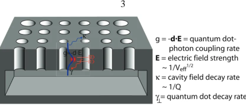
The centerpiece of the cleanroom will be an Oxford Instruments Plasma Technology (OIPT) inductively coupled plasma reactive ion etching (ICP-RIE) tool coupled with a plasma enhanced chemical vapor deposition (PECVD) tool. Simulations of the predicted behavior of these structures in the strong coupling regime of cavity QED are also considered.
List of Publications
Painter, Experimental demonstration of evanescent coupling with tapered optical fibers to photonic crystal waveguides, Electronics Letters, 39(11), p. Cho, Fabrication methods for a quantum cascade photonic crystal surface-emitting laser, Journal of Vacuum Science and Technology B, 21( 6), p.
Development of Ultrasmall Volume, High-Q Photonic Crystal Microcavities
Finally, Chapters 3 and 4 describe the experimental implementation of these designs within an InP-based multi-quantum well material and within silicon, respectively. The former chapter presents photoluminescence measurements of the InP-based devices, while the latter chapter uses an optical fiber tapered waveguide to passively probe the properties of the silicon resonators.
Semianalytic Methods for Studying Localized Modes Within
Two-Dimensional Photonic Crystals
Symmetry-based analysis
- Introduction
- Hexagonal lattice photonic crystals
- X-point
- J-point
- Conduction band donor modes
- Valence band acceptor modes
- Square lattice photonic crystals
- X-point
- M-point
- Conduction band donor modes
- Valence band acceptor modes
- Comparison with FDTD simulations
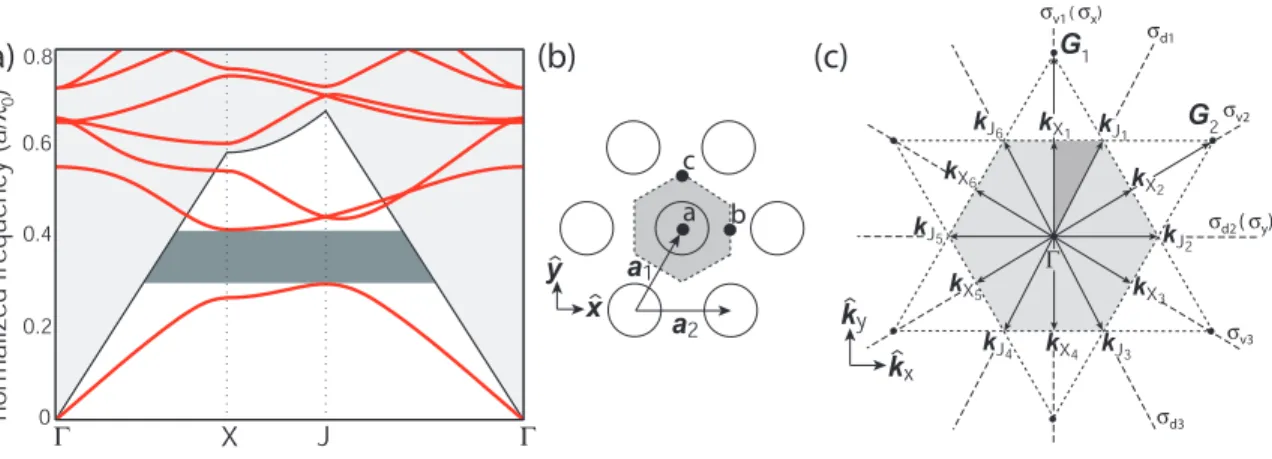
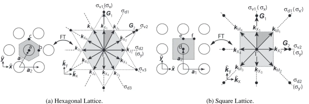
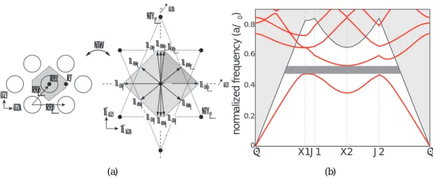
Inside the mirror plane of the plate, the magnetic field pattern for the (fundamental) TE-like eigenmodes of the unpatterned plate waveguide can be written as Hk⊥(r⊥) = ˆze−i(k⊥·r⊥), where k ⊥. For a hexagonal lattice, the valence band maximum occurs at point J (see figure). For a square lattice, the maximum of the valence band occurs at point M (Fig.
Wannier-like approach for describing localized modes in photonic crystalscrystals
- Introduction
- Wannier theorem for photons in periodic dielectric structures
- Envelope function calculation
- Donor modes at the X -point
- Acceptor modes at the J-point
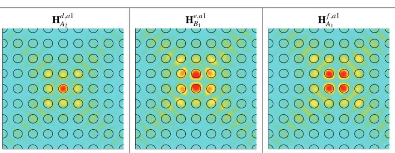
Assuming that the amplitude of the relatively large Fourier components Δη(r) associated with the mixing of states between the neighborhoods of different satellite points is much smaller than the amplitude of the small Fourier components that mix the states in the given neighborhood of the point, then we can consider the inter-ki mixing as a disturbance of envelopes functions arising from local mixing of k-space [104]. From equation (1.20), we have the form for the acceptor modes formed at the J-point of the hexagonal lattice. The FDTD plots of the calculated magnetic field patterns of these modes are given in Fig.
Introduction
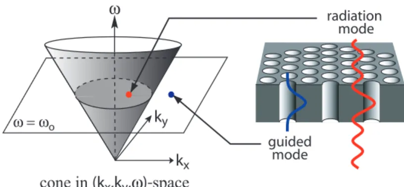
In Section 2.2 we describe a simple picture illustrating that the vertical radiation loss of the mode is characterized by the presence of momentum components within the light cone of the host slab (WG) waveguide cladding. In Section 2.5, we consider further improvements to the designs based on fitting the defect geometries in Fourier space, which minimizes the coupling of the dominant Fourier components of the mode with the radiating components. Results of FDTD simulations of these improved designs in a square lattice are presented and show that a modal factor Q approaching 105 can be achieved by careful consideration of the mode and error geometry in Fourier space.
Momentum space consideration of vertical radiation loss
Vertical radiation loss occurs when the magnitude of the in-plane pulse component, k⊥, is inadequate to support guidance. In particular, we look for structures that support resonant modes whose in-plane momentum components are primarily located outside the light cone of the cladding. These low-momentum components radiate and are the cause of the mode's relatively low effective vertical Q-factor (Q⊥≈1000).
Summary of the symmetry analysis of defect modes in hexagonal and square latticesand square lattices
- Hexagonal lattice
- Square lattice
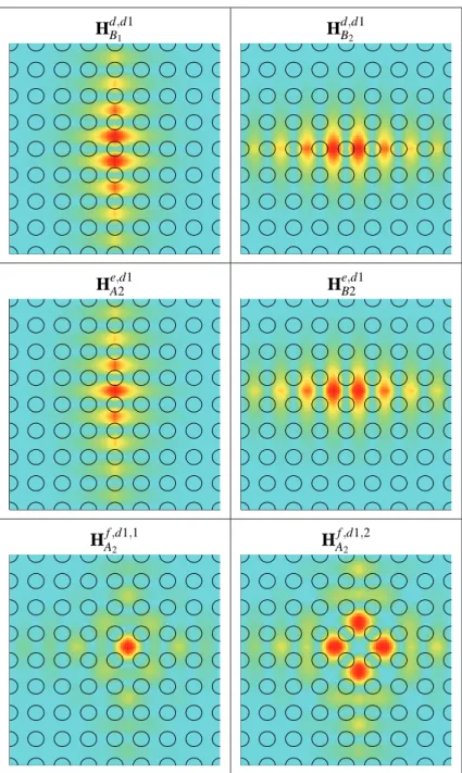
The course of the study is as follows: we use the results of this group theory-based analysis to determine the symmetry and dominant Fourier components for available donor- and acceptor-type modes formed at various high symmetry points within the PCs with hexagonal and square mesh. These tables provide the labeling scheme for the C6v and C2v modes, the dominant Fourier components of the modes, and their transform properties with respect to the available mirror planes (mirror plane properties are represented by their character values [92]). Decreasing the symmetry of the mode in C2v (through a modified defect at point a or recentralization at point b) results in modes with dominant Fourier components that are not orthogonal to the available mirror planes, or as in the case of Hb, the d1B1 mode, have incorrect spatial symmetry.
Initial FDTD simulation results
- Hexagonal lattice
- Square lattice
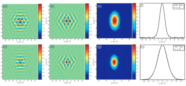
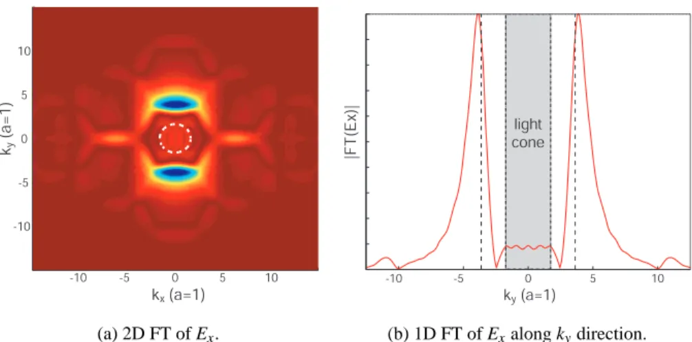
The defect is surrounded by a total of 8 periods of the hexagonal lattice in the ˆx direction and 12 periods in the ˆy direction. 2In our original papers [21, 23] we quoted modal volumes in terms of cubic wavelengths in air (λ3); this unit is important in terms of describing the physical volume of the field. The magnetic field amplitude and 2D spatial FTs (ExandEy) for the mode are given in Table 2.7.
Momentum space design of the defect geometry in a square lattice
Δη induces the changeδHd(r) in the defect mode, and this change is written as a superposition over the set of nearly (frequency) degenerate conducted and radiation modes of the PC sheet WG. As a result, it is desirable to minimize the Fourier components of the dielectric perturbation over an extended region around ky=±π/a. The FDTD simulations of the defect mode of this structure largely confirm the ideas described so far.
Defect modes in a compressed hexagonal lattice
- Preliminary analysis
- FDTD results
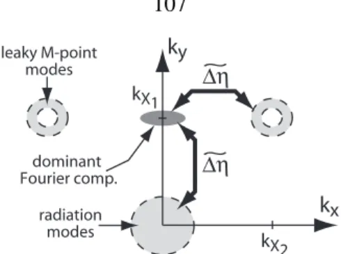
This is a reflection of the fact that the kXi are not mutually orthogonal (nor is the kJi). Consider the real and reciprocal space representations of the compressed hexagonal lattice as illustrated in fig. By using the compressed hexagonal lattice, we hope to take advantage of the large in-plane bandgap of the hexagonal lattice and the favorable symmetry of the square lattice.
Summary
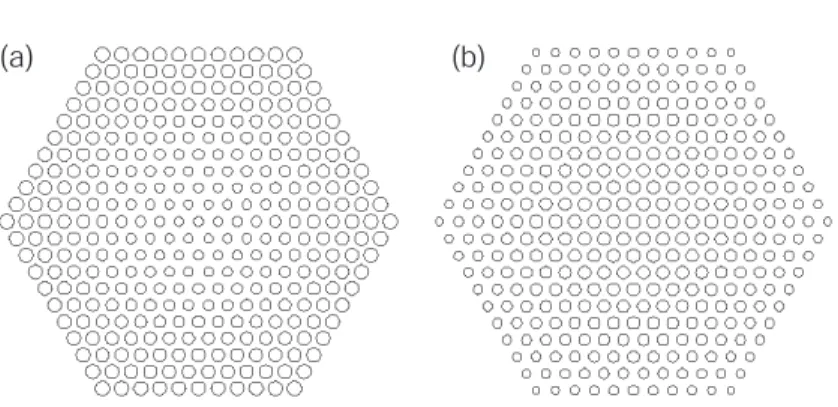
This was done both by changing the grating constant in some region of the waveguide [28] and by moving the position of a small number of holes within the structure [30]. For example, additional constraints on the mode volume and the robustness of the cavity geometry to imperfections could be added to such an analysis. The lattice specification may be dictated by the desire to create modes a.
Introduction
High Q photonic crystal microcavities in InAsP/InGaAsP multi-quantum wells in InAsP/InGaAsP multi-quantum well membranes. For the square lattice cavities studied in Chapter 2, one such mode is a donor-type mode (named A2 because of its symmetry) centered in the dielectric between two rows of air holes (point e in Fig. 3.1 ). Further improvements in both in-plane and vertical loss are achieved by classifying the mesh as shown in fig.
![Figure 3.1: (a) Graded square lat- lat-tice cavity designed in ref. [21];](https://thumb-ap.123doks.com/thumbv2/123dok/10413467.0/150.918.108.497.100.423/figure-graded-square-lat-lat-tice-cavity-designed.webp)
Fabrication of PC cavities in InP-based multi-quantum-well mem- branesbranes
- Mask creation
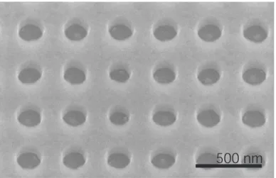
The requirements for the process were that the etched sidewalls were as smooth and vertical in slope as possible. To maintain the integrity of the ICP/RIE chamber, O2 plasma purges were periodically run between etchings. A scanning electron microscope (SEM) image of the etched SiO2 mask layer is shown in fig.
Photoluminescence measurements
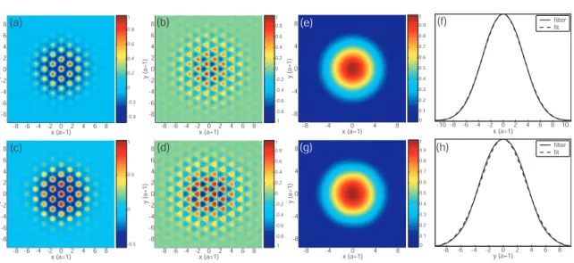
The generated Gaussian fits to the envelope of the cavity mode electric field energy density are shown for comparison (note that the effective mode volume is calculated from the peak electric field energy density). Lx and Ly correspond to the physical size of the PC in the ˆx and ˆy directions, respectively. 3.9(a) we show measurements of the emitted laser power as a function of the position of the pump beam (assuming this is the center of the beam) relative to the center of the cavity (uncertainty in the pump position is ~0.25 µm ).
Summary
The measurements indicate that the mode is highly localized at the center of the cavity, consistent with simulations. More importantly, the measurements we performed on these devices give us an indication of the limitations of these spectrometer-based studies using cavities fabricated in an active material. Most importantly, developing a technique to efficiently get light in and out of PC microcavities would make these devices much more functional and integrateable into more advanced experiments or systems.
Optical-Fiber-Based Measurement of an Ultrasmall Volume, High-Q Silicon
Introduction
In Section 4.8, I briefly review some of the work that I was not the principal investigator for but that I had the opportunity to be a part of and that is directly related to the work described in this and subsequent chapters. The first topic [57] describes the work of my colleague Paul Barclay in coupling light into our PC microcavities through the use of a PC intermediate waveguide matched to the phase of the fiber taper. The second topic I review is the work of Matt Borsell [64], who used fiber taper to investigate Si microdisk cavities.
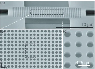
Fabrication
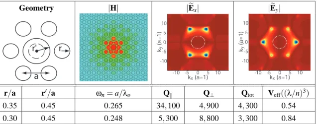
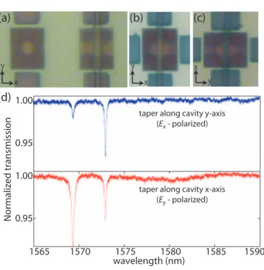
Undercut PC microcavities are fabricated in a linear array that is isolated from the rest of the chip by a few microns. The devices in (a) have the extra material removed along the ˆy axis of the cavity to allow alignment of the taper of the optical fibers along this axis. The combination of changing a and ¯r/a allows us to easily tune the cavity resonances through the range of the scanning tunable laser (λ=1565–1625 nm) that we use in our measurements.
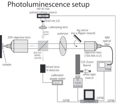
Measurement setup
The laser and photodetector output are connected to a computer via GPIB interfaces so that the wavelength-dependent transmission of the cone can be recorded. In addition, the motorized stages on which the taper and PC chip are mounted are also GPIB controlled, so that the taper transmission spectrum can be monitored as a function of the position of the taper relative to the cavity. When the taper is aligned laterally across the central region of the cavity and positioned vertically within the near field of the cavity (typically <1 µm), the cavity becomes.
Measurement results
- Polarization
- High-Q measurements
- Spatial localization measurements
When the cone is laterally aligned with the center of the cavity and vertically approaches it, we observe cavity resonances. The measured normalized cone transmission depth (black dots) is plotted as a function of cone displacement along (a) the ˆx axis and (b) the ˆy axis of the cavity. Plot of the normalized full width at half maximum (FWHM/(λ0/n)) of the dominant component of the conical electric field at the center of the PC plate, as a function of the normalized cone plate gap (Δz/λ0 ) and the cone diameter ( d/(λ0/n)).
Applications to quantum optics
Using measured Q and estimated Veff for the A02 mode studied here, the corresponding parameters for a commonly used Cesium (Cs) atomic transition (λ0=852 nm, γ⊥/2π=2.6 MHz) [9] and formulas (see appendix H). More detailed calculations using the optical bistability equation of state and the quantum master equation have been performed [62] and confirm that it should be possible to detect strongly coupled single atoms in this system. Furthermore, calculations of the coupling and decoupling parameters for an InAs semiconductor quantum dot [127] show that the actual PC microcavity would also be capable of achieving strong coupling in such a solid-state system.
Fabrication-tolerant high-Q cavities
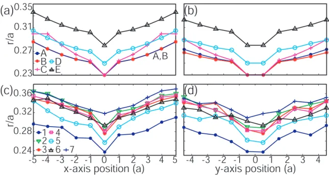
Here I focus purely on the response of the Q to variations in the size of the holes in the PC lattice. This customization was achieved in Chapter 2 by a degree in the hole radius moving outward from the center of the cavity. The transmission curves are normalized with respect to the transmission in the absence of the PC cavity.
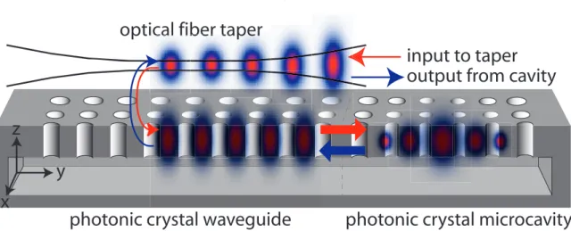
Fiber tapers as an optical probe for photonic crystal microcavities
In particular, the critical alignment step required in this work is to make sure that the taper is not slanted with respect to the surface of the chip, to ensure that coupling occurs only between the taper and the cavity, and not a foreign part of the slide. . Furthermore, the simplicity of the measurement technique is another attractive feature; a single fiber taper serves as both the excitation and collection probe, and the taper is physically robust enough (will not break) that no active servo control of the taper position is required to prevent it from touching the sample surface (in in contrast to the more delicate probes used in NSOM techniques [132]). Due to the low-loss nature of the optical fiber taper (insertion losses are frequently as low as 10%), however, this is still a significant amount of coupling in the cavity, and from the measurement point of view, coupling levels of a few percent are easy sufficient to distinguish cavity resonances in the taper's transmission, and to then investigate the Q and Veff of the cavity.
Efficient optical fiber coupling to photonic crystal microcavities and microdisksand microdisks
- PC microcavities
- Microdisk cavities
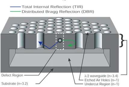
One solution is to integrate the cavity with an on-chip photonic crystal waveguide (PCWG), and then use various endfire-based approaches to couple in and out of the PCWG. Thus, light propagates through the PCWG, and when it reaches the termination of the PC cavity, some of the light that resonates with the cavity mode tunnels into it (the amount of tunneling can be adjusted by adjusting the PCWG-PC cavity junction ). ). This is a result of the large refractive index contrast between the Si layer (n∼3.4) and the surrounding air (n=1).
Fiber-Coupled Microdisk Cavities with Embedded Quantum Dots
The second part of this thesis studies the properties of AlGaAs microdisk cavities containing an integrated layer of self-assembled InAs quantum dots. For cavity QED experiments, the key findings from these chapters are that the demonstrated microdisc cavities have the necessary combination of Q and Veff for strong coupling to a single QD, and the fiber coupling technique provides an important tool that may enable future generations of experiments.
Optical Loss and Lasing Characteristics of AlGaAs Microdisk Cavities with
Embedded Quantum Dots
- Introduction
- Overview of microdisk cavity modes
- Analytic approximation
- Finite-element method simulations
- Standing wave whispering gallery modes
- Fabrication
- Cavity Q measurements in the 1400 nm band
The third equation is used to solve for the radial dependence of the cavity mode. It is assumed that the solutions of equation (5.10) with δε=0 (ie, the modes of the perturbed structure) are written as If we rewrite the coupled mode equations in terms of standing wave mode amplitudes, we arrive at:.