14 (a) Measured electrical and (b) thermal resistance of contact silver nanowires with Dh of 92 nm before and after welding. The L/L0 of the point contact and the single silver nanowire are also shown for comparison.
Phonon Transport in Individual Nanostructures
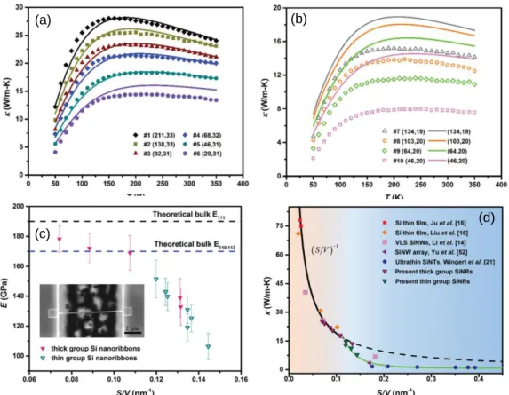
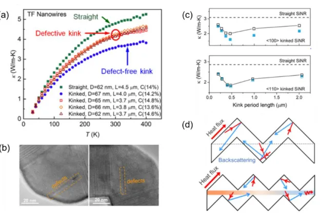
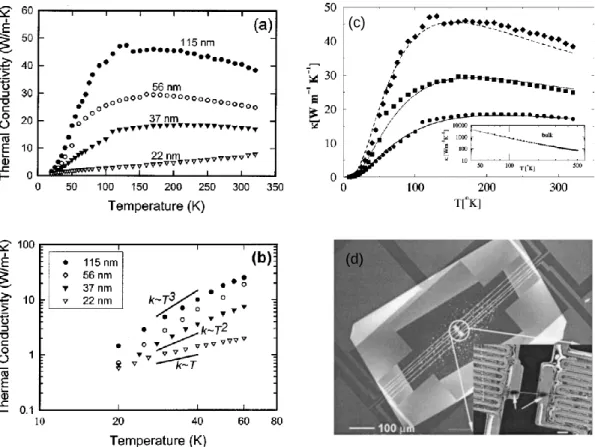
As shown in Figure 1.4(a), silicon nanomesh films fabricated by electron beam lithography possess a low thermal conductivity of ~2 W/m-K, which is two times lower than that of an array of silicon nanowires with ratios relatively larger S/V. (Yu et al. 2010). 7 (a) Thermal conductivity of boron carbide nanowires that are straight, defect-free bends, and defect bends, respectively (Zhang et al. 2017).
Contact Resistance between Individual Nanostructures
However, some studies show that the temperature dependence of the electrical resistance of semiconducting SWCNT-enriched and metal-SWCNT-enriched films follows FIT model (Blackburn et al. 2008). Previous studies have measured thermal resistance of metal interfaces (Gundrum et al. 2005; Wilson and Cahill 2012).
Summary
The results in Figure 3.14 show that the electrical and thermal resistance of the contact sample is greatly reduced after welding. The electrical resistance of the point contact between the two tubes was calculated using Eq.
Experimental Setup and Device Fabrication
Measurement Device
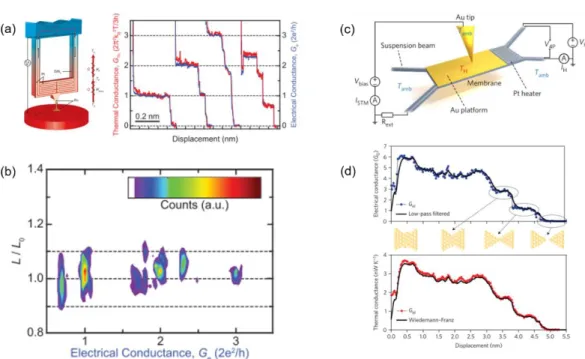
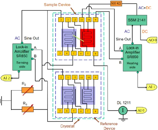
Each PRT is connected to four 400 µm × 500 µm Pt bonding pads on the substrate through the 1.5 µm wide Pt leads on the corresponding long SiNx beams. The electrodes on the microdevice can enable simultaneous four-point electrical resistance measurement and Seebeck coefficient measurements.
Device Fabrication
Wet etching of the exposed silicon substrate with TMAH to suspend the SiNx membranes and beams.
Sample Preparation
Pt/C deposits are used to increase the thermal and electrical contact between the nanowire and the electrodes. As shown in Figure 2.5, alcohol can diffuse at the interface between the nanowire and the membrane. A small amount of alcohol is dropped onto the membrane and diffuses to the interface between the nanowire and the membrane.
Measurement Setup
𝑄2 = 𝐺𝑏Δ𝑇𝑠 = 𝐺𝑠(𝑇ℎ− 𝑇𝑠), (2.1) where Δ𝑇𝑠 = 𝑇𝑠− 𝑇0 is the temperature rise of the sensing membrane and Gs is the thermal conductivity of the sample. The temperature rise of the sensor membrane is obtained from the output voltage of the Wheatstone bridge circuit. Unlike Rh, which is measured directly using the four-point method, the electrical resistance on the sensing side includes the resistance of the sensing PRT (Rc) and the resistance of two Pt leads (2RL).
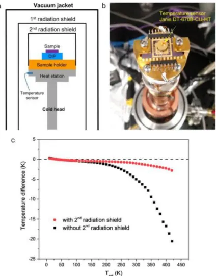
Effects of Radiation Shields
To check the effectiveness of the additional shield, a calibrated silicon diode sensor (Janis DT-670B-CU-HT with accuracy 0.1 K) is mounted on the DIP to measure the local temperature of the DIP with and without the second radiation shield , as shown in Figure 2.10(b). Then, the thermal measurement on the same silicon nanostrip with and without the second radiation shield was performed to examine the effect of the second radiation shield on the thermal conductivity. Without the second radiation shield, the measured electrical resistance of the heating PRT at 420 K is 4.2% lower than that measured with the internal radiation shield.
Background Thermal Conductance
- Effects of Background Thermal Conductance
- Rejection Mode
- Three-Membrane Device
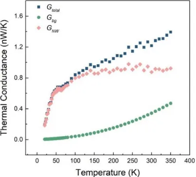
However, with increasing temperature, the background thermal conductivity increases rapidly following the T4 law and at 350 K the background thermal conductivity (~470 pW/k) is almost half of the sample thermal conductivity (~920 pW/K). We fit the measured thermal conductivity of a blank device with the fourth-order polynomial temperature function and consider it as the background thermal conductivity for that set of devices with the same gap distance. As shown in Figure 2.14, during measurement, the sensing and reference membranes receive the same radiant heat from the heating membrane; with the Wheatstone bridge connected to the sensor and reference sides, the background thermal conductivity can be effectively canceled.
Summary
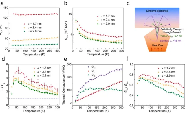
The ratio of the thermal contact resistance to the intrinsic thermal resistance of the nanowire (Ri = Ls/A) is proportional to (Dh)1/2/Ls, which is lower for smaller wires. When lattice thermal conductivity is neglected in the 84 nm nanowire, the Lorenz number of the nanowire, 𝐿𝑛𝑤 ∝𝑙𝑡ℎ,𝑛𝑤. As a comparison, we also plotted the total electrical resistance of the contact CNTs in Figure 4.3(b).
Electrical and Thermal Transport through Silvers Nanowires and Their Contacts
Sample Preparation and Characterization
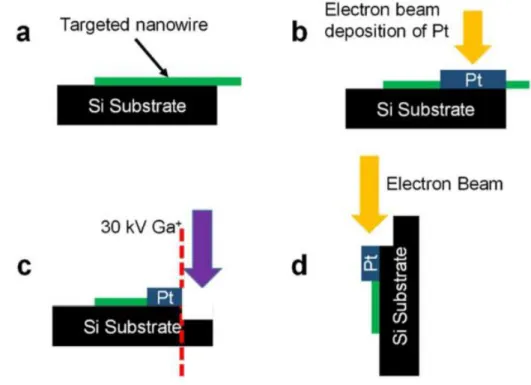
A focused ion beam (FIB) was used to etch a portion of the nanowire and expose a cross-section of the sample. The cross-section on the right corresponds to the pattern shown on the left. The cross-sectional cutting method is also used to examine the contact configuration between two silver nanowires.
Wire-Membrane Contact Effect
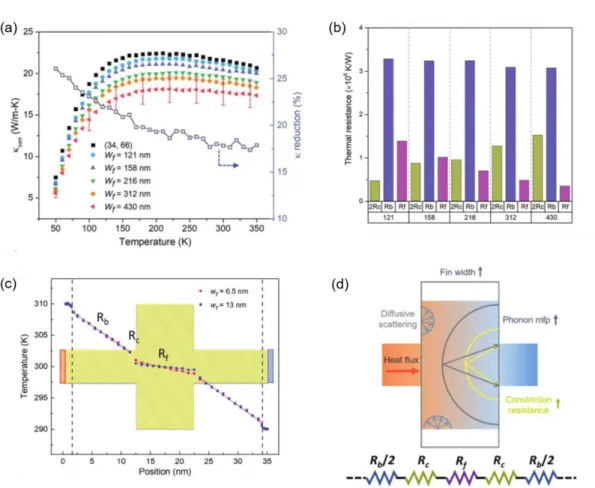
As shown in Figure 3.4(d), EBID can significantly reduce the contact thermal resistance between the nanowire and the suspended membranes; however, the thermal conductivity still increases slightly (< 10%) after the second round of EBID, indicating that the contact thermal resistance does not drop to a negligible level. Based on a fin model (Bifano et al. 2012), the thermal contact resistance (RCTR) with each membrane can be expressed as. The fact that the second round of EBID does not change the thermal resistance of the contact suggests that the RCTR is independent of the contact length.
Bending Effect
Therefore, it is reasonable to assume that with EBID the effects of thermal contact resistance become trivial for silver nanowires with Dh < 90 nm and Ls > 40 µm. A silver nanowire with a diameter of 65 nm (a) without and (b) with an artificial buckling defect between the two suspended membranes. c, d) Measured thermal and electrical conduction resistance before and after the kink is introduced.
Temperature Dependence of Transport Properties
Another factor that may contribute to the lower thermal conductivity in the literature is the wire diameter rating. The temperature dependence of the electrical resistance of the same wire is shown in figure 3.7(b). However, as the temperature decreases, the Lorenz number of the nanowire deviates from the main value with higher values for the nanowire.
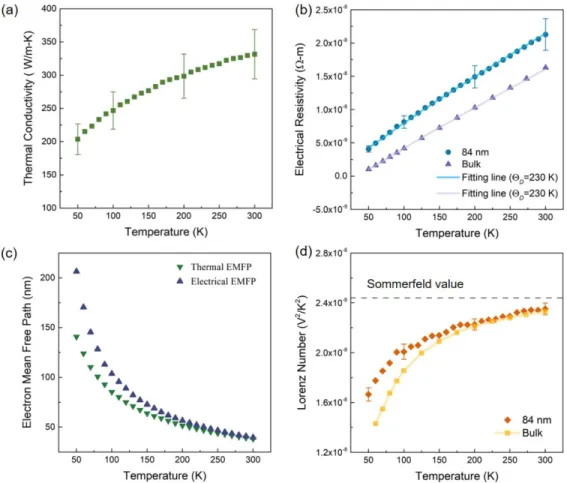
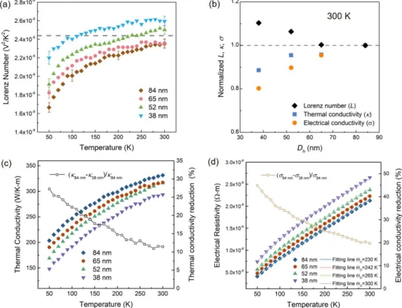
Size Dependence of Transport Properties
By subtracting the lattice thermal conductivity from the total thermal conductivity, the Lorenz number due solely to electron transport (Le) can be derived as 𝜅𝑒/𝜎𝑇. The overall effect is significantly improved lattice thermal conductivity, making an effective Lorenz number higher than the Sommerfeld value for small silver nanowires. In fact, if we take the room temperature Lorenz number due solely to electron transport as the Sommerfeld value, the lattice thermal conductivity for the 38 nm wire can be derived as 17.5 W/m-K, over three times the bulk value of 4.6 W/m-K .
Transport at the Contact between Two Individual Silver Nanowires
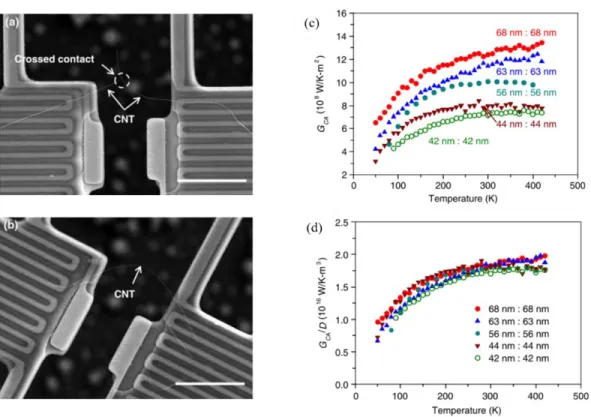
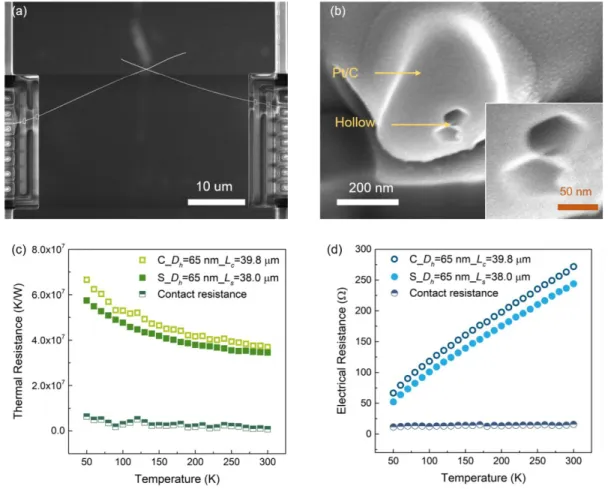
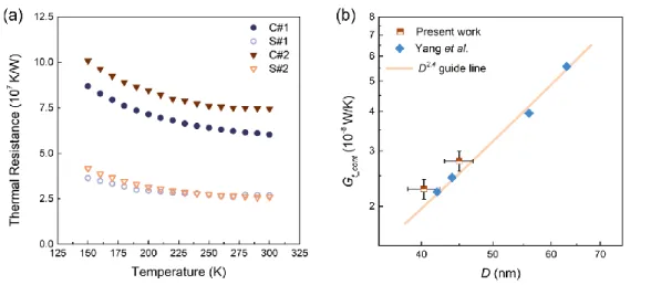
The contact resistance, RC, can be derived from RC = Rt,contact ˗ Rs/Ls×Lc, where Rt,contact. The contact electrical and thermal resistances are also shown in Fig. 3.12(c) and (d), which are approximately one-tenth of the measured total resistance of the individual and contact samples. For example, at 300 K compared to a contact thermal resistance of ~1.8 × 10⁷ K/W between two 63 nm diameter MWCNTs as reported by Yang et al.
Effective Lorenz Number of the Point Contact between Silver Nanowires
Therefore, instead of deriving L/L0 for the spot contact, we calculated L/L0 for the contact sample before and after welding. As shown in Figure 3.15(d), before welding, L/L0 of the contact sample shows a temperature dependence similar to that of the point contact, but with lower values. After welding, the L/L0 of the contact sample almost overlaps with that of the single silver nanowire, indicating that compared to the nanowire segments, the electrical and thermal resistance of the point contact are marginal.
Summary
Pressure Dependence of Resistivity of Single-Walled Carbon Nanotube Ropes." Physical Review B - Condensed Matter and Materials Physics. Mechanism of Reduced Thermal Conductivity of Si-type Herringbone Phononic Crystal Nanostructures." Journal of Electronic Materials. Measurement of the internal thermal conductivity of a multiwalled carbon nanotube and the thermal resistance of its contact with the substrate. Small.
Thermoelectric Properties of Individual Contacts between Multiwall Carbon Nanotubes
Sample Preparation
The thermal measurement was performed following the well-established approach in a high-vacuum cryostat system (<10-6 mbar) using a microdevice with prepatterned platinum electrodes and resistance heaters/thermometers (Yang, Tao, et al. 2019; Zhang et al. 2017; Zheng et al. al. 2013). The platinum electrodes on the side of the membranes make it possible to perform four-point electrical measurement and Seebeck coefficient measurement. A very long multiwall CNT was cut into three segments, two of which were used to form the contact sample and the third part as the corresponding single CNT segment.
Thermal and Electrical Transport Properties of the Point Contact
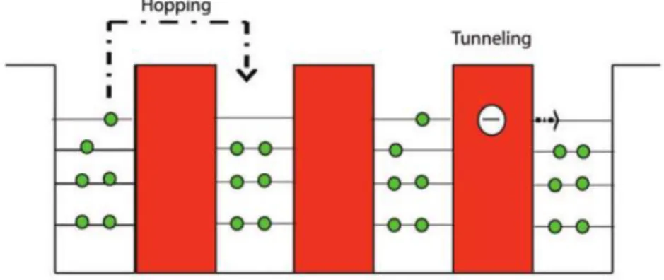
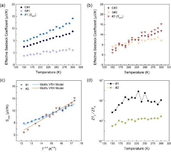
It should be noted that the electrical resistance of the point contact occupies ~35% and ~60% of the total resistance of samples C#1 and C#2, respectively. a) Measured electrical resistance of the contact and individual CNTs. In the VRH model, the parameter T0 can be extracted from a linear fit for the contact electrical resistance and the expression for T0 can be written as The dimensionality of the hopping can be determined by the hopping distance and c-axis size of the contacting CNTs; since the hopping distance is smaller than the c-axis size of the contacting CNTs, the hopping electron transport is 3D (Yosida 1999).
Thermoelectric Properties of the Point Contact
With the measured thermal resistance, electrical resistance and Seebeck coefficient, the thermoelectric efficiency was estimated by the dimensionless ZT. Although the thermal and electrical conductivity can be largely reduced by the tube contact, the ZT of the C#1 sample is improved by almost two orders. However, due to the similar Seebeck coefficient of the single CNT and the point contact for the C#2 sample, the ZT enhancement is only about twice as large.
Summary
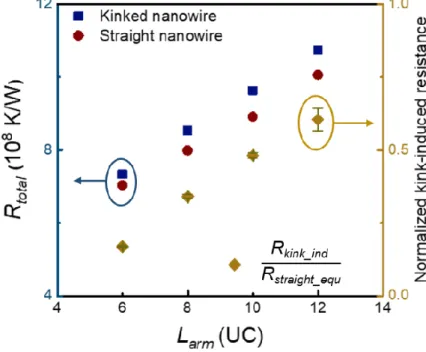
𝑅𝑠𝑡𝑟𝑎𝑖𝑔ℎ𝑡_𝑞𝑢 = 𝑅𝑡𝑜𝑡𝑎𝑙_𝑠𝑡𝑟𝑎𝑖𝑔ℎ𝑡× 𝐿𝑘𝑖 𝑛𝑘⁄𝐿𝑡𝑜𝑡𝑎𝑙, (5.3) where Rtotal_kinked and Rtotal_straight are the total thermal resistance of bent and straight nanowires. The arm length dependence of the kink-induced resistance, Rkink_ind, is also related to phonon scattering in the kink. Modeling the Elastic Properties of Crystalline Silicon Using Lattice Dynamics.” Journal of Physics D: Applied Physics.
Kink Effect on Thermal Transport in Silicon Nanowires
Non-Equilibrium Molecular Dynamics Simulation Method
𝑇 2⁄ and 𝑇0− ∆𝑇 2⁄ respectively, where 𝑇0 is the equilibrium temperature of 300 K and ∆𝑇 is the temperature difference of 60 K between the two reservoirs. The linear adjustment slope of heat transfer as a function of time is the average heat transfer rate, qave. The phonon DOS is calculated from the Fourier transform of the velocity autocorrelation function as (Sokhan, Nicholson and Quirke 2000).
Simulation Model of Straight and Kinked Silicon Nanowires
During the simulation, after the steady state is reached, the heat added to the hot reservoir, QH, and that subtracted from the cold reservoir, QC, are collected every 10 ps. The amount of heat transferred from the hot reservoir to the cold reservoir is calculated by averaging the absolute value of QH and QC. With the velocity of three different directions obtained from the simulation, the phonon DOS can be extracted for longitudinal and transverse modes, respectively.
Thermal Transport in Straight and Kinked Silicon Nanowires
The temperature profile of the straight nanowire is linear along the entire length of the wire, which is consistent with our expectations. On the other hand, the temperature gradient in the two arm regions of the bent nanowire is larger than that in the corresponding straight nanowire. Proving the smaller temperature drop, the thermal resistance of the bending segment in bent wires is less than that of a 4 UC segment in straight wires; however, armature resistance is greater than that in straight wires.
Theoretical Analysis on Thermal Transport in Kinked Silicon Nanowires
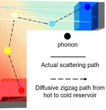
Only when phonons are scattered in the kink and deflected in the opposite arm can they carry energy to the opposite thermal reservoir. For shorter arm length cases, the chance of phonons moving into the kink region is greater than that for larger arm length cases. Thus, as the arm length extends, the kink-induced resistance escalates, as shown in Figure 5.2.
Defect Effect on Phonon Transport in Kinked Silicon Nanowires
- Simulation Model of Straight and Kinked Silicon Nanowires with Defects
- Effect of Elastic Anisotropy on Phonon Transport in Kinked Nanowires
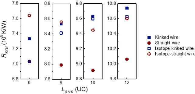
This result is consistent with the experimental observation from the boron carbide nanowires (Zhang et al. 2017), again suggesting that phonon scattering in the kink helps phonons make the turn and facilitates thermal transport through the kink. The results indicate that the phonon DOS of the 42Si and 28Si atoms has only a marginal difference in the straight and broken nanowires. The slightly smaller NEMD value could be attributed to the smaller system size in the simulation, as the kink-induced resistance increases with arm length in our MD results.
Summary
Thermal Conductivity of Germanium Crystals of Different Isotopic Compositions." Physical Review B - Condensed Matter and Physics of Materials. Effects of Heat Treatment and Contact Resistance on the Thermal Conductivity of Individual Multiwalled Carbon Nanotubes Using a Wollaston Wire Thermal Probe." Journal of Applied Physics. Kink as a New Degree of Freedom for Tuning the Thermal Conductivity of Si Nanoribbons.” Journal of Applied Physics.
Summary
SEM micrograph of the suspended microdevice with electrodes and integrated
Schematic diagram of the fabrication process. (a) Bare silicon wafer. (b) LPCVD deposition
A photograph of an in-house assembled micromanipulator mounted with a sharp tungsten
SEM micrograph of an individual silver nanowire bridging two suspended membranes with a
Wetting process. A small amount of alcohol is dropped onto the membrane and spreads to the
Schematic diagram of the measurement setup
Thermal circuit of the measurement scheme
Simplified electrical measurement circuit for both the heating and sensing sides
Schematic diagram of Seebeck coefficient and four-point electrical resistance measurement
Effects of the inner radiation shield (Yang 2019). (a) Schematic drawing showing the inside
Comparison of measured quantities using single and dual radiation shield set-ups (Yang et al
Measured total thermal conductance (G total ), background thermal conductance (G bg ), and