Finally, I would like to thank Jesus Christ, who taught me to be a moral person, and God, who gave me life. My contribution was to help fabricate these thermoelectric devices, and this is the focus of this part of the thesis. The second part and primary focus of this thesis is the analysis of thin films using scanning probe techniques.
Nanostructured Silicon Thermoelectrics
Introduction
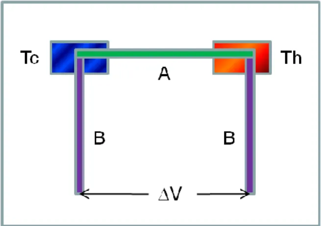
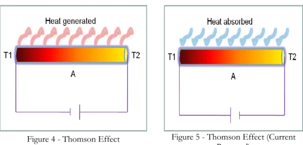
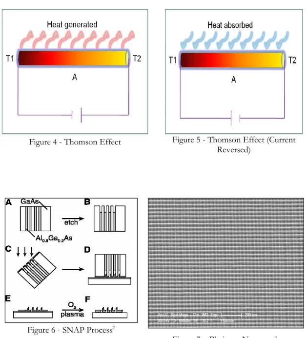
The ratio between the voltage potential and the temperature difference is called the thermopower, or S.1 The Seebeck effect can also be observed in semiconductors. It is therefore commonly called “the opposite of the Seebeck effect” and is shown in Figure 2. Both the pitch and diameter of the wires can be changed by using a different SNAP master.
Experimental Methods
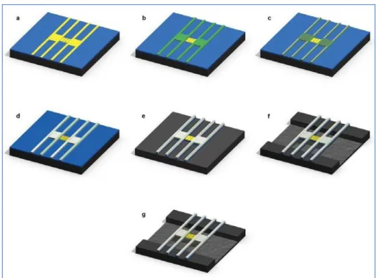
An Al etch mask is placed on top of the device to protect it further. Another Al etch mask is then placed over the silicon nitride layer and patterned to match the device platform. Similarly, another metal mask, Al or NiCr, is placed on top of the parylene layer and on the device platform.
Phononic Model
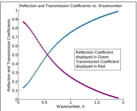
When this happens, phonons propagating through the structure will have to "bend" around a corner in order to reach the other end of the nanostructure. A significant fraction of phonons is expected to be reflected when this occurs. For large values of the wave number, the reflection coefficient is large, while the transmission coefficient is low.
Figures
The scale of the device is exaggerated from reality for better visualization. a) Silicon nanomesh with monolithically defined silicon device platform.
Atomic force microscopy characterization of layers of small organic molecules at room temperature through graphene template.
Introduction
We use graphene sheets as an ultrathin coating/template for the atomic force microscopy (AFM) characterization of the room-temperature structures of the adlayers at the interfaces between mica surfaces and small organic molecule vapors. In the current work, we show that graphene, even though it is only one atom thick, can prevent the evaporation of molecularly thin layers of volatile small organic molecules and slow down the movements of the molecules on the solid surface, allowing AFM observation of both becomes possible. the structure and dynamics of the adlayers at room temperature. Two common small organic molecules, tetrahydrofuran (THF) and cyclohexane, each representing one of two classes of polar and nonpolar organic solvents, were examined and compared with water.
Experimental Methods
A confocal optical microscope with a 100x objective lens was used to record spectra with a spatial resolution of 2 μm. Due to the super-flatness of the samples, sometimes the laser interference pattern along the axis of the slow scan was difficult to avoid, which is more obvious in the large-area scan and has a period of twice the wavelength of the laser. This is caused by the constructive interference of the laser reflected from the surface of the sample with that reflected from the cantilever.
Results and Discussion
The boundaries of the islands formed by the first THF adlayers often appear rounded (Fig. 1b–d). As with THF, the height of the first adlayer of cyclohexane is statistically thinner than the second adlayer: the uncertainty in height is ignored. For example, the height of the first layer may be slightly smaller than the layer thickness in the plastic crystal structure.
Conclusions
One possible explanation of our result is that the THF adlayers are in a "hexatic" phase that is between the solid and liquid phase; while in three.
Figures
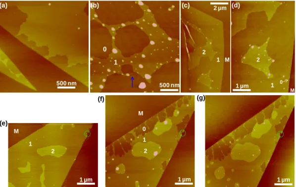
M labels the mica surface, and 0, 1, and 2 label areas where monolayer graphene sits on top of 0, 1, and 2 adlayers of cyclohexane, respectively. The green circle marks a defect on the graphene edge, which served as a reference point when aligning the images. Similar Raman spectra were also observed for monolayer graphene sheets deposited on mica surfaces in equilibrium with cyclohexane vapors.

Scanning tunneling and atomic force microscopy probes of self-assembled, physisorbed monolayers: Looking at the tips. Low-energy electron diffraction study of the surface of thin crystals and monolayers of normal paraffins and cyclohexane on the Ag(111) crystal surface. Coexistence of liquid and solid phases of Bmim-PF6 ionic liquid on mica surfaces at room temperature.
The Microscopic Structure of Adsorbed Water on Hydrophobic Surfaces
- Introduction
- Experimental Methods
- Results and discussion
- Conclusions
- Figures
For Si(111) surfaces with H terminology, we found that the contrast of graphene sheets can be improved by proper filtering of the micrographs obtained with a CMOS camera. For Si(111) surfaces with H terminology, we found that the contrast of graphene sheets can be improved by proper filtering of the micrographs obtained with a CMOS camera. The identification of deposited graphene on all three substrates enabled the extension of the graphene templating technique to hydrophobic surfaces.
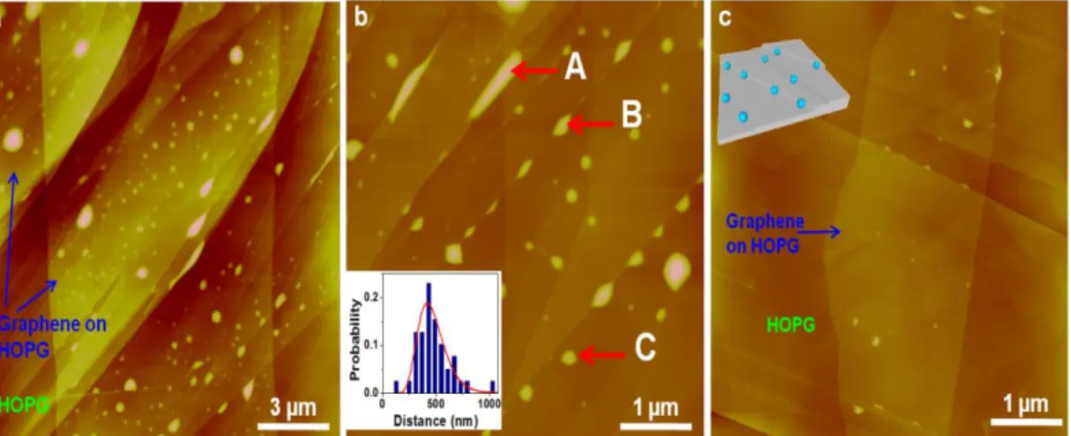
These results show that the graphene templating method can trap highly diffusible water molecules, thus allowing a map of adsorbed water on the HOPG surface. The exact height varies and is not a multiple of the bilayer height in ice crystals (0.37 nm)15, implying that the adsorbed water nanodroplets are liquid. A close inspection of the TMCS-functionalized mica surface itself (Fig. 3c) shows that the surface is characterized by randomly distributed atomic-scale inhomogeneities that are not present on the as-cleaved (non-functionalized) surface (Fig. 3d).
Fourier transform images (insets in Fig. 3bc) further show that the distribution of water nanodroplets (as visualized by graphene templating) and the distribution of domain-like structures on the TMCS-functionalized mica surface correspond to a characteristic length of ~75 nm in lateral dimensions (Fig. 3f). The volume integration of the nanodroplets gives about 40% monolayer coverage for adsorbed water on the TMCS-mica surface. This % coverage is comparable to that on hydrophilic mica surfaces, although the surface structure of water is very different.
The reduced θ is often attributed to the effects of the contact line tension (), which is one-dimensional.
Raman shift (cm-1)
- References
- Introduction
- Experimental Methods
- Results and Discussion
- Conclusions
- Figures
- References
The nature of water on surfaces of laboratory systems and implications for heterogeneous chemistry in the troposphere. Evaluation of the wettability of metal surfaces by micropure water by means of atomic force microscopy. The meaning and magnitude of the line voltage in three-phase (solid-liquid-liquid) systems.
In the previous two chapters, the graphene templating technique has been shown to be applicable to the templating of different substances as well as different substrates. These include pH, temperature, concentrations of salts in carrier solvents, and others.4,5 Techniques such as x-ray crystallography can provide a lot of information about these molecules, but can be quite difficult to perform. A piece of graphene-covered adhesive tape was first prepared using Kish graphite flakes, and set aside for subsequent exfoliation on mica substrates.
The previously prepared graphene-covered tape was then used to exfoliate graphene on the mica disks, and an optical microscope was used to find suitable single-layer graphene samples. The structures are clearly resolved in both graphene-covered and non-graphene-covered regions of the sample. STM, which can deliver Angstrom resolution in all spatial dimensions, could potentially provide some of the most detailed images of biomolecules ever created.
An exciting prospect is the use of STM to image the graphene-coated biomolecules and perhaps even investigate their perturbing effects on the electronic structure of graphene.

Scanning-Tunneling Studies of Graphene-templated Water
- Introduction
- Experimental Methods
- Results and Discussion
- Conclusions
- Figures
- References
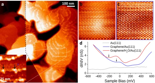
At the opposite end of the spectrum, a uniform local doping level with no spatial features has been observed for graphene deposited on atomically flat boron nitride. The water clusters were likely initially adsorbed on the ladder edges of the gold islands under ambient conditions,19 while the application of graphene trapped and fixed the clusters. We interrogated the influence of trapped water clusters on the local electronic structure of graphene using STS at ~77 K to measure the differential local tunneling conductance, dI / dV.
Variations in the position of the depression feature thus reflect changes in local doping levels. To determine the local doping level, we investigated the local energy positions of the Dirac point (ED = eVD) by examining the positions of depression features (VD) in the dI/dV curves obtained at each site. This displacement increases sharply at the edge of the cluster and flattens out at the top of the cluster.
These results indicate that the shift in the Dirac point is induced by the trapped water clusters and that this shift is dependent on the size of the water cluster. Black arrows point to the positions of depression features (VD) corresponding to the Dirac point. Bottom panel: the local energy position of the Dirac point, ED = eVD, along the three arrows in (a).
The size of the trapped water clusters is shown by the number of red disks.
Scanning Probe and Photoluminescence Studies of Single-layer Molybdenum Disulfide*
- Introduction
- Results and Discussion
- Experimental Methods Identification of few layer MoS 2 Identification of few layer MoS2
- Figures
- scale: A) 4 nm, B) 3 nm C) 3°, D) 0.15 V, E)
- References
We find that water plays a significant role in changing the structure of the thin films, the local electric field gradient and. The height of the ad layers on the mica surface was approx. 1 nm - the height of a few layers of water. Investigating the electronic properties of the MoS2-water-mica system is very interesting and much.
Any measured shifts in the electronic spectra must therefore reflect the influence of the underlying water. Since the same material – single layer MoS2 – is being investigated, the potential difference is an indication of the change in the Fermi level of the sample. The presence of water raises the Fermi level of MoS2 relative to the Fermi level of the material when no water is present.
The vertical to horizontal aspect ratio (height to diameter) of the droplets ranges from approximately 0.05 - 0.5. Small particles appear to be ubiquitous at the edges of the thicker multilayered MoS2. The importance of the substrate in determining the electronic properties of the material is clearly illustrated.
Topography can affect the electric field, as surface curvature is directly proportional to surface charge density.

Activation and Degradation of Akt in Live Cells*
- Introduction
- Results and Discussion
- Conclusions
- Figures
We also functionalized the capture agents with other moieties and analyzed their effects on cell biology. We have shown that we are able to induce the activation of the target protein pathway and the degradation of the Akt protein in vivo. The acidic peptide solution was neutralized using 2 equivalents of DIEA, followed by removal of the solvent by rotary evaporation.
The resin was treated with 2 equivalents of the alkyne in question, 1.5 equivalents of CuI (Sigma) and 2.5 equivalents of ascorbic acid (Sigma), in a solution of 20% piperidine in DMF. The structure of the TAT-bound N-terminal capture agent is shown in Figure 1, where the HIV TAT sequence of the capture agent is separated by two PEG spacers and a protected lysine residue that can be further functionalized as desired (addition of a dye) , etc.). To validate cellular uptake, we treated U87 cells with fluorescently labeled capture agent and acquired simultaneous fluorescence and transmission images.
Thus, the N-terminal capture agent is able to significantly activate the Akt protein even in the absence of cellular phosphorylation. Figures 6 and 7 show the structure of the N and C-terminal triligands with the VHL binding site from the hypoxia-inducible factor 1α protein. The N-terminal capture agent (blue) is separated from the TAT sequence (red) by two PEG spacers and a lysine residue that can be further functionalized.
The higher magnification makes it possible to see cellular features such as the nuclei of the cells.
Days
SKOV3
OVCAR3