Sandy Weireb and Professor Harry Atwater for their invaluable time in my thesis defense and constructive comments. Jie Yu and Ronald Hlavac of Conexant Systems for their help during all tape-outs.
High Frequency and Wideband
In the next decade, wireless communications promise to become the locomotive driving the electronics industry, just as personal computers and the Internet did in the 80s and 90s [1]. Therefore, an arguably more fundamental solution is to move to higher frequencies where more bandwidth is readily available.
High Frequency and High Speed
Technological progress is changing these assumptions and erasing the boundaries between these two areas. In this context, we want to address the challenges of silicon-based high-frequency/high-speed IC design to show that the same analog circuit techniques and methodologies can be successfully applied to both areas.
System-on-a-Chip
Each module can be individually designed and optimized for the target process technology to achieve the best performance. It is critical to study the design of high-frequency/high-speed communication circuits in the context of SoC.
High Power Efficiency
For example, in a system-on-board radio, extra buffers are added between the off-chip VCO and the on-chip mixer to compensate for parasitics and match the 50-ohm interface, even though both circuits may have high internal impedances. Second, there is no need to convert to 50-ohm RF subsystems, so lower signal power and fewer buffers are required.
Why Silicon?
Therefore, instead of simply optimizing conventional circuit topologies, new circuit techniques must be explored to achieve high energy efficiency.
Challenges
Therefore, it is necessary to develop new design methodologies that can take these limitations into account and achieve successful and robust designs despite the inaccuracies. Circuit prototypes were successfully implemented using CMOS and SiGe BiCMOS technologies and demonstrated new circuit techniques and design methodologies.
Organization
We have developed several new circuit techniques along with design methodologies, namely distributed voltage-controlled oscillators with current steering delay-balanced tuning (10 GHz and above), injection-locked frequency dividers with shunt peak amplification (19 GHz), self-dividing oscillators (21 GHz), and distributed transverse equalizer (10 Gbps). In this chapter we introduce two important circuit techniques, namely distributed circuit and injection closure, which form the two main themes in this work: the distributed circuit technique is applied in voltage-controlled oscillators (Chapter 3) and transverse rectifiers (Chapter 4); the injection locking technique is applied to frequency dividers and a new type of oscillators (Chapter 5).
Distributed Amplifiers
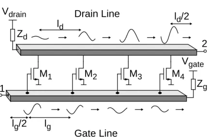
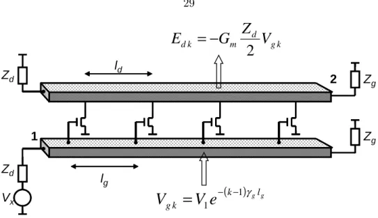
This maximum achievable gain-bandwidth product (Bode-Fano Limit [37]) is therefore mainly determined by the intrinsic parameters of the devices. Note that the voltage at the kth branch of the gate line (vgk) is related to the gate line segment length, lg, and the complex propagation constant of the charged gate line, γg, through [39].
Oscillators
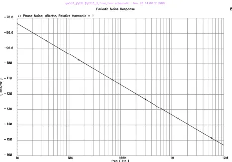
Phase noise is usually measured using the power spectral density (PSD) function of the output signal around the oscillation frequency. From (2.20), we can see that the phase fluctuation at low frequency ωm is up-converted to ω0±ωm, or equivalently, the oscillation signal is modulated by the phase fluctuation.

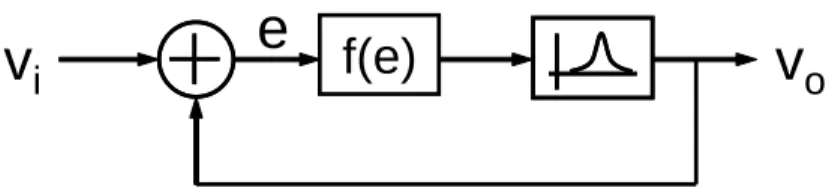
Injection Locking
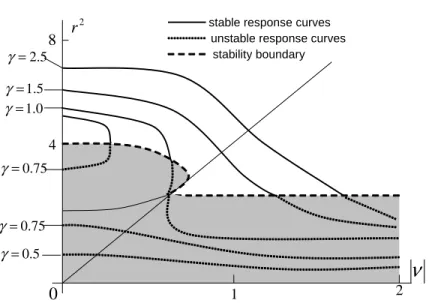
When γ >1.18, and ν small enough, the system has only one stable equilibrium point, and thus injection blocking can be established. The instantaneous frequency of the oscillator can be found from the phase-frequency relationship of the resonator.
Summary
The motivation behind distributed oscillators is introduced in Section 3.1, followed by the basic architecture and analysis in Section 3.2.3. Two new tuning techniques, namely inherent varactor tuning and current-controlled delay-balanced tuning, will be demonstrated in Section 3.3, which can realize distributed voltage-controlled oscillators (DVCOs).
Voltage-Controlled Oscillators
The design and layout issues of DVCOs will be discussed in Section 3.4, followed by experimental results from several prototypes, including a 10 GHz CMOS DVCO and a 12 GHz bipolar DVCO, in Section 3.5. On the contrary, resonator-based oscillators offer better phase noise performance for a given power dissipation.
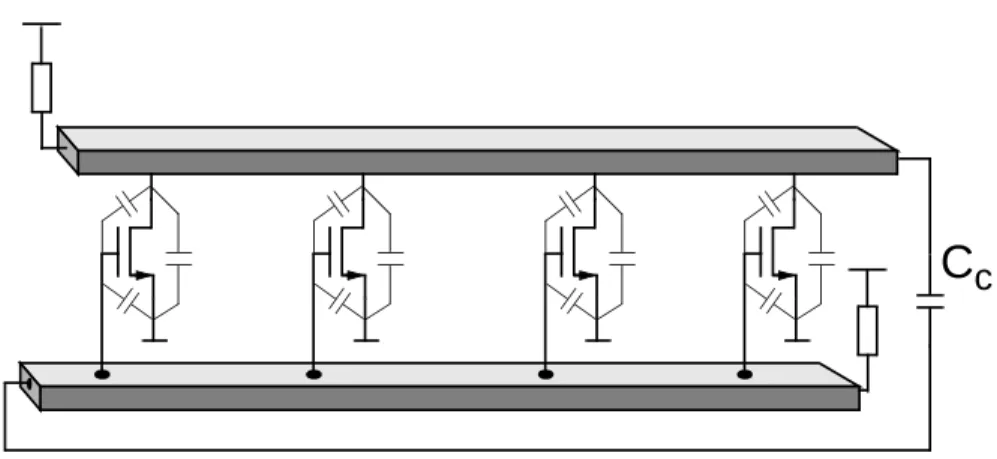
Distributed oscillators
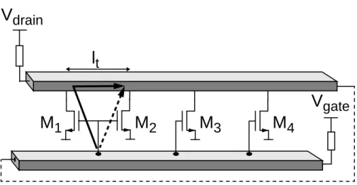
3.3, it is immediately clear that with a proper selection of the number of stages, a distributed oscillator can generate multiphase signals. Intuitively, the oscillation frequency is determined by the round-trip time delay, i.e. the time it takes for the wave to travel through the transmission lines and then be amplified by one of the transistors.
Tuning techniques
3.6, where the gates of M1 and M2 are connected to the same point on the gate line while separated on the drain line. Therefore, the traveling wave on the drain line will lag the gate wave in phase. In other words, it weakens the synchronization of the waves on the gate and drain lines.
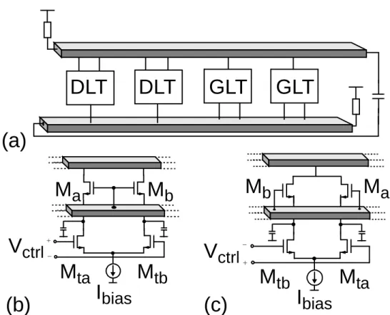
Design of DVCO’s
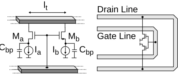
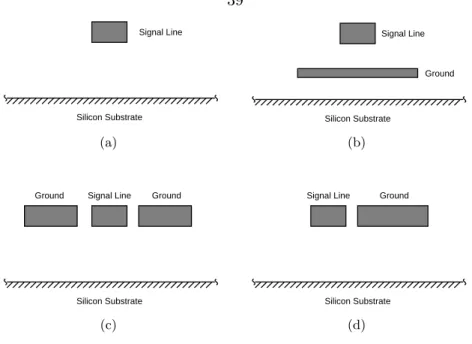
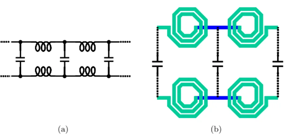
For DVCOs, it is desirable to find a special type of on-chip transmission lines that have low losses and high impedance5. Once the appropriate type of on-chip transmission lines is determined, the next important question is how to properly pattern them [68]. Asitic [72] is a special program to simulate on-chip inductors using Green's Functions and adapted for silicon substrate.
DLT DLT GLT GLT
GLTDLT
Measurement and Experimental Results
- CMOS DVCO
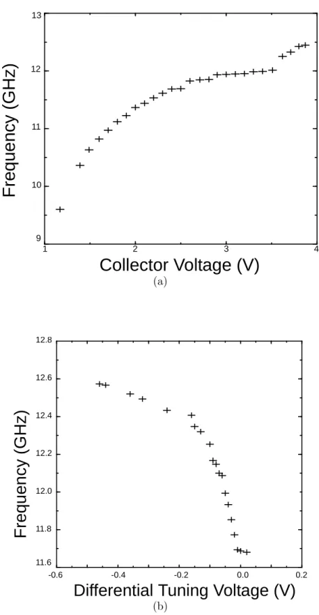
A tuning range of GHz) can be achieved using the inherent varactor tuning with a total drain current of 14 mA. The output power variation is 2.7 dB over this tuning range. The measured tuning range of the delay-balanced current control tuning technique is 2.5% around the center frequency set by the inherent varactor tuning, as shown in Figure. The delay-balanced current control tuning achieves a tuning range of 7.4% around the center frequency set by the inherent varactor tuning, as shown in Fig.

Alternative Architectures of Distributed Oscillators
This is a general problem in RF circuit design, but it is particularly difficult in the case of a distributed oscillator because of the relatively long distance between the ground nodes of the transistors. So there are no more distinct current lines as in the conventional distributed oscillator architecture. However, a TWA buffered distributed oscillator has multiple taps as interfaces between the distributed oscillator core and the buffered outputs.
Summary
Such an injection-locked distributed oscillator can be used for frequency synthesis, serving as both quadrature VCO and high-speed prescalar. Due to the wideband nature of distributed circuits, it is also possible to generate multiple frequencies that are harmonically related, i.e. the DVCO has multiple modes. Dispersion compensation techniques in optical and electrical domains are discussed in Section 4.2, and integrated transverse equalizers are presented as a promising solution to the challenges in high-speed equalization in Section 4.3.
Inter-symbol interference and dispersion
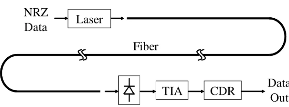
Instead, ISI becomes a bottleneck in long-haul high-speed fiber optic systems due to rapid advances in data rates and the widespread use of wavelength division multiplexing (WDM). However, it is obvious that the dispersion limit decreases with R2b from (4.3), which means that it shrinks to 1/16 for each generation of optical fiber systems whose bit rate increases by 4 times each generation. Since the introduction of erbium-doped fiber amplifiers, optical fiber systems have begun to transition to the 1.56 µm transmission window, in which erbium-doped amplifiers are more efficient than the 1.3 µm transmission window.
Dispersion Reduction
Polarization mode dispersion (PMD) [85][84] occurs due to the speed difference between the two polarization modes in single-mode fibers, which can be caused by fiber asymmetry, fiber bending, temperature variation, etc. PMD is proportional to the square of the bit rate and the square root of the distance, and is usually given in ps/√. However, due to the high installation costs, dispersion-shifted fibers make up only a small part of the global fiber optic networks.
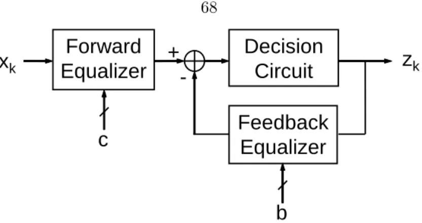
Distributed Transversal Equalizer
A decisional feedback equalizer [94][95] is a non-linear equalizer and usually consists of a forward equalizer and a feedback equalizer, which may be a cross equalizer (Figure 4.5). In fact, it can be considered as a traveling wave amplifier operating in feedback mode. Equalization coefficients can be realized by the gain from each stage, so it is inherently flexible.
Design
This makes it very difficult to maintain the same load on transmission lines from all levels at all times, ie. the transfer function itself tends to disturb the distributed characteristics of the circuit. The gain stage function in the transversal filter is the implementation of the equalization coefficient (weight). The weight sign is implemented using two differential pairs (Q3, Q4, Q5 and Q6) to route the differential current from Q1 and Q2 to the output transmission lines.
Measurement Results
This generated a signal with 5dB ISI at the input of the equalizer, while the equalized signal has a residual ISI of only 1.38dB. Also note that the equalization operation did not degrade the jitter performance – the deterministic jitter was actually reduced from 62ps to 38ps. Similar to the previous case at 10Gb/s, the signals are recorded at the input of the equalizer, the output of the equalizer with only one coefficient active and with two coefficients active to reduce the ISI penalty.
Future Improvements
Summary
After introducing the high-speed frequency divider design problem and different categories of frequency dividers in Section 5.1, ILFDs are presented as a promising solution, followed by the analysis in Section 5.1.3. Two prototypes of the ILFD division-by-2 with shunt-peak switching range extension are demonstrated in Section 5.2. Finally, a new type of low-noise quadrature oscillators, self-separating oscillators, will be presented in Section 5.4.
Challenges in High-Speed Frequency Dividers
Dynamic digital dividers can be implemented by removing the regenerative pair from the static dividers in Figure 5.3. For example, digital dividers in frequency synthesizers increase the noise floor and thus reduce phase noise at large offset. In addition, its noise level is also improved, as it is more energy efficient than digital dividers.
OUT 1
- Divide-by-2 injection-locked frequency dividers
The internal injection power, i.e. the power injected into the oscillator core, determines the locking range of the ILFD. Therefore, it is possible to extend the locking range by suppressing the self-oscillation amplitude. This verifies that the locking range can be extended at the cost of oscillation amplitude.
Injection Power (dBm)w/ SP
Injection power (dBm)Locking range (MHz)w/ SP
Injection Pow er (dBm)w/ SP
External bias voltage (V)Locking range(MHz)
Frequency Offset (Hz)
Quadrature Signal Generation with ILFD’s
Demodulate and separate in-phase and quadrature components of the signal in receivers using digital modulation schemes (Fig. 5.20a). Ring oscillators with 2 or 4 stages (Fig. 3.1) can be used to generate accurate quadrature signals. As we discussed in Chapter 3, DVCOs are a good candidate for high-frequency low-noise quadrature signal generation.

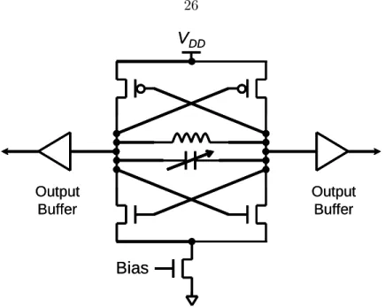
Self-Dividing Oscillators
This can easily be done by driving two identical ILFDs with a pair of differential signals such as using digital dividers, as shown in Fig. It is such a circuit that combines an oscillator with a number of ILFD (M ≥ 2) with injection locking, as shown in Fig. As we discussed earlier, SDO can be used to generate LO signals with low phase noise.
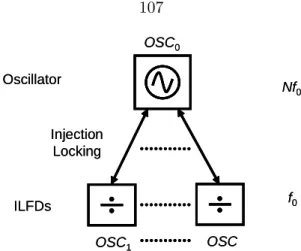
OSC1
2f0 or quadrature signals with ultra-low phase noise at f0 or both (which is especially useful in frequency synthesis). Due to the injection-locked nature and higher power efficiency, SDOs can achieve a significant improvement in phase noise compared to conventional LC oscillators. The signals are injected directly into the ILFD resonator (OSC1 and OSC2) and indirectly into the oscillator resonator (OSC0), while the ∇ topology above does the opposite. In this way, OSC0, which oscillates at 2f0 and normally limits the overall phase noise performance of the SDO, can achieve better standalone phase noise because: 1) there is no direct load on its resonator and therefore the Q resonator is not degraded; 2) it can have a larger amplitude of oscillation due to a larger space for direct current.
Injection
- Summary
In this chapter, injection-locked frequency dividers are presented as the alternative solution for high-speed dividers, which have lower power consumption and better noise performance than conventional digital dividers. In addition, a distributed passive network can generate accurate, controllable time delays for high-frequency/high-speed signals. MMIC adaptive transverse filtering using Gilbert cells and is suitable for high-speed light wave systems.