Ultrafast Relaxation Dynamics and Optical Properties of GaAs and GaAs-based Heterostructures
By
Stephanie N. Gilbert Corder Dissertation
Submitted to the Faculty of the Graduate School of Vanderbilt University
in partial fulfillment of the requirements for the degree of
DOCTOR OF PHILOSOPHY in
Interdisciplinary Materials Science December, 2014
Nashville, Tennessee
Approved:
Jimmy Davidson, PhD Richard Haglund, PhD Timothy Hanusa, PhD
Norman Tolk, PhD Kalman Varga, PhD
INTERDISCIPLINARY MATERIALS SCIENCE
Ultrafast Relaxation Dynamics and Optical Properties of GaAs and GaAs-based Heterostructures
Stephanie N. Gilbert Corder
Dissertation under the direction of Professor Norman H. Tolk
Three previously unreported photo-carrier relaxation pathways are presented and discussed in GaAs-based systems. In bulk GaAs, a transient bleach of the spin-split exciton transition 1s→2p± is reported following photo-excitation at low temperatures and is likely caused by final state blocking of the 2p±1 exciton level. The bleach of the 1s→2p−1 transition is delayed with respect to that of the free carriers and 1s→2p+1, suggesting electronic relaxation occurs through two simultaneous mechanisms: elastic scattering between quan- tized conduction band states and spin-dependent relaxation through the 2p±1exciton states.
For ErAs:GaAs composites, the response at short time delays is completely dependent on the occupation of the interface trap state between the ErAs nanoparticles and the GaAs matrix. Occupation of the interface state depends on the photo-carrier energy, carrier den- sity, and trap density. Carrier scattering from the interface state plays a large role in the response as it prevents full relaxation of the system on ultrashort timescales. The compos- ite ErAs:GaAs systems also exhibit an oscillatory response highly suggestive of surface plasmon polaritons at the interface between the semi-metallic ErAs and semiconducting GaAs, which couple to the GaAs phonon modes. The oscillation frequencies are observed to follow the same trend with volume fraction as the static absorption resonance peaks, suggesting different nanoparticle size distributions exist with different ErAs incorporation.
To my mom and grandpa
for their unending support.
ACKNOWLEDGMENTS
I would like to thank several people without whom this project would not have been com- pleted. First and foremost, my advisor Norman Tolk for his vision and support, the Tolk research group members past and present who made this process enjoyable, G. Larry Carr for his mentorship and willingness to work with me, my family and friends for mental sup- port during this process, and finally my husband Chris, whose unceasing questions led me to think deeper about my research than anyone else, even when it was unwillingly so.
I would like to gratefully acknowledge the VINSE core laboratories for access to equip- ment, the NSF IGERT program, the Department of Energy and Army Research Offices for funding.
TABLE OF CONTENTS
Page
DEDICATION . . . ii
ACKNOWLEDGMENTS . . . iii
LIST OF FIGURES . . . ix
LIST OF TABLES . . . x
Chapter 1. INTRODUCTION. . . 1
Interest in Bulk GaAs. . . 2
Interest in ErAs:GaAs Composite Systems . . . 2
Organization . . . 3
2. OPTICAL PROPERTIES OF GALLIUM ARSENIDE . . . 5
Introduction to Optics . . . 5
Macroscopic Form of Maxwell’s Equations... 5
Properties of the Medium... 6
Complex Index of Refraction and Dielectric Constants ... 7
Drude-Lorentz Model of Optical Properties... 12
Band Structure of Solids . . . 14
Metallic vs. Insulating Materials ... 16
Effective Mass... 19
Landau Levels ... 20
Semiconductor Dynamics . . . 22
Optical Excitation of a Crystal Lattice ... 22
Quasiparticles and Quanta in an Excited Crystal Lattice... 23
Carrier Relaxation ... 28
Measuring Dynamic Properties with Pump and Probe Spectroscopy . . . 30
Summary . . . 31
3. MAGNETO-SPECTROSCOPY OF GAAS . . . 32
Introduction . . . 32
Exciton Excitation and Relaxation Dynamics . . . 34
Experimental Setup . . . 38
Static Absorption Spectroscopy of GaAs . . . 39
Photo-Induced Spectroscopy of GaAs ... 41
Time-Resolved Pump and Probe Spectroscopy . . . 46
Differential Transmission of GaAs ... 47
Summary . . . 53
4. RELAXATION PATHWAYS IN ERAS:GAAS SYSTEMS . . . . 54
Introduction . . . 54
State of Research . . . 56
Growth Process... 56
The Bulk ErAs:GaAs Interface Structure ... 57
Electrical Characterization of the Embedded Nanoparticle ErAs:GaAs Interface ... 59
Previous Optical Studies of Superlattice Structures and Related Systems . 59 Single Layer ErAs:GaAs Dynamics . . . 66
Sample Structure and Growth ... 66
Experimental Details ... 67
Results and Discussion . . . 69
Conclusions . . . 78
5. SURFACE PLASMON POLARITONS IN ERAS:GAAS . . . . 80
Motivation . . . 80
State of Research . . . 81
ErAs Absorption Across a Confinement-Induced Bandgap ... 81
ErAs Absorption as a Surface Plasmon Resonance ... 82
Experimental Description . . . 84
Samples Under Investigation ... 85
Static Infrared Absorption... 87
Time-Resolved Optical Measurements ... 89
Summary . . . 93
6. CONCLUDING REMARKS . . . 95
7. APPENDIX . . . 98
Excitonic Calculations . . . 98
Carriers per Island Calculation . . . 98
Simulation Code for the ErAs:GaAs Potential Barrier Dynamics. . . 99 Phonon Frequencies . . . 108
BIBLIOGRAPHY . . . 109
LIST OF FIGURES
Figure 2.1 The Electromagnetic Wave . . . 6
Figure 2.2 Reflection and Transmission at an Interface . . . 10
Figure 2.3 Schematic Diagram of the Atomic States of a Covalent Crystal Forming Energy Bands . . . 15
Figure 2.4 Electron Occupancy of States at Room Temperature . . . 17
Figure 2.5 The GaAs Crystal Structure . . . 18
Figure 2.6 The GaAs Band Structure . . . 19
Figure 2.7 Landau Level Structure at the Band Gap . . . 21
Figure 2.8 Direct Band Gap and Exciton Structure. . . 25
Figure 2.9 Bandfilling Effects . . . 27
Figure 2.10 Basic Recombination Processes in Semiconductors . . . 30
Figure 3.1 Heavy Hole Exciton Absorption Peak in a Quantum Well Structure . . . 35
Figure 3.2 Non-Resonant Exciton Formation . . . 36
Figure 3.3 Theoretical Contributions to Differential Absorption Spectra. . . 37
Figure 3.4 NSLS Experimental Design. . . 39
Figure 3.5 Temperature Dependence of the Exciton Population. . . 40
Figure 3.6 Field Dependence of the GaAs Absorption Edge at 20 K. . . 41
Figure 3.7 Photo-induced Absorption Spectra of GaAs at 50 K as a Function of Field . . . 42
Figure 3.8 Photo-induced Absorption Spectra of GaAs at 5 K as a Function of Field . . . 43
Figure 3.9 Static Absorption Spectra and Model of Transitions . . . 44
Figure 3.10 Photo-induced Spin-dependent Exciton Transitions . . . 45
Figure 3.11 Photo-induced Absorption Spectra of GaAs at 5 T and 5 K as a Function of Excitation Wavelength . . . 47
Figure 3.12 Photo-induced Absorption of GaAs Oscillator Strength and Mode Width at 5 K as a Function of Photo-excitation Energy . . . 48
Figure 3.13 Formation of the Differential Transmission Response at 5 T, 5 K and 795 nm . . . 49
Figure 3.14 Decay of the Differential Transmission Response at 5 T, 5 K and 795
nm . . . 50
Figure 3.15 Effective Mass Comparison for Different Applied Magnetic Fields at 784 nm and 5 K . . . 51
Figure 3.16 Effective Mass Comparison for Different Excitation Wavelengths at 5 K . . . 52
Figure 3.17 Oscillator Transition Strengths at 5 T, 5 K, and 784 nm . . . 53
Figure 4.1 ErAs:GaAs Deposition Dependence and Current Density . . . 57
Figure 4.2 Structural Model of the ErAs:GaAs (001) Interface . . . 58
Figure 4.3 High-angle Annular Dark-field Images TEM of the ErAs/GaAs Interfaces . . . 60
Figure 4.4 Average Differential Conductance for ErAs Nanoparticles and GaAs Matrix. . . 61
Figure 4.5 Optical-pump THz-probe of GaAs Reference . . . 62
Figure 4.6 ErAs:GaAs Superlattice Optical Pump-THz Probe Response. . . 62
Figure 4.7 ErAs:GaAs Superlattice Transient Decay as a Function of Superlattice PeriodL . . . 63
Figure 4.8 ErSb:GaSb Superlattice Transient Decay as a Function of Superlattice Growth Parameters. . . 65
Figure 4.9 ErSb:GaSb Superlattice Growth Parameters . . . 66
Figure 4.10 Absorption and Sample Structure of the ErAsx:GaAs1−xComposite System.. . . 68
Figure 4.11 Spectral Response of ErAsx:GaAs1−xat 1.38 eV. . . 71
Figure 4.12 Spectral Response of ErAsx:GaAs1−xat 1.46 eV. . . 73
Figure 4.13 Spectral Response of ErAsx:GaAs1−xat 1.55 eV. . . 76
Figure 5.1 Absorption Spectra for 0.5-4.5% ErAs . . . 82
Figure 5.2 Transmission and Absorption for ErAs/GaAs Superlattices . . . 83
Figure 5.3 Normalized Transmission for Three ErAs:GaAs Samples at Room Temperature . . . 84
Figure 5.4 ErAsx:GaAs1−xComposite Absorption Data . . . 86
Figure 5.5 ErAsx:GaAs1−xComposite Absorption Change . . . 87
Figure 5.6 ErAsx:GaAs1−xComposite Absorption in the Mid-Infrared . . . 88
Figure 5.7 Oscillatory Response of ErAsx:GaAs1−xComposites at 1.55 eV . . . 89 Figure 5.8 Oscillation Frequencies of ErAsx:GaAs1−xComposites at 1.55 eV . . . . 90 Figure 5.9 Oscillatory Response of 10% ErAsx:GaAs1−x at 1.38 eV . . . 92 Figure 5.10 Frequency of 10% ErAsx:GaAs1−xat 1.38 eV . . . 93 Figure 5.11 Polarization Dependence of the Oscillatory Response Below the
Bandgap . . . 94 Figure 7.1 GaAs Characteristic Timescales for Excitation at 1.46 and 1.55 eV . . . . 107
LIST OF TABLES
Table 2.1 Quanta of Crystal Lattice Excitations . . . 23 Table 2.2 Photo-excited Semiconductor Relaxation Regimes. . . 29 Table 3.1 Energy in Different Units for Comparison. . . 39 Table 5.1 Average Observed Oscillation Frequencies Compared to Phonon
Frequency at 1.55 eV . . . 91 Table 7.1 Experimental Values of the Index of Refraction and Expected
Phonon Frequencies at 1.55 eV . . . 108
CHAPTER 1
INTRODUCTION
There are two possible outcomes:
if the result confirms the hypothesis, then you’ve made a measurement.
If the result is contrary to the hypothesis, then you’ve made a discovery.
Enrico Fermi
Photo-excitation in condensed matter systems results in the creation of complex many-body states arising from the interaction of quasiparticles and quanta of the excited system. The evolution of these many-body states is of fundamental interest as knowledge of such behav- iors could motivate the creation of devices. The work presented in this dissertation is based on understanding the relaxation dynamics of gallium arsenide (GaAs), the archetypal III-V compound semiconductor, following photo-excitation. Gallium arsenide has long been a material of great interest in semiconductor research as a result of its direct band gap and optical accessibility with femtosecond (fs) Ti:Sapphire laser systems. Due to its relative popularity, many have assumed there is no work remaining in the study of GaAs and have moved on to less familiar semiconductors and composite systems. As will be seen in the subsequent chapters, many questions remain about the general GaAs relaxation process and its time-evolution.
The techniques used in this work are static and time-resolved optical spectroscopy. These optical methods provide fundamental information about nonlinear properties, non-equilibrium dynamics, many-body effects, state occupation and transport properties of semiconductors.
Photo-excitation generates carrier populations with non-equilibrium temperature distribu- tions, and optical spectroscopy provides the best means of characterizing population distri- butions as well as determining their relaxation dynamics [1].
Relaxation dynamics in semiconductors occur in different temporal regimes. As a result, different optical techniques are required to characterize the full relaxation process. For GaAs optically excited at 300 K, carriers undergo rapid energy and momentum redistri- bution within the first few picoseconds (ps). The system thermalizes in nanoseconds (ns), with full equilibrium occurring in tens of ns. These time scales are significantly slower when the system is held at cryogenic temperatures.
Interest in Bulk GaAs
The characterization of the relaxation dynamics of intrinsic GaAs provides a way to inves- tigate many-body effects in a compound semiconductor. Effects such as band-gap renor- malization, carrier interactions, alteration of exciton binding energies, energy level broad- ening, bleaching, phase space filling, alteration of matrix elements, and non-equilibrium occupation of states all depend on the photo-excited carrier density and the system being investigated.
Interest in ErAs:GaAs Composite Systems
Manipulation of the GaAs relaxation process can be achieved through the incorporation of nanoparticulates co-deposited with GaAs during the molecular beam expitaxy (MBE) growth process. Metal-semiconductor composites have hybrid electronic, dielectric and optical properties that may be controlled by manipulating the amount of metal in the semi- conductor [2], enabling the engineering of materials for specific uses. The incorporation of erbium (Er) in the GaAs growth process yields composite ErAs:GaAs systems. These
composite systems offer improved detection efficiency and performance as compared to other common detection materials like low temperature (LT) grown GaAs [3] while nearly doubling the efficiency of GaAs-based multi-junction solar cells [4]. The system is also a major contender for the development of compact terahertz (THz) generators and detectors capable of being excited with commercially available lasers at 800 nm [5]. Composites of ErAs:GaAs may be grown at temperatures above 450◦ C, resulting in higher crystal qual- ity and improved transport characteristics like carrier mobility in comparison to LT GaAs which is grown around 250◦C [6, 7]. The ErAs nanoparticles have intrinsic carrier trap- ping times below 190 fs which can be tuned over two orders of magnitude by changing the growth parameters [8].
In addition to the trapping behavior, the inclusion of metallic particles in semiconductors results in infrared resonances [2]. The incident light field displaces the metallic electrons in the nanoparticles, causing accumulation or depletion of charge at the edges and resulting in a net restoring force on the electrons. The electron oscillations can have large amplitudes under resonant excitation, resulting in localized surface plasmons [9].
Organization
The subsequent chapters are organized as follows: Chapter 2 contains an overview of the physical concepts used in this work, including a general description of GaAs optical and structural properties. Relevant semiconductor concepts relating to the absorption of pho- tons by a direct bandgap semiconductor and relaxation pathways are introduced. The be- havior of an optically excited semiconductor in an applied magnetic field and excitation quanta in a condensed matter system will also be discussed.
Chapter 3 details the characterization of the static and transient absorption of GaAs sub- jected to low temperatures and high magnetic fields in the far-infrared (FIR) spectral region.
The data provide evidence for a previously unreported relaxation pathway in GaAs through Auger-like scattering of Landau-quantized electrons into exciton states.
Chapters 4 and 5 will detail studies of ErAs:GaAs composite systems. The composites are characterized using static and time-resolved optical techniques in the near infrared (NIR).
Chapter 4 shows the interface between the embedded semi-metallic ErAs and the GaAs host behaves as a Schottky barrier. Carrier trapping and scattering are observed to de- pend highly on the occupation of the interface states. Chapter 5 explores the response of the ErAs:GaAs system at longer time delays following photo-excitation. The results sug- gest surface plasmon polaritons generated when the ErAs nanoparticles are photo-excited couple strongly to GaAs lattice excitations, creating a long-lived oscillating response and enhancing absorption below the GaAs conduction band edge.
Chapter 6 summarizes the results of this work, including detailing the three previously un- reported dynamic pathways observed in GaAs-based systems and their potential impact on device engineering.
The appendix contains example calculations referenced in the text, as well as the simula- tion code used in Chapter 4 to show the composite ErAs:GaAs system dynamics can be represented by a simple 3 level system.
CHAPTER 2
OPTICAL PROPERTIES OF GALLIUM ARSENIDE
Never memorize something that you can look up.
Albert Einstein
Properties of material systems must be understood in order for technical applications to be realized. The optical response of solid materials can provide valuable information about the nature of the system, like the electronic structure, transport properties, bond strength, defect structure, many-body effects, and relaxation dynamics all. The following introduces the interaction light with semiconductors, with a specific focus on GaAs.
Introduction to Optics
The interaction of light and matter can be described at the most fundamental level using Maxwell’s equations. Optical wavelengths are thousands of times larger than the size of an atom. Therefore, within a unit wavelength the atoms present in a solid can be treated as continuous when averaged over the microscopic spatial fluctuations [11, 12]. As a result, the semi-classical macroscopic form of Maxwell’s equations can be used to determine the response of a condensed matter system to an optical field.
Macroscopic Form of Maxwell’s Equations
Maxwell’s equations relate the most basic quantities to uniquely determine the field vectors from a distribution of currents and charges. The electric field vectorE, magnetic induction
Figure 2.1An electromagnetic wave propagating in thezdirection where the electric field is represented in blue and the magnetic field in red, from [10].
B, magnetic field vectorH, electric displacementD, and electric current density Jmay be written in macroscopic form as:
∇·D=4π ρ (2.1)
∇×E=−1 c
∂B
∂t (2.2)
∇·B=0 (2.3)
∇×H= 1 c
∂D
∂t +4π
c J (2.4)
wherecis the speed of light in a vacuum andρ is the electric charge density.
Properties of the Medium
Maxwell’s relations are supplemented by materials equations which describe the response of a system to the electromagnetic field. For a harmonic electromagnetic field and a mate- rial system at rest, the linear materials equations are
j=σE (2.5)
D=εE=ε0E+P (2.6)
B=µH=µ0H+M (2.7)
whereσ is the specific conductivity,ε is the dielectric constant,Pis the polarization,µ is the magnetic permeability, andMis the magnetization of the medium [13].
The polarization of the mediumPinduced by the electromagnetic field can be expressed in terms of the electric field components as a tensor relation
P=ε0χEE (2.8)
whereχE is the electric susceptibility tensor. Likewise, the magnetic susceptibly tensorχM may be described by
M=µ0χMH (2.9)
Conductors are materials in which σ is non-zero. Insulators or dielectrics have negligi- bly small σ values, and their electric and magnetic properties may be completely deter- mined by εr and µr. For nonmagnetic materials (µr=1), the dielectric function connects the displacement field of the medium with the electric field of the light and is the basis for characterizing the optical response of semiconductors.
Complex Index of Refraction and Dielectric Constants
The most general phenomena describing the interaction of solid materials with light can be classified into three groups: transmission, reflection, and propagation. During propagation, the light may be refracted (waves travel slower than in free space, bending the light rays as described by Snell’s law), absorbed (the beam is attenuated), and scattered (light interacts with the medium, causing it to change direction and possibly frequency, also attenuating the beam) [14].
Dynamic properties may be investigated using the reflection and refraction of light at a planar interface between dielectrics through changes in intensity, phase, and polarization of the electromagnetic radiation [12]. Reflection at the surface of the material is determined by the coefficient of reflectivity,R, and is defined as the ratio of the reflected power to the power incident on the surface. Similarly, the transmission is determined by the coefficient of transmissivity, T, which is the ratio of the transmitted power to the incident power. In the absence of scattering,
R+T+A=1 (2.10)
where the absorption,A, will be defined below.
The absorption coefficient α is used to quantify the absorption of light in a medium by defining the fraction of power absorbed per unit length of the material according to Beer’s Law:
I(z) =I0e−αz (2.11)
whereI0is the optical intensity atz=0 for a beam propagating in thezdirection.
In a transparent medium, the propagation of an incident beam is described by the refractive indexn, wherenis defined as the ratio of the velocity of light in free space,c, to the velocity of light in the mediumv:
n= 1
√µ ε =c
v (2.12)
wherenis dependent on the frequency of the incident light beam, producing an effect called dispersion.
The absorption and refractive index are incorporated into a quantity called the complex
index of refraction given by
˜
n=n+iκ (2.13)
whereκ is the imaginary term called the extinction coefficient and is related to the absorp- tion by
α = 4π κ
λ (2.14)
whereλ is the wavelength of light in free space.
The relative dielectric functionεr (or relative permittivity) is related to the vacuum dielec- tric constant through
εr(ω) = ε(ω)
ε0 =ε1+iε2 (2.15)
whereε(ω)is the frequency dependent absolute dielectric function of the material.
εr is related to the complex index of refraction ˜n and the two quantities are commonly used to describe optical properties of dielectric materials. For nonmagnetic matter, the two quantities are related to one another by the following equations [14]
ε1=n2−κ2 (2.16)
ε2=2nκ (2.17)
n= v u u t
q
ε12+ε22+ε1
2 (2.18)
κ= v u u t
q
ε12+ε22−ε1
2 (2.19)
Both sets of optical constants are equally valid but have different utility in understanding matter:nandκare related to the phase velocity and attenuation of plane waves in materials
whileε1andε2are useful when considering sub-wavelength optical effects.
n1 n2 Ei
Er
Et
!i
!r
!t
Figure 2.2Reflection and transmission at an interface.
The reflectivity of a dielectric depends on the complex index of refraction. Reflection and transmission of light at an interface are a function of the angle of the light incident on the material surface and also the light polarization [15]. The incident and reflected anglesθi,r
are defined relative to the material surface normal. The reflection and transmission can be resolved into perpendicular components: R=r2p+rs2 andT =t2p+ts2. For polarization in the plane of incidence (ppolarization), the reflection at an interface is given by
rp= Er Ei =
n22cosθi−n1 q
n22−n21sin2θi
n22cosθi+n1 q
n22−n21sin2θi
(2.20)
where Er (Ei) is the reflected (incident) electric field and θr has been eliminated using Snell’s law. n1is the index of refraction of the medium in which the light is propagating (usually air or vacuum) whilen2is the index of refraction of the material under investigation (see Figure 2.2).
The transmission is given by
tp= Et
Ei = 2n1n2cosθi n22cosθi+n1
q
n22−n21sin2θi
(2.21)
whereEt is the transmitted electric field.
For polarization perpendicular to the plane of incidence (spolarization), the reflection and transmission are, respectively;
rs= Er Ei =
n1cosθi− q
n22−n21sin2θi n1cosθi+
q
n22−n21sin2θi
(2.22)
ts= Et
Ei = 2n1cosθi n1cosθi+
q
n22−n21sin2θi
(2.23)
For normal incidence, (θi=0), the reflection and transmission of both polarizations reduce to
rp,s= Er
Ei = n2−n1
n2+n1 (2.24)
tp,s=Et
Ei = 2n1
n1+n2 (2.25)
The rp,s and tp,s constitute the Fresnel coefficients of reflection and transmission where in the absence of absorption rp+tp =1 and rs+ts =1. It can clearly be seen that the observed reflection or transmission from a surface is highly dependent on the incident angle and polarization of the light, as well as the material properties described by the index of refraction. To further investigate the response of a system to an applied electromagnetic field, the material response will be modeled as a microscopic harmonic oscillator.
Drude-Lorentz Model of Optical Properties
The classical Lorentz theory of optical properties makes the assumption that electrons and ions in a material can be modeled as simple harmonic oscillators subjected to a driving force by means of an applied electromagnetic field. The equation of motion for an electric charge -eof massmis given by
m[¨x+γ˙x+ω02x] =−eE(x,t) (2.26)
where γ is the damping coefficient and ω0 is the resonance frequency [12]. For a field varying harmonically (e−iωt) in time with frequencyω, the dipole momentpof one electron is
p=−ex= e2 m
E
(ω02−ω2−iω γ) (2.27)
The material response is the sum of individual dipoles, so for N molecules per unit volume with fjelectrons per molecule, binding frequenciesωj, and damping constantsγj;
∑
j
pj=−Nex= Ne2E
m
∑
j
fj
(ω2j −ω2−iω γj) (2.28) Given equation 2.27 and the dielectric functionεr(ω)= 1+χ, equation 2.28 can be written as
εr(ω) =1+Ne2 ε0m
∑
j
fj
(ω2j−ω2−iω γj) (2.29) where the fjare referred to as oscillator strengths [12].
Low Frequency Response of the Dielectric Function: Optical Conductivity
If some fraction of the electrons per molecule are unbound (ω0= 0), asω approaches zero the dielectric function can be written
ε(ω) =εbg(ω) +i Ne2f0
mω(γ0−iω) (2.30)
whereεbg is the background dipole contribution from the free electrons [12]. The conduc- tivityσ may be written as
σ = f0Ne2
m(γ0−iω) (2.31)
when the properties of the medium arise from only the dielectric function [12]. Equation 2.31 is the Drude conductivity for the medium if the number free electrons per unit volume in the medium is f0N.
High Frequency Response of the Dielectric Function: Plasma Frequency
For high frequencies whereω γ0, the dielectric function in equation 2.30 can be approx- imated as
ε(ω) =εbg(ω)−ε0 ωp2
ω2 (2.32)
whereωpis defined as the the plasma frequency of the conduction electronsωp2=Ne2/m∗ε0 and includes binding effects through the effective mass termm∗(see below) [12].
In small metal nanoparticles, the optical properties are dominated by surface plasmon res- onance effects [16]. The polarizability of a sphere is given by
P= χeε0E
1+χe/3 (2.33)
Assuming the carriers in the nanoparticle behave as a free electron gas, the susceptibility
may be written as:
χe(ω) =− Ne2
m∗ε0ω2. (2.34)
Combining the previous two equations, one sees
P(ω) = ε0E
1−Ne2/3m∗ε0ω2 = ε0E
1−ω2p/3ω2 (2.35)
where ωp is the plasma frequency of the bulk metal. The polarization equation diverges for frequency values of ωsp=ωp/√
3 where ωsp is the surface plasmon frequency of the metal sphere [16].
Band Structure of Solids
The close proximity of atoms in a solid results in the interatomic separation distance being approximately the same size as the atom, producing overlap of the orbitals and strong inter-atomic interactions. This creates a broadening of the discrete atomic levels into bands which form a continuum of states [14].
Electrons in a crystal are arranged in energy bands separated by forbidden regions, or band gaps, in which no electron orbitals exist. The bands form as a result of the interaction be- tween the lattice ions and electron wavefunctions [16]. Bragg reflection of electron waves in the crystal give rise to energy gaps, as traveling wave solutions to the Schr¨odinger equa- tion do not exist at points satisfying the Bragg condition [16].
Band theory arises from the single electron approximation, wherein an electron is assumed to be subject to the effective (average) potential field of fixed lattice ions, inner shell elec- trons, and other valence electrons [11, 17]. For perfect crystals, the potential energy of the crystalV(r)has the periodicity of the lattice. Solutions of the Schr¨odinger equation
Interparticle Separation molecule atom
crystal
s p p antibonding
s antibonding
p bonding
s bonding conduction band
valence band
Figure 2.3Schematic diagram of the atomic states of GaAs. As the interparticle separation decreases, thesandpstates of the atoms hybridize, forming occupied bonding and unoc- cupied antibonding molecular states. The bonding and antibonding states evolve into the valence and conduction bands as the interparticle spacing decreases further.
¯ h2
2m∇2ψ+ [E−V(r)]ψ=0 (2.36) are Bloch functions of the form
ψ(k,r) =uk(r)exp(ik·r) (2.37)
whereuk(r)has the periodicity of the lattice,kis the crystal momentum, andris the radial direction [11]. This indicates there are eigen-energiesE wherekis real and electron wave functions exist; conversely, there are energy ranges where k is imaginary and no energy states exist [17]. The eigenstates wherekis real are referred to as the energy bands of the solid and the imaginary states are the forbidden states or energy gaps. In this way, the band structure of the solid is a direct result of the periodicity of the lattice.
For free electrons, eigen-energies can be written as
E = p2
2m = h¯2k2
2m (2.38)
and the energy bands of a material are then plotted in terms of energy vs.k-space direction.
For real crystals, spin-orbit coupling, crystal field lattice splitting, and other effects lift the degeneracies of some points in thek-space plot.
Taking into account the two spin orientations of electrons, there are2Nindependent orbitals in each energy band, whereN is the number of atoms in the primitive cell. Materials with fully occupied bands are insulators provided the filled bands are separated by an energy gap from the next higher band as in Figure 2.4. For crystals with even numbers of valence electrons per primitive cell, but with no energy gap between levels, two partially filled bands may exist and therefore the crystal is a metal.
Metallic vs. Insulating Materials
As previously stated, the occupancy of the highest band containing electrons determines whether a material is metallic or insulating. If the band is partially full, electrons may take part in conduction. For metals, the structure and number of valence electrons per atom produces occupied and unoccupied bands with no energy gap between them [15]. If the highest occupied band is completely full, no electrons are available for conduction and the material is an insulator. The band gap is the energy difference between the lowest point of the conduction band (conduction band edge) and the highest point of the valence band (valence band edge).
The highest occupied energy level is called the Fermi level and is defined in metals such that all the states below are occupied and states above are unoccupied. The dielectric response of a metal is due to intraband transitions: where an electron is excited from an occupied
Energy'
Insulator' Semiconductor' Semimetal' Metal' VB'
CB' Eg'
Figure 2.4Electron occupancy of states at room temperature. Dark blue shading represents fully occupied bands and light blue shading indicates partially filled bands. The conduction band (CB) is separated in energy from the valence band (VB) by the energy gap (Eg).
The availability of states and electron number determine whether a material is insulating, semiconducting, semimetallic or metallic.
to unoccupied state within the same band, changing crystal momentumk and requiring a quantized lattice vibration or impurity to conserve momentum [15].
An intrinsic (undoped) semiconductor is characterized by a bandgap separating an occu- pied valence band and empty conduction band at low temperatures [1]. The conductivity of intrinsic semiconductors increases with temperature: an electron in the highest occupied (valence) band is thermally excited to the lowest empty (conduction) band [17]. The energy difference required to excite the electron from the valence to conduction band is called the intrinsic band gap. The vacancy left in the valence band by the excited electron is called a hole, and behaves like a positively charged electron. As the temperature of the intrinsic semiconductor increases, the energy gap between the highest occupied valence band and lowest unoccupied conduction band decreases.
If no momentum change (∆k=0) is required to photo-excite a carrier from the valence band maximum to the conduction band minimum, the semiconductor has a direct band gap. If a momentum change is required, photo-excitation must involve quantized lattice
vibrations or impurity states. In this case, the material has an indirect band gap.
Band Structure of GaAs
The GaAs lattice consists of two interpenetrating face-centered cubic lattices as can be seen in Figure 2.5. The Zinc Sulfide structure consists of four valence electrons per atom and eight atoms per unit cell [15]. Each electron can be in either a bonding or antibonding state, resulting in 16 states per value ofkspace, or eight bands. In the ground state, GaAs has four completely full valence or bonding bands and the top four conduction/antibonding states are empty. The gap between the bonding and antibonding states makes GaAs a semiconductor [15].
Figure 2.5Crystal Structure of GaAs: Zinc Blende or two interpenetrating FCC sublattices.
The Ga ions are indicated by red balls while the As ions are represented as purple balls.
The tetrahedral bonding structure is evident. From [18].
Bulk GaAs has cubic symmetry; therefore, the conduction band at the zone center has s or- bital character with two-fold spin degeneracy. The valence band has p orbital character and
Figure 2.6The GaAs band structure at 300K. The direct bandgap Egis at 1.42 eV. The EL transition is at 1.71 eV and the EX is at 1.90 eV. The split off hole band ESO is 0.34 eV below the top of the valence band. Adapted from [19].
the top of the valence band is four fold degenerateJ=3/2 due to the spin-orbit interaction.
This results in heavy hole (HH) and light hole (LH) bands, each two-fold degenerate due to uniaxial stress [1]. The room temperature band structure of GaAs can be seen in Figure 2.6.
Motion of the electrons and holes within an energy band is determined by the energy- momentum dispersion in the material. In a crystal, the electrons are not really free, and equation 2.38 is modified by the lattice ion potential [14].
Effective Mass
The energy bands in a semiconductor or insulator are parabolic for small values of kand have dispersions given by
Ec=Eg+h¯2k2
2m∗e (2.39)
Ev=−h¯2k2
2m∗h (2.40)
whereEc,vis the energy of the conduction or valence band, andm∗e,his the electron or hole effective mass, respectively. The effective massm∗defines the band curvature
1 m∗ = 1
¯ h2
∂2E
∂k2 (2.41)
The effective mass is thus a measure of the curvature of the energy band ink-space. m∗ will be close tom0 near the bottom of the parabolic conduction band. If the energy band has littlekdependence,m∗is very large [16].
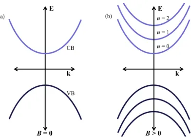
Landau Levels
When a strong magnetic field is applied to a semiconductor, it causes the conduction elec- trons to move in circular orbits around the field at a frequency ωc = meB
0 known as the cyclotron frequency. The energy and radius of the electron orbits have discrete values. The quantized energies, known as Landau levels, followEn= (n+1)¯hωc wheren=0,1,2, ...
[14]. Electrons in a magnetic field move ink-space on a surface of constant energy, normal toB[16].
For a direct gap semiconductor with the magnetic fieldBapplied in the ˆzdirection and the sample plane in ˆx- ˆy, the motion of the electrons in the conduction band will be quantized in the ˆx- ˆy plane with free motion in the ˆz. For this reason, it can be considered a two- dimensional system. Carriers within the Landau levels have energies given by
En(kz) = (n+1 2)ehB¯
m∗ +h¯2k2z
2m∗ (2.42)
wherem∗ is the effective mass of the appropriate carrier andnis the index of the Landau level as can be seen in Figure 2.7. The first term describes the quantized motion in the ˆx- ˆy plane while the second is the motion in the ˆzdirection.
(a) (b)
E
k
E
k
B = 0 B > 0
n = 0 n = 1 n = 2
CB
VB
Figure 2.7 Effect of applied magnetic field on the band structure. a) Band structure in the absence of an applied magnetic field where CB indicates the conduction band and VB the valence band. b) Landau level structure at the bandgap in the presence of an applied magnetic field showing quantized levels in both the conduction and valence bands.
To determine the transition energy between different Landau levels, it is useful to redefine the position of zero energy, whereE=0 is defined as the top of the valence band. Interband transitions require both an electron in the initial state and an available state (hole) in the final state. Equation 2.42 can therefore be separated into the electron and hole components:
Een(kz) =Eg+ (n+1 2)e¯hB
m∗e +h¯2k2z
2m∗e (2.43)
Ehn(kz) =−(n+1 2)e¯hB
m∗h +h¯2k2z
2m∗h (2.44)
The selection rule for interband transitions between Landau levels is ∆n=0. Therefore, the interband transition energy is given by
hω¯ =Een(kz)−Ehn(kz) =Eg+ (n+1 2)e¯hB
µ +h¯2k2z
2µ (2.45)
where µ1= m1∗ e+m1∗
h is the reduced mass of the electron-hole pair [14]. The selection rules
indicate the electron and hole have the samenvalue, as well askz≈0 due to the negligible momentum of the photon. This results in equally spaced absorption spectra peaks with energies given by
ELn=Eg+ (n+1 2)ehB¯
µ (2.46)
for positive integer values ofn. The absorption edge shifts to higher energy in a magnetic field according toe¯2µhB. The electron effective mass can be determined from the transmission response and the width of the Landau levels is caused by carrier scattering [14].
Semiconductor Dynamics
Optical excitation is the main method used in this work to perturb a material system from its steady state configuration. Optical excitation results in the absorption of a photon by a crystal lattice. Different methods of absorption exist, depending on the photon energy and available states.
Optical Excitation of a Crystal Lattice
When light of sufficient energy is incident on a material, it causes transitions of electrons from states below the Fermi level to states above [11]. Light incident on metallic systems produces intraband absorption, in which a carrier is excited to a higher energy within the same band. For intrinsic semiconductors and insulators, the band gap of the material deter- mines the minimum energy at which photons are absorbed. This is called the fundamental absorption edge and carriers in the valence band are excited into the conduction band in a process termed interband absorption. Interband absorption results in the creation of an electron-hole pair, with the electron excited to the conduction band and the hole in the valence band [14].
Quasiparticles and Quanta in an Excited Crystal Lattice
Given the right conditions, excitation of a crystal may result in quantized energy states.
A few examples relevant to this work are presented below and in Table 3.1; including quantized electron-hole pairs, lattice vibrations and oscillating electrons.
Name Field Characteristic Properties Characteristic Modes Phonons Elastic Wave Lattice Vibrations Optic and Acoustic Plasmons Electron Wave Free Electrons and Photons Geometric
Excitons Polarization Wave Electron-Hole Pairs Discrete Orbitals Polaron Electron-Elastic Wave Electrons and Phonons Dispersive
Table 2.1Quanta of Crystal Lattice Excitations.
Excitons
The mutual Coulomb attraction of a photo-excited electron and hole can lead to the forma- tion of a bound pair, known as an exciton. Excitons form a hydrogenic system of bound states converging with the conduction band and give rise to an increase in absorption near the band edge [1]. In general, there are two types of excitons: free excitons (Wannier- Mott) and tightly bound (Frenkel) excitons [14]. This work will focus on free excitons, which have a large binding radius and tend to be delocalized states able to move through the crystal. Excitons are stable only if the binding energy is sufficiently large to prevent disruption from thermal effects, such as lattice vibrations. The room temperature thermal energy iskBT ≈25 meV and the binding energy of excitons are on the order of a few meV;
therefore, excitons are generally observed at cryogenic temperatures [14].
The binding energy of an excitonEXcan be determined using the Bohr model with a relative dielectric constant and the reduced mass of the electron-hole pair. The energy of the nth
(for n=1,2,...) level relative to ionization limit is given by
EX(n) =− µRH
m0εr2n2 =−RX
n2 (2.47)
where RH is the Rydberg constant 13.6 eV of the hydrogen atom andRX is the Rydberg constant of the exciton. The radius of the exciton is
rX n= mεrn2aH
µ =n2aX (2.48)
whereaH is the Bohr radius of the hydrogen atom 5.29×10⁻¹¹ m and aX is the exciton radius. From the previous equations, it can be seen that the exciton ground state withn=1 has the largest binding energy and smallest radius. Typical values for GaAs giveRX =4.2 meV andaX =13 nm, where the electron effective mass is 0.067m0andεr =12.8 (static dielectric constant values are used since the binding energies are in the far-infrared spectral region) [14].
Exciton energy from a direct transition (k=0) is the energy required to produce a free electron hole pairEgminus the Coulomb binding energy:
EX n=Eg−RX
n2 (2.49)
implying the formation of exciton states is energetically favorable compared to free elec- tron hole pairs as the total energy is lower (see Figure 2.8). Excitons are observed in the spectra of very pure samples as impurities produce free carriers which screen the Coulomb interaction and reduce the binding energy, as well as generating local electric fields which ionize the excitons.
In addition to thermal instabilities, if the density of excitons is increased sufficiently or
!"#$%&'"#()*#$
+,-&'.-(/*00(/1-
2*3-#&-()*#$
+,-&'.-(/*00(/14 +5&67"#(87*7-0
+#-9:;(<*=(+:
+5&67"#(
>6#$6#:(
-#-9:;
Figure 2.8 Direct band gap and exciton structure, where the lowest exciton level is the ground state and the energy difference between the exciton ground state and the conduction band edge is the exciton binding energy.
free carriers are injected, the Coulomb attraction binding the exciton is screened. In such a situation, thek≈0 electron and hole states are filled, causing a decrease in the observed absorption (bleaching) with increasing laser intensity [14, 20]. The bound states becomes unstable and break up into free electron-hole pairs [20].
Excitons are perturbed by the application of electric and magnetic fields. The strength of the perturbation from magnetic fields is proportional to the exciton cyclotron resonance energy ¯hωc
¯
hωc=h¯eB
µ (2.50)
similar to free electrons except for the reduced electron-hole effective massµ [14].
Phonons
The periodicity of the crystalline lattice in GaAs allows the formation of phonons, or quan- tized vibrations of lattice ions, with resonant frequencies in the infrared [14, 16]. Both acoustic and optical modes are possible as GaAs has eight atoms per unit cell [1]. The
electric field of the incident light can drive resonant oscillations of charged lattice ions to produce transverse optic phonons (TO). Longitudinal optic (LO) modes displace ions per- pendicular to the applied field and thus do not interact with incident light [14].
Acoustic phonon modes require a non-zero wave vector to be created and thus are not directly generated from the incident light. Instead, optical phonons decay into acous- tic phonons which are capable of traveling and scattering within the crystal. Acoustic modes are classified as longitudinal or transverse with different characteristic velocities [1]. Phonons play a large role in the relaxation of semiconductors as they act as an energy and momentum exchange mechanism between excited carriers and the crystal lattice.
Polarons
A polaron is the coupling of an electron and phonon; a local displacement of the crystal lattice immediately surrounding an electron. The distortion of the lattice follows the elec- tron as it travels through the crystal. The polaron mass is larger than the unexcited lattice mass because the electron and lattice distortion move together. The deviation in mass can be measured through the cyclotron resonance frequency.
Surface Plasmons
A quantized oscillation of the free electron gas with respect to the positive lattice ions is called a plasmon. The displacement of the oscillations is in the direction of the electric field [14]. Using the Drude model, the relative dielectric function of a metal nanoparticle may be written as
εs=εB− ωp2
ω2+iω γ (2.51)
whereεB is the real background dielectric constant,ω is the optical frequency, ωp is the plasma frequency, = (1/τ)is the carrier scattering frequency and is the scattering time.
Energy'
VB' CB'
E
g' Excita0on'
Energy'
Figure 2.9Bandfilling effects at room temperature. The conduction band (CB) is separated in energy from the valence band (VB) by the energy gap (Eg). The excitation energy of the light is greater than the bandgap energy, exciting electrons into the conduction band until no more states are available and the exciting light is transmitted.
Resonant Absorption Non-linearities
When large numbers of electrons are photo-excited in a semiconductor with an energy greater than the bandgap, electrons fill the states at the bottom of the conduction band and holes fill the top of the valence band as can be seen in the schematic shown in Figure 2.9.
The exclusion principle holds for interband optical transitions, requiring the final state be unoccupied for an electron to absorb a photon. As the excitation source intensity is in- creased, the absorption gradually saturates as the available bands fill with photo-carriers in an effect called the band-filling nonlinearity [14]. If a carrier of the same type already exists in the final state, the transition is blocked and the effect is referred to as Pauli block- ing or phase space filling. For high excitation densities, Pauli blocking prevents electrons from being excited as there are no available final states. This causes a blockage of further absorption of the excitation light in an effect called saturable absorption. An increase in
transmission resulting from the blockage of further absorption is termed bleaching of the absorption resonance.
Carrier Relaxation
The absorption of light in a semiconductor can create an electron hole pair with excess energy above the fundamental bandgap value. The initial step towards thermal equilibrium involves electrons and holes scattering out of the optically coupled valence and conduction band states [20]. Quasi-thermal energy distributions are established by carrier-carrier and carrier-phonon scattering. Recombination of the excited electrons and holes occurs by ra- diative (photon emission) and non-radiative (trapping and energy transfer/Auger) methods.
Carrier relaxation can be classified into four regimes with overlapping timescales: coher- ent, non-thermal, hot carrier, and isothermal regimes [1].
In the coherent regime, the photo-excited carriers in a semiconductor maintain phase coher- ence with the exciting laser pulse. The coherent regime is described by quantum mechan- ics and exist on sub-ps time scales in semiconductors [1]. Coherence is destroyed through scattering processes, leading to a non-thermal regime where the excited carrier distribution function cannot be described by temperature. Carrier-carrier scattering redistributes the energy of the system and produces a thermal distribution generally at a higher temperature than the lattice, called the hot carrier regime. The density of excited carriers has a direct influence on the thermalization time, typically on the order of hundreds of fs to a few ps [1]. The carrier thermalization leads to the creation of large populations of phonons. The hot carrier regime is characterized by the cooling of carriers to the lattice temperature and provides information on carrier and phonon scattering processes. In the isothermal regime, the carriers have reached thermal equilibrium with each other and the lattice, but the system is not yet in full thermodynamic equilibrium as recombination has yet to take place. The recombination may occur through radiative (in which a photon is emitted) or non-radiative
Coherent Regime≤200fs momentum scattering carrier-carrier scattering intervalley scatteringΓΓΓtoL,X hole-optical phonon scattering Nonthermal Regime≤2ps
electron-hole scattering electron-optical phonon scattering
intervalley scatteringL,XtoΓΓΓ intersubband scattering∆E>hω¯ LO
Hot−Carrier Regime1-100ps hot carrier-phonon interactions
decay of optical phonons carrier-acoustic phonon scattering intersubband scattering∆E<hω¯ LO
Isothermal Regime≥100ps carrier recombination
Table 2.2 Photo-excited semiconductor relaxation regimes for excitation at t=0. The regimes overlap in time. Typical semiconductor timescales, scattering and relaxation pro- cesses are listed for each regime. After [1].
relaxation processes. See Figure 2.10 for some basic examples.
The timescales for each regime are strongly dependent on the system band structure, ex- citation energy and temperature, mode of excitation, carrier density, and other parameters.
Electron-electron scattering is the most efficient thermalizing process for electrons in theΓ valley and the scattering rates are carrier density dependent [1]. Therefore, the relaxation of non-thermal carrier distributions provides direct information concerning carrier-scattering processes. The carrier cooling dynamics are determined by the slower carrier-phonon in- teractions.
Energy
Conduction Band
Valence Band Defect
or Trap
Radiative Recombination
Trap-assisted Recombination
Auger Recombination
Figure 2.10 Basic relaxation processes in semiconductors. Electrons (blue solid circles) are shown in the conduction band of a semiconductor. They recombine with holes (open blue circles) through a number of processes, the most basic are: radiative recombination in which a photon is emitted as the pair recombine, capture by traps or defects in a mid-gap state, and Auger scattering where a pair recombine and their energy is transferred to a third carrier (shown as an electron).
Measuring Dynamic Properties with Pump and Probe Spectroscopy
The structure and optical properties of a material are characterized by observing the changes in optical properties using the pump and probe technique. In this method, a pump laser pulse excites the material while a weaker probe detects pump-induced changes in the re- sponse at a variable time delay. The time resolution is limited by the temporal width of the laser pulses. This technique allows the observation of the energy transfer between the light, electrons and lattice. The identifiable carrier excitation and relaxation regimes are:
carrier excitation, momentum redistribution, thermalization and cooling by carrier scatter- ing, carrier lattice thermalization, carrier density reduction by recombination and diffusion, and thermal structural effects [15, 21, 22].
Ultrafast pump-probe spectroscopy will be presented in two forms: degenerate and non- degenerate. Degenerate pump-probe spectroscopy involves the excitation of a sample and
measurement of pump-induced changes at the same photon energy. Non-degenerate pump- probe spectroscopy uses two synchronized light sources at different wavelengths to deter- mine changes induced by the pump at energies away from the excitation energy.
Summary
The structure and electronic configuration of a material determine the allowed energy levels and occupation of those levels. The energy eigen-states and their occupation determines the response of the material to applied fields. Measurable optical properties depend on the fundamental material properties of the dielectric function and susceptibility. One can use changes in the optical properties to deduce information about the structure and electronic configuration of a material through Maxwell’s equations. [15]
CHAPTER 3
MAGNETO-SPECTROSCOPY OF GALLIUM ARSENIDE
If you want to find the secrets of the universe, think in terms of energy, frequency, and vibration.
Nikola Tesla
Introduction
Photo-excitation in condensed matter systems results in the creation of complex many-body states arising from the interaction of quasiparticles and quanta of the excited system [23].
One of the most fundamental quasiparticles is the bound electron-hole pair, or exciton. The influence of excitonic and carrier behavior in applied magnetic fields is of fundamental in- terest as knowledge of such behaviors could motivate the creation of devices. Energy loss through excitonic absorption and subsequent recombination is one of the major drains on the performance of direct-gap semiconducting solar cells. Direct probing of the interac- tions between excitons and the photo-excited plasma can be difficult as the internal energy transitions for excitonic states is in the far-infrared spectral range.
The exciton system is mathematically similar to the hydrogen atom with the hole playing the role of the proton and a binding energy on the order of a few meV. The reduction in binding energy compared to the Rydberg energy of the hydrogen atom (13.6 eV) is the result of the significantly smaller effective masses of the exciton pair compared to the free electron and hole as well as the influence of the background semiconductor dielectric con-
stant, which screens the Coulomb interaction [24]. The transitions between bound excitonic states can be probed, with the 1s→2p internal resonance transition the most pronounced.
FIR and THz spectroscopy are able to directly probe non-radiative states not observable with other methods, such as time-resolved photo-luminescence, providing information on energy redistribution while carriers relax to the conduction band edge [25]. THz measure- ments can identify pair populations in all momentum states, however relatively few have been reported as the measurements are technically complicated [24]. Few experimental systems are capable of probing the meV regions directly as it requires a unique combina- tion of a pulsed laser system synchronized with a broadband THz source, cryogenic cooling of the material of interest as well as the ability to apply magnetic fields. The U4IR beamline at the National Synchrotron Light Source is one of only half a dozen such systems existing worldwide.
Previous work indirectly inferred properties of direct gap bulk semiconductor systems or utilized confinement effects in quantum well structures to push bound state energies to room temperature [23, 26, 27]. In contrast, by directly probing the population of carriers in low energy states of bulk GaAs, the dynamic relaxation processes are evident. The ap- plication of a static magnetic field creates discrete states in the GaAs conduction band and populations of excited photo-carriers are observed in these states. Within the spectral win- dow available (20-120 cm−1), the electron cyclotron resonance (ECR) frequency is directly observed, as well as the exciton binding frequency. As the applied magnetic field increases, the exciton binding frequency is observed to split into two distinct modes corresponding to the transition energies between the exciton ground state and the first excited state where the spin degeneracy has been lifted for∆l=±1.
In addition, the occupation of these states is not instantaneous upon photo-excitation. Carri-
ers are observed to be excited into the ECR mode, corresponding to occupation of the Lan- dau levels in the conduction band, and the excitonic 1s→2p+1 transition. The excitonic transition 1s→2p−1 is delayed relative to the other transitions, indicating photo-carriers are not directly excited into the 2p−1 state, but instead pass through the state during the relaxation process. The dynamical studies further show the degree of non-parabolicity of the conduction band.
Exciton excitation and relaxation dynamics
At low excitation densities, intrinsic semiconductor absorption is dominated by optical transitions of correlated electron-hole pairs with clear excitonic resonances at low tem- peratures [27]. For excitation well above the bandgap, the photo-carriers undergo very rapid Coulomb and optical phonon scattering, leading to a direct population of excitonic states through the optical phonon decay within 0.6-0.9 ns of photo-excitation [24]. As the carrier density increases, the Coulomb interaction is screened while the conduction and va- lence band states near the band edge become occupied, producing band filling, absorption bleaching, and renormalization of the bandgap energy to lower values [27]. The excitons interact with acoustic phonons and other excitons to form a hot-exciton gas, which thermal- izes above the lattice temperature [1]. The hot-exciton gas cools by emission of acoustic phonons in a process similar to photo-excited electron relaxation, and requires surfaces, defects, or phonons to radiatively recombine [1]. Excited exciton states are not believed to play a large role in the absorption or relaxation dynamics as their oscillator strengths are small; instead functioning as intermediate states as excited carriers relax to the zone center Γ[1].
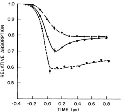
Many studies have characterized the behavior of excitons in GaAs quantum wells as the quantum confinement increases the thermal stability of the excitons to room temperature [23, 26, 27]. The excitonic absorption in a GaAs quantum well is shown in Figure 3.1 for
Figure 3.1Dynamics of the heavy hole exciton peak absorption as a function of time delay for non-resonant 300 K excitation (dashed line); resonant excitation at 300 K (solid line) and resonant 15 K excitation (dot-dashed line) showing the dramatic change in absorption.
Reprinted figure with permission from [27]. Copyright 1985 by the American Physical Society.
different excitation conditions: non-resonant excitations induces Coulomb screening, while resonant excitation produces bleaching of the excitonic absorption. The excitonic bleaching recovers to a value determined by Coulomb screening as the excitons are ionized by LO phonons in about 300 fs at 300 K. For 15 K, the LO phonon density is negligible and the resonant pumping produces a similar bleached absorption signature, followed by a recovery time on the order of 10 ps, indicating the fast recovery at room temperature is the result of phonon ionization of the excitons. The bleaching effect is attributed to phase-space filling of the single particle states during resonant excitation. Ionization by LO phonons produces carriers with about 25 meV of excess energy, creating higher temperature distributions and thereby reducing the band filling and screening effects. [27]