There is a rich collection of techniques proposed in the past for reducing peak switching activity during counterspeed testing of transient/delay faults. We propose algorithms for minimizing peak switching activity during counter-speed testing of stuck faults in sequential digital circuits under the combination-state-conserving scan (CSP scan) architecture (Potluri, 2015; Potluri et al., 2015).
NOTATIONS
Introduction
Power issues during at-speed testing
In the past, work has been done to reduce peak switching activity during combinational circuit testing (Dabholkar et al., 1998; Girard et al., 1998). For motivation, we will then discuss techniques proposed in the past to reduce peak switching activity during combinational circuit testing.
Reduction of peak power during testing of combi- national circuitsnational circuits
However, it should be noted that within the framework of the CSP-scan architecture (Potluri, 2015; Potluri et al., 2015), many algorithms for reducing peak switching activity during combinational circuit testing can be applied in a straightforward manner. to series circuits. Inductive effects on the power grid, which were negligible in earlier technologies, start to show and dominate the IR-drop on the power grid in sub-100 nm technologies (Pant, 2008; Pant et al., 2010).
Reduction of peak power during testing of sequen- tial circuitstial circuits
The interconnection scale places itself in a different way, on the feeder routing connections of the power grid. We solve the optimal test vector ordering problem for all the ITC circuits using an efficient BTSP heuristic.
Background
Related work in low power testing
Low power test vector generation is attractive as it reduces test power without modifying the design. In this thesis for both combinational and sequential circuits, it was shown how the vector rank test for the minimization of the peak capture power maps the Bottleneck Hamiltonian path problem, which is also NP-Hard.
Motivation for at-speed stuck-at testing
However, this additional phase of slow-speed block testing is, as the name suggests, slow, and therefore adds significantly to test times on modern systems-on-chips (SoCs), which are very complex. This motivates the need to minimize peak power dissipation during speed lock testing.
Design for Testability
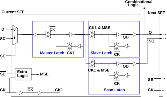
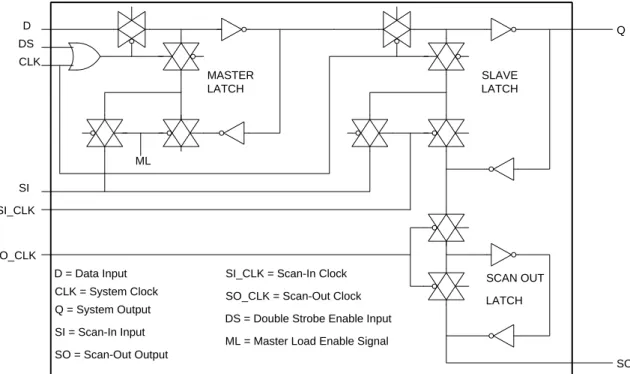
- Enhanced Scan (ES) scheme
- CSP-scan scheme
An improved scanning architecture was originally proposed in (Dervisoglu and Stong, 1991) for arbitrary two-vector applications for speed testing of sequential circuits. Since the majority of bits in these sequential circuits are unconcerned, filling the bits plays an important role in minimizing peak power during speed testing of sequential circuits.
An Efficient Test Vector Ordering Algorithm for Minimizing Peak Switching Activity
PITMP and BTSP
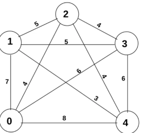
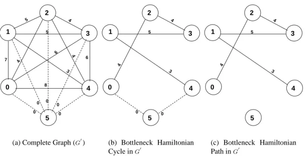
Next, to move the discussion forward, we will discuss the bottleneck traveling salesman path problem. Given an edge-weighted, undirected complete graphG, the Bottleneck Traveling Salesman Path Problem (BTSPP) is to find a Hamiltonian path inG such that the largest edge cost in this path is minimized.
Mapping of PITMP vs BTSP
- Mapping of PITMP to BTSP
- Mapping of BTSP to PITMP
Now, the ordering of vertices inP gives the optimal ordering of the test vectors such that the maximum Hamming distance between any two consecutive test vectors is minimized. Since the BTSP problem is NP-hard, it is easy to see that the PITMP problem is also NP-hard.
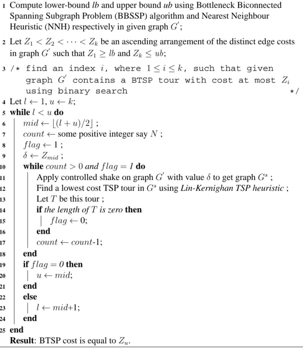
Algorithm for BTSP
Note that if G contains Hamilton tour with cost zero, then G′ contains a BTSP tour with at most cost δ. The while loop from lines 5 to 26 tries to find an index i where 1 ≤ i ≤ k such that given graphG′ contains a BTSP trip with at most priceZi using binary search. In line 21 of the algorithm, we are sure that the BTSP trip price inG′ is at most Zu.
In line24 in the algorithm, if we set lower bound to middle+, it does not mean that BTSP tour cost in G′ is at least Zl. Whenever this algorithm terminates, lower bound equal to upper bound and given graph contains a BTSP tour with cost at most Zu.
Experimental Results
- Experimental Setup
- Results
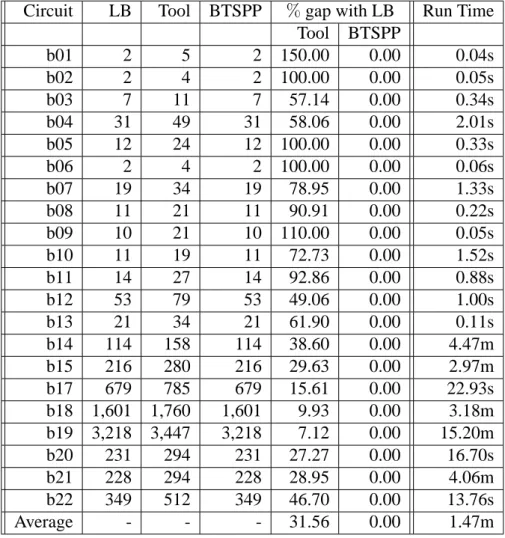
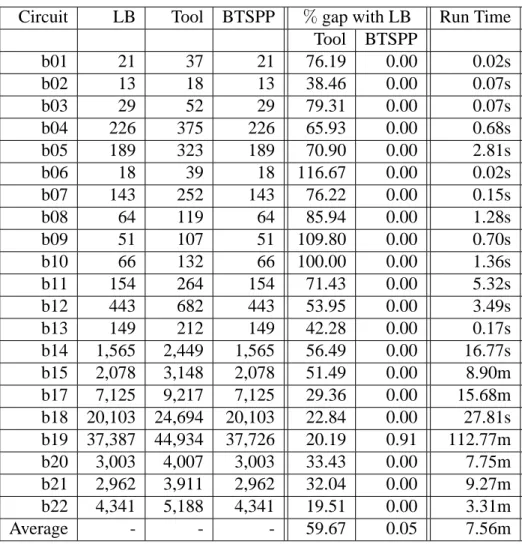
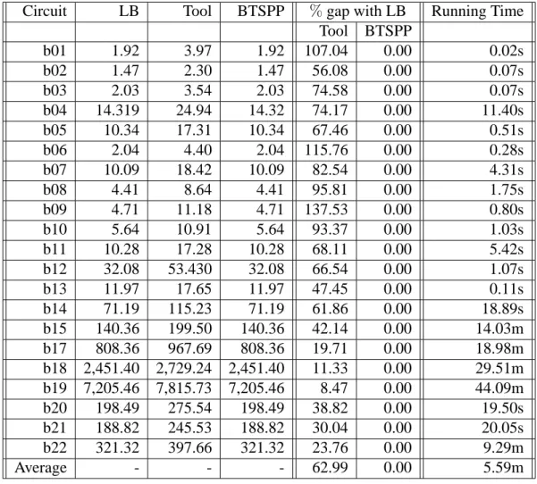
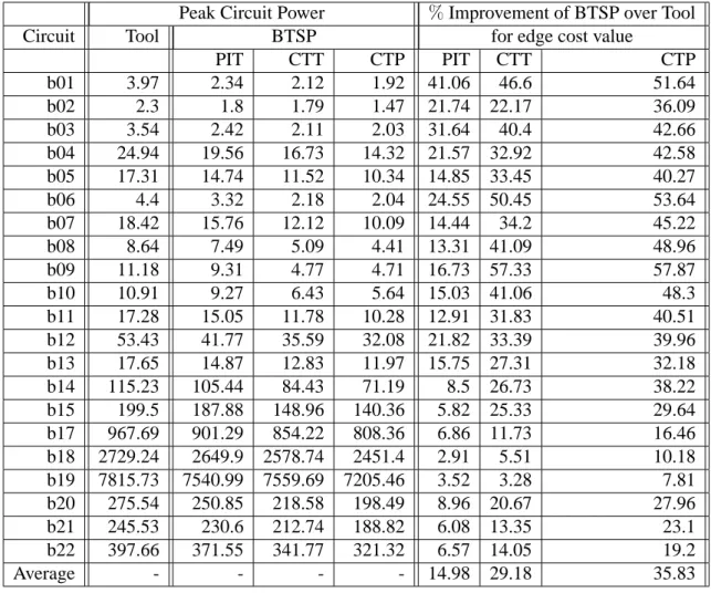
It compares the bottleneck value given by BT SP algorithm 3 and the maximum cost benefit value given by BBSS algorithm 2, and tries to tighten the lower bound value. In all three tables, LB corresponds to the lower bound obtained using the Enhanced Lower Bound Algorithm 4. Similarly, Tool and BTSPP correspond to the peak switches/power values in the obtained combinational circuit C, by applying the test vectors in the order suggested by the FastScanT M tool and the BTSPP algorithm respectively.
Similarly, Table 3.3 shows that when the total circuit shifts are used as the cost function, the maximum of the total shifts in C, obtained by applying the test vectors in the order suggested by the BTSPP algorithm is equal to the value of the lower bound low LB for all standards considered, except b19. On the other hand, the tip of the inC shift was obtained by applying the test vectors in the order suggested by.
Summary
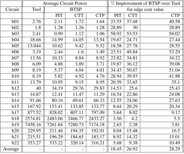
Since three different cost functions are considered, it is interesting to see the differences in using them. In addition, Table 3.6 shows that among the three cost functions, CTP is the best, followed by CTT and then PIT, in their effectiveness in saving power. Thus, one has to find a trade-off between power saving and computational efficiency by choosing the appropriate cost function among PIT, CTT and CTP cost functions for the test vector ordering process.
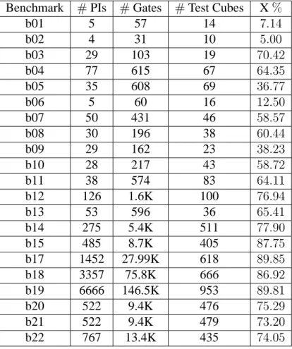
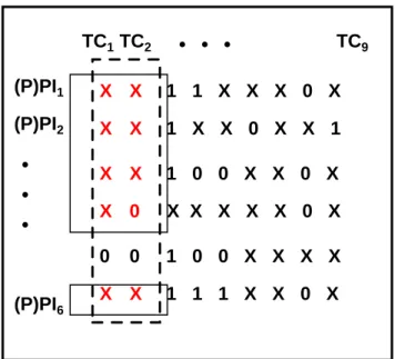
Typically, the test vectors generated by the ATPG tool tend to be dominated by bit (X) bits, especially for large circuits. However, it is possible to perform the X-bit padding and sorting of the test vectors in an integrated manner to achieve much better peak energy savings.
An Efficient X-filling algorithm for Minimizing Peak Switching Activity
- Peak Input Toggle Minimization Problem (PITMP)
- Balanced X-Filling (B-Fill) Algorithm
- Motivation
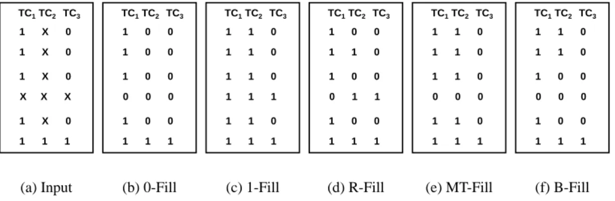
- Existing X-Filling Techniques
- Algorithm Details
- Test Cube Ordering Algorithm
- The Need for an Efficient Test Cube Order
- The X-Based Ordering Algorithm
- Effectiveness of X-Based Ordering Algorithm
- Integrated Test Vector Ordering and X-filling Algo- rithmrithm
- Experimental Results
- Experimental Setup
- Summary
The running time of this algorithm is O(mn), where is the number of bits in the test cube and is the number of test cubes. Before going into the details of the proposed integrated test cube ordering and X-filling algorithm, we will motivate the need for. Thus, the initial vectors have few X-bits, and the number of X-bits in each test cube decreases as we move further into the order given by the ATPG tool.
The running time of this algorithm ismax(O(nlogn), O(nm)), where is the number of bits in the test cube and is the number of test cubes. Output: TV = Order of fully specified input test vectors,bottleneck_value /* Rearrange the test cubes by interspersing the test cube.
An Optimal X-Filling algorithm for Minimizing Peak Switching Activity
Peak Input Toggle Minimization Problem (PITMP)
Bottleneck Coloring Problem (BCP)
- Problem Statement
- Dynamic Programming Algorithm to compute Lower-Bound (LB) for Bottleneck Coloring Problem(LB) for Bottleneck Coloring Problem
- Greedy Algorithm for Bottleneck Coloring Problem
- Proof of correctness
Suppose that at the end of an iteration imin stack contains an interval whose end time is less than or equal to i. Let j < i such that the number of intervals assigned to color injtitation is less than the lower bound. Letj < k < i such that in the kth iteration the above algorithm assigned color to an interval whose end time is more thani.
The number of intervals that have the color assigned to fromk+ 1thiteration equal to the bound below∗(i−k) and min stack contains an interval whose end time is equal and start time is greater thanks. This means the number of intervals whose start time is greater than thanks and end time is less than or equal toiis more than the lower bound ∗(i−k), which is a contradiction.
Optimal X-Filling Algorithm
- Motivation
- Algorithm Details
The end times and start times of all intervals assigned a color from 1st rep to rep are less than or equal to or greater than.
Test Vector Ordering Algorithm
- Motivation
- Algorithm Details
- Experimental Results
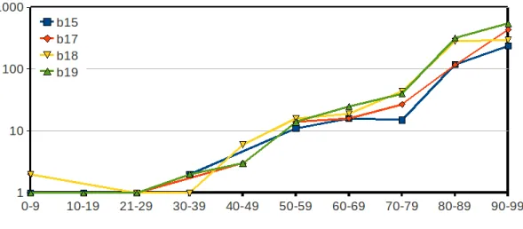
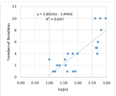
In Fig 5.2, the x-axis shows different don't-care sizes (0XX.X1 and 1XX.X0) and the y-axis shows the number of such don't-care regions for Tool, X-Stat and I-Ordering for b19. One can observe that I-Ordering increases the sizes of don't care regions exploited by the Algorithm 10.
Bottleneck Minimization Algorithm
Experimental Results
- Experimental Setup
- Results
The proposed technique outperforms all existing techniques and the percentage improvement consistently increases as the circuit size increases. The difference is due to the fact that the relationship between Peak Input Toggles and Circuit Toggles is not perfectly linear, and when we calculate the Peak Power of the Circuit, we must account for coupling capacitances. But our proposed method significantly outperforms all existing methods both in Peak Input Toggles and Peak Circuit Power.
In (Girard et al., 1998) it was shown that there is a strong correlation between input switches and internal switches within the circuit. Based on this assumption, we proceeded to find an optimal algorithm that minimizes the input switches to the circuit during the testing phase.
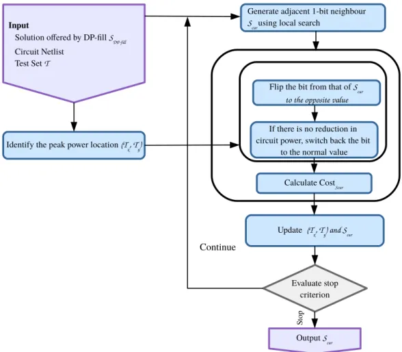
Local Search With Iterative 1-bit Neighbourhood
In the next section, we relax this assumption and try to search for solutions near the solution obtained so far using the local search technique and observe that the savings are marginal, thereby proving the effectiveness of the proposed technique. The color assigned by algorithm 10 called inline17 to this newly added interval captures the location of this shift in this subsequence. Peak Circuit Power (inµW) %Improvement of DP-Fill method over Circuit Tool ISA Adj-Fill XStat DP-Fill Tool ISA Adj-Fill XStat.
Circuit DP-fill DP-fill+ %Enhancement Addition DP-fill+ %Enhancement Addition (inµW) Unsaturated Shortening (inµW) Simulation Time SA Shortening (inµW) Simulation Time.
Summary
Conclusions
- Test vector ordering for fully specified test sets
- Simultaneous test vector ordering and don’t care fillingfilling
- An optimal algorithm for peak input switching ac- tivitytivity
- Future Work
However, the general problem of simultaneous sorting of the test vector and careless padding may not be best solved this way. Keeping this in mind, in this thesis, we focus on the simultaneous sorting problem of the test vector and do not care about padding. Thus, including careless padding as part of the optimization engine increases the robustness of the maximum power minimization engine.
Although this thesis suggests an optimal algorithm for don't care filling, for a given test cube order the global problem of minimizing input switching activity is also not optimally solved. The problem of optimal peak input switching activity by simultaneous test vector ordering and don't care filling is also an interesting open problem.
Li, ifill: An Impact-Oriented X-Filling Method to Reduce Move and Capture Power in Velocity Scan-Based Testing. Virazel, Efficient run-to-capture power reduction for the los scheme with x-filling based on adjacency probability. Chakrabarty, High-quality pattern selection for low-delay fault inspection considering process variation and crosstalk.
DFT-assisted techniques for peak launch-to-catch force reduction during launch-on-shift at speed testing. Saluja, Critical-path-aware X-filling for effective IR drop reduction in counter-speed scanning test.
List of publications based on the research work