The cores are based on the RISC-V ISA with support for some new custom instructions that help boost core performance. The core physical design result using commercial tools shows that it can reach a maximum frequency of 198.02 MHz with 0.036 mm2 area and 17.36 µW/MHz power requirement in 40 nm UMC technology node. The core consumes a dynamic power of 19.75 µW/MHz at 90 nm UMC, which is 36% and 40% better than the ARM Cortex-M3 and Cortex-M4, respectively, and also lower than many other cores.
The synthesis result at 65 nm shows that the kernel requires an additional 7% resources due to the integration of the proposed custom instructions. The core can perform an AES encryption in 63 clock cycles, while the same encryption requires 54265 and 19258 clock cycles in the proposed low-power and IoT cores, respectively.
LIST OF ACRONYMS
- Introduction
- RISC-V ISA
- RISC-V ISA
- Motivation
- Design Objectives
- Thesis Overview
Instruction set extensions can provide slightly different functionality depending on the width of the base integer instruction set. There are many examples in the literature to increase the processing capabilities of the processor. In the second phase of this work, we are concentrating on the data processing capabilities.
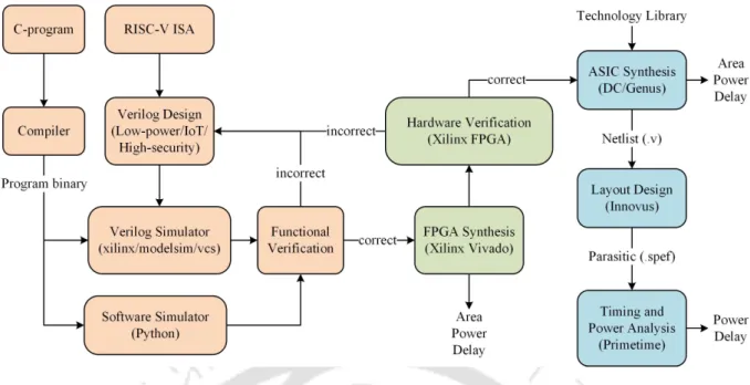
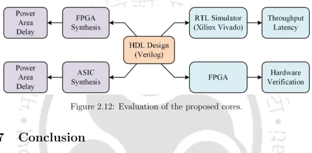
This chapter reports core area, power, and latency in FPGAs as well as ASICs. Core FPGA and ASIC results are reported in the core results section.
CHAPTER
LITERATURE AND METHODOLOGY
- Introduction
- Shakti
- PULPino
- Rocket SoC
- Existing Core Results
- Performance Measurement
- Power and Area Measurement
- Results
- Methodology
- Software Verification
- Hardware Verification
- Evaluation
- Conclusion
If the current instruction is independent of the instructions in the following stages, then it simply takes the operands from the Register file. In the case of branch instructions, the prediction of the Branch prediction unit is validated. Another common representation of the Dhrystone standard is DMIPS (Dhrystone MIPS) obtained when the Dhrystone result is divided by 1757 (the number of Dhrystones per second obtained on the VAX 11/780, nominally a 1 MIPS machine).
When the core (Verilog code) is ready for verification, the functionality of the core is first tested. If the output of the python environment and the Verilog simulator match, then the kernel functionality is correct.
![Figure 2.1: Shakti E class [1].](https://thumb-ap.123doks.com/thumbv2/azpdfnet/10342072.0/24.892.141.769.101.570/figure-shakti-e-class.webp)
DESIGN AND IMPLEMENTATION OF RISC-V CORE FOR LOW-POWER
APPLICATIONS
- Introduction
- Micro-architecture
- Instruction Fetch
- Instruction Decode
- Instruction Execute
- Register Write
- Results and discussion
- ASIC
- FPGA
- Conclusion
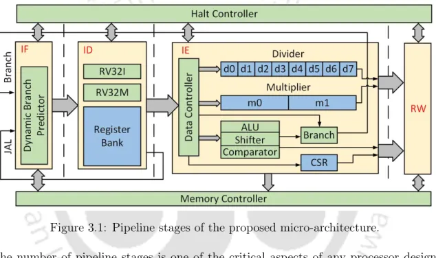
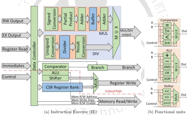
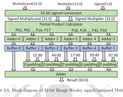
So, in the proposed microarchitecture, the basic core components like multiplier, divider, DBP, etc. are optimized for the best possible result. The critical path of the core is also optimized to achieve a peak frequency close to 200 MHz. The number of pipeline stages is one of the critical design aspects of any processor.
The pipelined stages of the proposed core are Instruction Fetch (IF), Instruction Decode (ID), Instruction Execute (IE), and Register Write (RW), as shown in Figure 3.1. Using this circuit directly in the IE stage increases the critical path of the overall system. The critical path of the first stage consists of 1 HA (Half Adder) and 29 FAs (Full Adders).
These three register write operations are performed through two write ports in the register bank. It can be seen that the core results are better than some of the existing micro-architectures, and it is suitable for low-power applications. The critical path delay of the proposed microarchitecture is 5.05 ns and 5.39 ns at UMC 40 nm and UMC 90 nm, respectively.
From Table 3.3, it can be seen that the energy efficiency of the proposed core is much higher than the other existing micro-architectures. The binary data is uploaded to the memory by the core of the FPGA to execute. For comparison, the FPGA result of the proposed microarchitecture is compared with some open source cores in Table 3.4.
DESIGN AND IMPLEMENTATION OF ADAPTIVE BINARY DIVIDER FOR
NUMBERS
- Introduction
- Literature Review
- Algorithm for Fixed-point Binary Divider
- Hardware Architecture of Fixed-point Binary Di- vider
- Single-precision Floating-point Divider
- FPGA Synthesis
- ASIC Synthesis
- Core Integration
- Conclusion
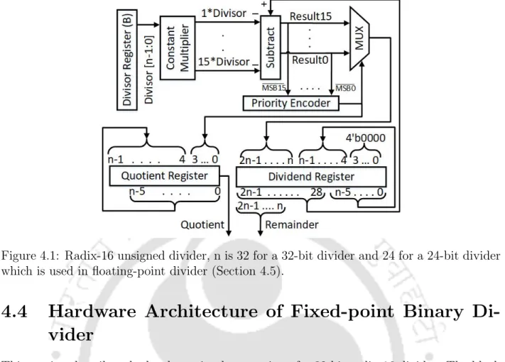
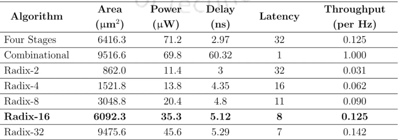
However, this number of iterations can be reduced depending on the location of the most significant (MSO) of the yield. In this way, the number of iterations can vary from 1 to 8 depending on the value of the yield. Because of this, the cost of the hardware implementation of the algorithm increases in terms of area, power and delay.
Thus, the use of shifters is preferred in the implementation of the constant multiplier circuit. The priority encoder output also gives the lower 4-bit of the quotient, as shown in Figure 4.1. Once the dividend mantissa is available, it is divided by the 24-bit mantissa of the divisor.
This step results in the maximum accuracy of the quotient in a minimum number of iterations. The design synthesis result shows that the proposed architecture can be implemented using 1271 LUTs and 140 slice registers. The ASIC synthesis of the proposed design is performed in a commercial synthesis tool, Synopsys DC (design compiler).
The maximum possible total delay of the proposed design is almost half compared to [56] and [58]. For comparison, the FPGA result of the proposed micro-architecture is compared with some open source cores in Table 4.4. From the analysis, it can be concluded that higher radix implementation of the proposed method is found more suitable for larger data widths.
DESIGN AND IMPLEMENTATION OF RISC-V CORE FOR DATA-CENTRIC IOT
- Introduction
- ISA and its Extension
- Micro-architecture
- Pipeline
- Results and Discussion
- ASIC
- FPGA
- Performance Measurement
- Conclusion
With the addition of these additional instructions, the computational performance and throughput of the proposed kernel are significantly increased. In this section, we will discuss the microarchitectural optimizations of the proposed kernel, which aim to increase the performance and efficiency of the kernel. First, the microarchitecture pipeline is described, followed by the individual core components.
Thus, an efficient multiplier circuit can improve the power, performance and surface efficiency of the core. The post-layout result of the proposed core is compared to some state-of-the-art cores in Table 5.2. The critical path delay of the proposed microarchitecture is 3.05 ns, which means that the core can operate up to a maximum frequency of 328 MHz.
The normalized value of dynamic power consumption of the proposed design is 26.44µW/MHz dynamic power. Once the functionality of the core is verified, various algorithms related to IoT applications such as AES, SHA-1, DCT, convolution etc. are run on the proposed core to measure its performance. To evaluate the performance of the proposed design, several benchmark applications are performed on the kernel.
To measure the performance of the proposed kernel, convolution is performed on two inputs, each with 10 samples. However, using the proposed extended instructions, the same convolution can be performed in 5343 clocks, which is about 37% better than the previous result. Core performance is measured by computing matrix multiplication, FIR filter, DCT, etc.
DESIGN AND IMPLEMENTATION OF RISC-V CORE FOR HIGH-SECURITY
APPLICATION
- Introduction
- ISA and its Extension
- Micro-architecture
- Instruction Fetch
- Instruction Decode
- Instruction Execute
- Results and Discussion
- ASIC
- FPGA
- Comparison of Proposed IoT and High-security ISA Extensions
- Conclusion
So the hardware multiply and divide circuits play a vital role in the overall area, power and performance of the core. Depending on the behavior of other circuit components, a radix-8 divider circuit is implemented to execute these instructions. A higher radix divider can provide better latency, but also increases circuit latency.
Therefore, the total design delay is ten clocks for a single 128-bit encryption. In the case of AES-L40, each circuit is divided into four sub-circuits, resulting in a circuit delay of 40 clocks. However, the scope and power of the design are improved by reusing the hardware resources of SubBytes, MixColumns, and AddRoundKey.
Similarly, AES-L160 has a data width of 8 bits and a delay Table 6.1: Synthesis results of AES hardware implementations on the UMC 65 nm technology node. The critical path delay of the proposed microarchitecture is 2.84 ns, which means that the core can operate up to a maximum frequency of 352 MHz. The critical path delay of the proposed microarchitecture is 2.81 ns, which means that the core can operate up to a maximum frequency of 356 MHz.
The compiled binary is loaded into the processor cache on the FPGA for execution. Design throughput is 0.27 Gbps during encryption and 0.26 Gbps during decryption. The throughput of the integrated AES core, core3, is 0.49 Gbps, which is very high compared to the other two cores.
CONCLUSION
Conclusion
In this work, we developed different core microarchitectures based on these two aspects. The micro-architectures are designed to get maximum performance with a minimum requirement of area and power. Two ISA extensions, EX1 and EX2, are also proposed for data-centric IoT and high-security applications.
In this work, we proposed three 32-bit core microarchitectures targeting applications: low-power, data-centric IoT devices, and high security.
Summary of Contributions
Future Directions
PUBLICATIONS
BIBLIOGRAPHY
Kamakoti, “SHAKTI-F: A Fault Tolerant Microprocessor Architecture,” in 2015 IEEE 24th Asian Test Symposium (ATS), pp. Asanovic, “The RISC-V Instruction Set,” in Poster op het Symposium on High Performance Chips ( HotChips-25), Stanford, CA, augustus 2013. Kamakoti, "SHAKTI Processors: An Open-Source Hardware Initiative," in 2016 29th International Conference on VLSI Design en 2016 15th International Conference on Embedded Systems (VLSID), pp.
Vivian, "Out of order floating point coprocessor for RISC V ISA", in 2015 19th International Symposium on VLSI Design and Test, pp. Samyal, "Dynamic branch prediction modeller for risc architecture", in 2013 International Conference on Machine Intelligence and Research Advancement , pp. Agosta, “Tailored Instruction Set Extensions for a Tightly Coupled Ultra-Low Power Cluster of Open Cores,” in 2015 IFIP/IEEE International Conference on Very Large Scale Integration (VLSI-SoC), pp.
Patel, "Design of high performance digital divider," i 2020 IEEE VLSI DEVICE CIRCUIT AND SYSTEM (VLSI DCS), s. Takagi, "A hardware algorithm for integer division," i 17. IEEE Symposium on Computer Arithmetic (ARITH'05), s. Muller, "Variable radix real and complex digit-recurrence division," i 2005 IEEE International Conference on Application-Specific Systems, Architecture Processors (ASAP'05), pp.
Motomura, "Low latency divider using ensemble of moving average curves," i 2017 18th International Symposium on Quality Electronic Design (ISQED), s. Sasamal, "Design and synthesis of goldschmidt algorithm based floating point divider on fpga," i 2016 International Conference om kommunikation og signalbehandling (ICCSP), s. Lammel, "The future of mems sensors in our connected world," i 2015 28th IEEE International Conference on Micro Electro Mechanical Systems (MEMS), pp.
![Figure 2.2: Shakti C class [1].](https://thumb-ap.123doks.com/thumbv2/azpdfnet/10342072.0/25.892.141.781.133.650/figure-shakti-c-class.webp)
![Figure 2.3: Block diagram of RI5CY core [2].](https://thumb-ap.123doks.com/thumbv2/azpdfnet/10342072.0/27.892.137.771.100.516/figure-block-diagram-of-ri-cy-core.webp)
![Figure 3.6: Comparison of Dhrystone and CoreMark scores with other commercial cores [4,5].](https://thumb-ap.123doks.com/thumbv2/azpdfnet/10342072.0/47.892.115.808.158.557/figure-comparison-dhrystone-coremark-scores-commercial-cores.webp)
