In partial fulfillment of the requirement for the award of the Doctor of Philosophy degree. The work contained in this thesis entitled "Growth and study of the optoelectronic properties of a-Si:H/nc-Si:H Based Superglass Structures" was carried out by me under the direction of Dr. This thesis does not contain any previous material. presented for the award of any degree or diploma.
This confirms that the work in this thesis entitled "Growth and study of optoelectronic properties of superlattice structures based on a-Si:H/nc-Si:H". This work has not been submitted anywhere else for the award of any degree or diploma.
Acknowledgements
A lower band gap superlattice structure such as a-Si:H/nc-Si:H is desirable to increase carrier mobility. The a-Si:H/nc-Si:H superlattice structures show many interesting properties such as low thermal conductivity, enhanced carrier mobility and photoconductivity, visible photoluminescence, etc. The present thesis focuses on the study of the interface states in a-Si:H/nc-Si:H superlattice structures , which play an important role in tuning the optoelectronic properties of these structures.
The a-Si:H/nc-Si:H superstructures were prepared using HWCVD and rf-PECVD techniques. For the individual thin layers of a-Si:H and nc-Si:H thin films, the rf-PECVD technique was used, while for the thick films, the HWCVD technique was used. Si:H superlattice structures, therefore, optimization of the deposition parameters for device quality fabrication of a-Si:H, nc-Si:H using HWCVD and rf-PECVD techniques was first performed and then from the optimized parameters of the deposition Supergrit a-Si:H/nc-Si:H structures were fabricated.
Quite interestingly, room temperature persistent photoconductivity (PPC) has been observed in these a-Si:H/nc-Si:H superlattice structures in coplanar geometry. Whereas, transverse geometry has been used to estimate the density of localized states in single layers as well as superlattice structures of a-Si:H and nc-Si:H thin films using space charge current limited (SCLC) measurements.
LIST OF ABBREVIATIONS AND SYMBOLS
CONTENTS
Structural and optoelectronic properties of a-Si:H and nc-Si:H
Laser Induced Selective Crystallization of Amorphous Silicon
Persistent Photoconductivity studies in a-Si:H/nc-Si:H
Density of states measurement in a-Si:H/nc-Si:H superlattice
Tunable visible photoluminescence in a-Si:H/nc-Si:H superlattices 133
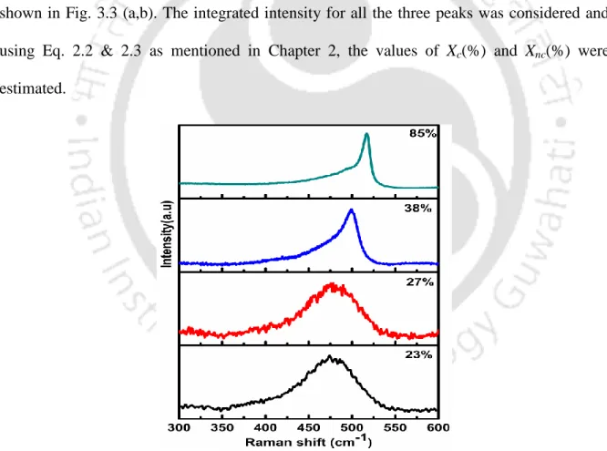
4.1 (a) Raman spectra at different laser power density ([R] = 50%), (b) Deconvolved Raman spectra of the film after laser power irradiation. 4.2 (a) Raman spectra at different laser power density for the film prepared at ([R]=62%), (b) Deconvolved Raman spectra of the film after. 4.3 (a) Raman spectra at different laser power densities for the film fabricated at [R] = 94%, (b) Deconvolved Raman spectra of the film after irradiation.
4.6 (a) Raman spectra at different laser power density (rf power = 40 W), (b) Deconvolved Raman spectra of the film after laser irradiation. 4.7 (a) Raman spectra at different laser power density (rf power = 60 W), (b) Deconvolved Raman spectra of the film after laser irradiation. 7.3 (a) Raman spectra of single-layer a-Si:H and nc-Si:H thin films with different [R], (b) Deconvolved Raman spectra of single-layer nc-Si:H.
LIST OF TABLES
Contents of Thesis Chapters
Chapter 2, which gives a description of the details of the sample preparation techniques such as HWCVD and rf-PECVD, as well as the details of the deposition parameters that were used to prepare a-Si:H, nc-Si:H and a. - Si:H/nc-Si:H supergrinding structures. This chapter also provides a brief discussion on the various characterization techniques used to analyze the structural, optical, and electrical properties of Si thin films. The decay time constant of PPC, its dependence on exposure time, electric field, number of cycles and annealing temperature are discussed in detail.
The dissertation work concludes with scope for future work from the current research.
Roca i Cabarrocas, Plasma enhanced chemical vapor deposition of amorphous, polymorphic and microcrystalline silicon films, Journal of Non-Crystalline Solids. Taylor, ESR study of the hydrogenated nanocrystalline silicon thin films, Journal of Non-Crystalline Solids. Shah, Microstructure and open circuit voltage of n-i-p microcrystalline silicon solar cells, Journal of Applied Physics.
Wang, Optical and electronic properties of microcrystalline silicon as a function of microcrystallinity, Journal of Applied Physics. Vaněček, Spectral response of amorphous-nano-crystalline silicon thin films, Journal of Non-Crystalline Solids. Gallagher, Production of high-quality amorphous silicon films by surface decomposition of volatile silane, Journal of Applied Physics.
Matsumura, Study on catalytic chemical vapor deposition method to prepare hydrogenated amorphous silicon, Journal of Applied Physics. Schubert, Amorphous and microcrystalline silicon by hot wire chemical vapor deposition, Journal of Applied Physics.
Preparation of Si thin films
- Description of Hot Wire Chemical Vapor Deposition (HWCVD) technique In this method, the precursor gases are decomposed thermally and catalytically into different
- Description of rf-Plasma Enhanced Chemical Vapor Deposition (rf-PECVD) technique
- Preparation of a-Si:H and nc-Si:H thin films using both HWCVD and rf- PECVD techniques
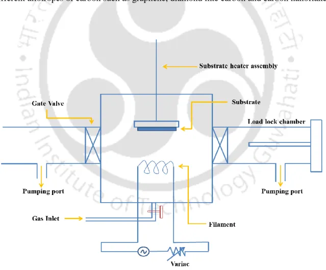
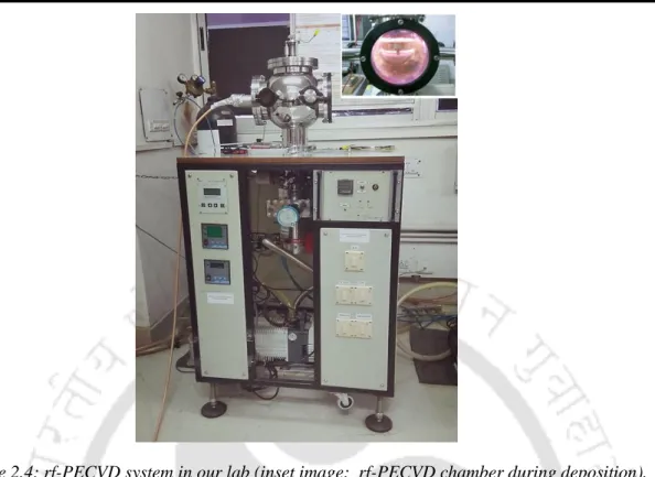
The schematic diagram of a HWCVD system is shown in Fig. 2.1, while fig. 2.2(a) and (b) show the photograph of the entire HWCVD system and the HWCVD chamber during deposition, respectively. A dual wavelength pyrometer from IRCON (model MR-OR05-240) was used to measure filament temperature during deposition. The filament as well as the gas inlets are surrounded by SS gas containment cup which facilitates the effective dissociation of the gases.
This system has also been used to fabricate other semiconductor materials, such as SiC thin films, various allotropes of carbon, such as graphene, diamond-like carbon, and carbon nanoflakes. Unlike the PECVD technique, where SiH3 is the main film-forming radical, in HWCVD, Si and H are the primary radicals released from the filament surface [25, 26]. Capacitively coupled PECVD method with radio frequency 13.56 MHz is widely chosen by the scientific community to produce device grade films and is also used in industrial applications [28–31].
The system consists of a high vacuum chamber connected to a gas inlet and the source of the discharge. Highly pure (>99.99%) semiconductor grade silane (SiH4) and hydrogen (H2) were used as precursor gases to fabricate silicon thin films. The first event for the growth of micro, nano and amorphous silicon is the breakdown of the source gas by glow discharge plasma.
These gases are dissociated into various film-forming radicals by an inelastic collision with the high-energy electrons (about several ten electron volts) present in the plasma, followed by subsequent gas-phase reactions. Of these radicals, SiH3 is the least reactive and has the highest concentration, regardless of the initial formation rate, and is thus mainly responsible for the growth of micro- and nanocrystalline and a-Si thin films. Furthermore, excitation of the ground state electron to the vacuum state gives rise to ionization events.
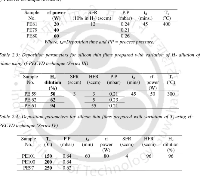
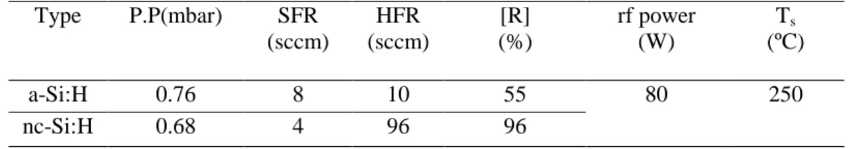
As discussed in the previous chapter, the motivation behind this thesis has been to obtain unit quality a-Si:H and nc-Si:H films and subsequent preparation of a-Si:H/nc-Si:H. To achieve this, four different series of samples were prepared (using HWCVD and rf-PECVD techniques) by varying one deposition parameter at a time while keeping all the other parameters fixed; Series I: the variation of H2 dilution (23-85%) of SiH4 on thin silicon films produced by HWCVD technique, Series II: the variation of rf power (20-60 W) on thin silicon films produced by rf- PECVD technique, Series III: the variation of H2 dilution (50-94%) of SiH4 on thin silicon films produced by rf-PECVD technique, Series IV: the variation of substrate temperature (150 ºC-250 ºC) on thin silicon film produced by rf -PECVD technique. For the TEM studies, thin films with thickness < 40 nm were also deposited on carbon-coated Cu grid (Mesh 400).
P (mbar)
- Preparation of a-Si:H/nc-Si:H superlattice structures using both HWCVD and rf-PECVD techniques
- Characterizations techniques .1 X-ray diffraction (XRD)
- Raman Spectroscopy
- Transmission electron microscopy
- Field emission scanning electron microscopy
- Stylus profilometer
- UV-Vis NIR transmission Spectroscopy
- Photoluminescence
- Electrical transport measurements
- References
- Measurement Details
- The effect of variation of H 2 dilution of SiH 4 on silicon thin films prepared using HWCVD technique (Series I)
- Structural properties .1 X-ray Diffraction
- Optical properties
- Electrical properties
- The effect of variation of rf-power on silicon thin films prepared using rf-PECVD technique (Series II)
- Structural properties .1 X-ray Diffraction
- Optical properties
- Electrical properties
- The effect of variation of hydrogen dilution of SiH 4 on silicon thin films prepared using rf-PECVD technique (Series III)
- Structural Properties .1 X-ray Diffraction
- Optical properties
- Electrical properties
- The effect of variation of substrate temperature on silicon thin films prepared using rf-PECVD technique (Series IV)
- Structural Properties .1 X-ray Diffraction
- Optical properties
- Electrical properties
- Conclusion
- References
- Measurement Details
- Results and Discussion
- Conclusion
- References
- Measurement Details
- Results and Discussion
- Conclusion
- References
- Measurement Details
- Theory
- Results and Discussion
- Conclusion
- References
- Measurement Details
- Results and Discussion
- Conclusion
- References
- Scope for Future work
- Asha Yadav and Pratima Agarwal, “Laser Induced Selective Crystallization of Amorphous Silicon Thin Film for Device Applications”, Materialstoday
- Asha Yadav and Pratima Agarwal, “Optoelectronic properties of silicon thin films for solar cell application: Influence of hydrogen dilution”, Frontier Energy Research with
- Asha Yadav, Venkanna Kanneboina and Pratima Agarwal, “Comparative studies of microstructure of silicon thin films by Raman spectroscopy and electrical transport
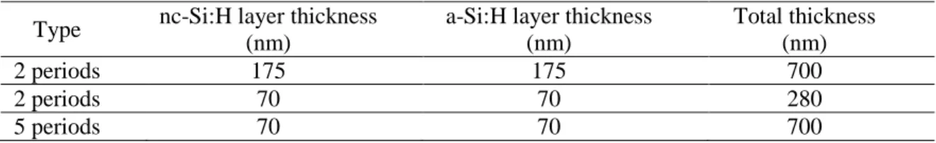
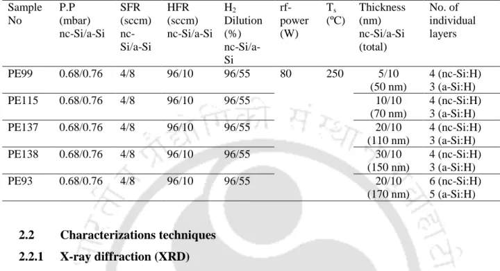
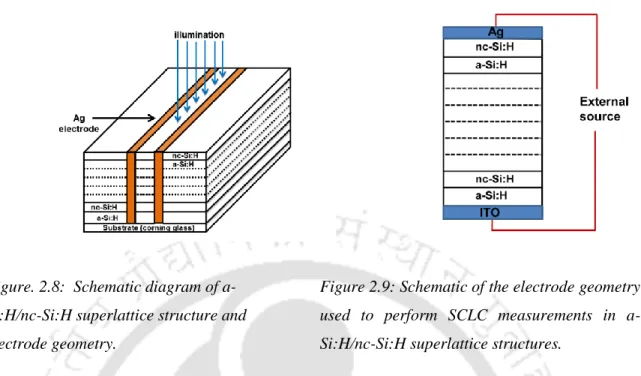
The individual layer thicknesses of a-Si:H and nc-Si:H in the superlattice structures are listed in Table 2.5. In these superlattice structures, the bottom and top layers were retained as nc-Si:H. The a-Si:H and nc-Si:H sublayers were prepared by varying the hydrogen dilution [R] in silane.
The electrical transport properties across the superlattice structures of a-Si:H and nc-Si:H thin films were measured in both coplanar and transverse geometry. Structural and optoelectronic properties of a-Si:H and nc-Si:H thin films prepared by HWCVD and rf-PECVD. For the PPC studies, single and multilayer/superlattice structures of a-Si:H and nc-Si:H thin films prepared using both rf-PECVD and HWCVD techniques were used.
For the preparation of thick (≥50 nm) individual layers of a-Si:H and nc-Si:H films in these superlattice structures, HWCVD technique was used. Superlattice structures consisting of two (02) and five (05) periods of alternate layers of a-Si:H and nc-Si:H were prepared using HWCVD technique on corning 1737 glass substrate. In this chapter, density of states (DOS) studies on single layers and superlattice structures of a-Si:H and nc-Si:H thin films were presented.
6.5(a)) may arise due to the presence of interfacial states between a-Si:H and nc-Si:H layers in these superlattice structures. In this process, some of the electrons are trapped in the bulk density of states of a-Si:H as well as the interfacial states between a-Si:H and nc-Si:H. Superlattice structures with thin individual layers of nc-Si:H and a-Si:H were fabricated using rf-PECVD.
a-Si:H and nc-Si:H thin films were prepared by varying the hydrogen dilution [R] of the silane while keeping all other deposition parameters fixed. No photoluminescence was observed for thin and thick monolayer films of a-Si:H and nc-Si:H. The origin of PPC in these superstructures is understood to be the trapping of charge carriers at the interfaces between the a-Si:H and nc-Si:H film substrates.
We fabricated nc-Si:H/a-Si:H superlattice structures with different thicknesses (d) of the nanocrystalline Si layers. From the optimized deposition parameter using both the techniques, a-Si:H/nc-Si:H superlattice structures were fabricated. The motivation of the present thesis work was to study the role of the interface conditions in a-Si:H/nc-Si:H superlattice structures on the optoelectronic properties of these structures.
In these a-Si:H/nc-Si:H superlattice structures, persistent room-temperature photoconductivity (PPC) was observed in the coplanar geometry.
![Figure 1.1: Continuous random network (CRN) allowing the constituent atoms to retain their coordination numbers [76]](https://thumb-ap.123doks.com/thumbv2/azpdfnet/10541938.0/37.918.162.787.499.921/figure-continuous-random-network-allowing-constituent-coordination-numbers.webp)
![Figure 1.3: Schematic of the dissociation processes of SiH 4 and H 2 molecules under the influence of high rf-field [97]](https://thumb-ap.123doks.com/thumbv2/azpdfnet/10541938.0/42.918.239.650.117.391/figure-schematic-dissociation-processes-sih-molecules-influence-field.webp)

![Figure 3.6: UV-Vis-NIR transmission spectra for the Si thin films prepared at different [R]](https://thumb-ap.123doks.com/thumbv2/azpdfnet/10541938.0/93.918.155.758.563.991/figure-vis-nir-transmission-spectra-films-prepared-different.webp)
