Certified that the work described in this thesis entitled "Hierarchical Metal Oxides for Photoelectrochemical Water Oxidation and Sensing Applications" by Mr. Electrochemical Impedance Spectroscopy (EIS) Analysis Charge Injection and Separation Efficiency (Hole Scavenger) Electrochemical Surface Area (ECSA) Analysis.
Thesis Overview
- Recent advances in the design and development of semiconductor metal oxides, based on their morphologies and hetero-structures, enhances the charge transport as well as the light-harvesting
- Co(OH)F as a Noble Metal-Free Redox Mediator and Hole Extractor for Boosted Photoelectrochemical Water Oxidation in Worm-like Bismuth Vanadate
- Bio-template Assisted Hierarchical ZnO Superstructures Coupled with Graphene Quantum Dots for Enhanced Water Oxidation Kinetics
- Ultrasensitive NO X detection in Simulated Exhaled Air: Enhanced Sensing via Alumina Modification of In-situ Grown WO 3 Nano blocks
GQDs provide additional driving force for hole extraction from the BiVO4 surface, due to the presence of negatively charged species and transfers in CoSn-LDH, which accelerate hole transport in the electrolyte for enhanced water oxidation reaction. Therefore, Co(OH)F nanorods were designed as an efficient catalyst and coupled with BiVO4 photoanode for efficient photoelectrochemical oxidation of water.
Introduction and literature survey
Global Energy Outlook
In recent years, global energy consumption has increased significantly and is expected to increase continuously in the near future. If the emission rate of fossil fuels continues in this way, the greenhouse gases that accumulate in the atmosphere will pose a serious threat to the environment.
Renewable Energy Sources
According to the report of the Intergovernmental Panel on Climate Change (IPCC), the temperature increase due to global warming should not exceed 2˚C and the carbon dioxide content in the atmosphere 450 ppm, to avoid the catastrophic consequences3-4. Among the various techniques used to produce H2 fuels, photoelectrochemical water splitting is fascinating and has the potential to become an extensive pathway for future energy production.

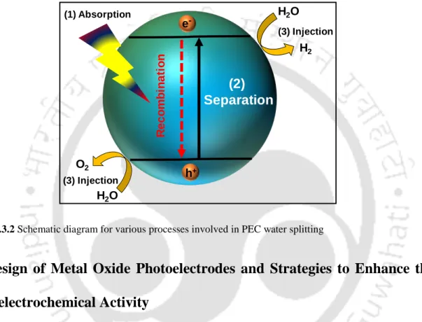
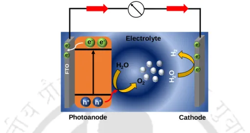
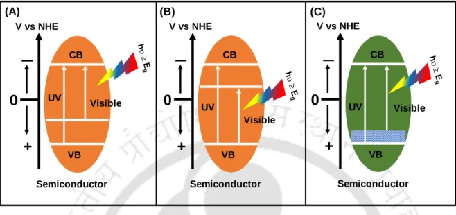
Photoelectrochemical (PEC) Water Splitting
Therefore, a semiconductor must have a suitable band gap as well as band positions for effective water splitting reactions. Due to the multi-electron transfer involved in the reaction mechanism of water oxidation, it generally requires high overpotentials due to the sluggish kinetics of the photoanode.
Design of Metal Oxide Photoelectrodes and Strategies to Enhance the Photoelectrochemical Activity
- Electronic Structure Modification by Foreign Element Doping
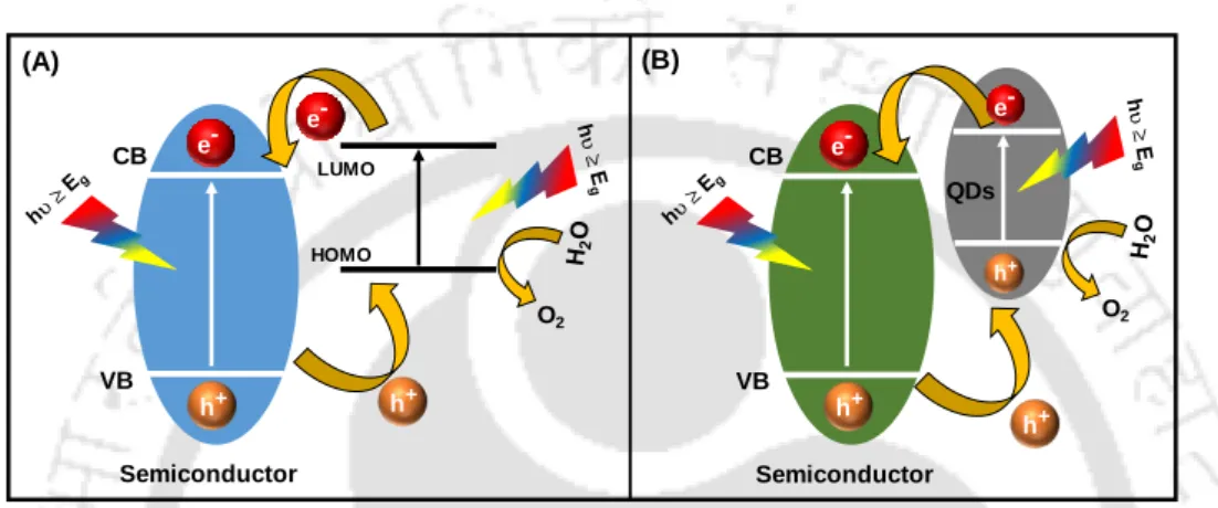
- Dye and Quantum Dot Sensitization
- Construction of Different Heterojunctions
- Co-catalysts Modification
- Hybridization with Hole/Electron Extracting Layer
Furthermore, self-doping and co-doping are equally important strategies to improve PEC performance. Therefore, incorporating electron/hole extracting materials to extract photogenerated electrons and holes is another possible approach to improve the PEC performance.
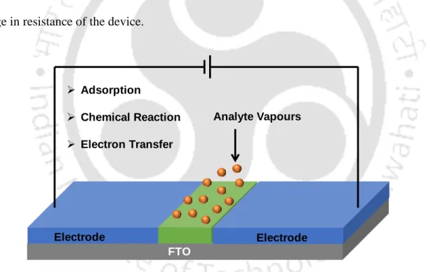
Metal Oxide Based Chemiresistor Sensors
- Working Principle of Chemiresistor Sensor Device
Surface-induced adsorption, desorption, and oxidation reactions of the exposed analyte with the sensor material are primarily responsible for this change in resistance. Achieving high selectivity is probably one of the major challenges when designing a metal oxide-based sensor.
Motivation and Objectives of the Present Work
The main drawback related to this type of technique is its inclusion in portable real-time devices, due to the large size of the devices, operational difficulties and high cost146-147. Although several strategies have been applied to improve the surface properties of the photoanode, the main properties of the photoanode are also the limiting factors for the recombination losses of charge carriers before they come to the surface for chemical reactions.
A brief discussion of the performance parameters of photoelectrochemical water splitting coupled to the photoanodic materials is also included. Finally, this chapter includes the fabrication of a two-terminal Chemiresistor sensor device, along with a brief discussion of performance parameters.
Introduction
Chemicals and Materials Used
Characterizations of as-synthesized Materials, Photoelectrochemical and Chemiresistor Devices
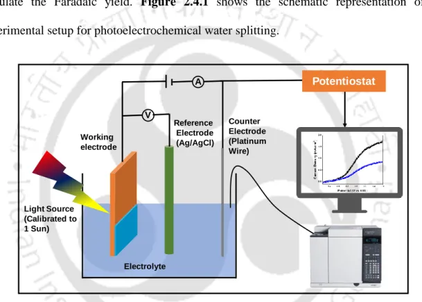
Photoelectrochemical Measurements
Electrochemical impedance spectroscopy (EIS) measurements were performed using the CH Instruments model CHI680E, Inc., Austin, TX, in the frequency range from 0.1 Hz to 106 Hz under light illumination. Mott-Schottky plots for all photoanodes were measured over a DC potential range of -1 to +1 V vs Ag/AgCl under dark conditions with an applied frequency of 1 kHz.
Photoelectrochemical Performance Parameters
- Quantum Efficiency Measurement of a Photoelectrochemical Device
- Faradaic Yield
- Applied Bias Photon-to-Current Efficiency (ABPE)
Where Jabs is the photocurrent density after the complete conversion of absorbed photons into current, ηinj represents the hole injection efficiency and ηsep represents the charge separation efficiency, respectively, can be expressed by equation 2.4 and 2.5. Faradaic yield calculation is the most useful technique to understand that the obtained photocurrent is solely due to water oxidation and not the photocorrosion of photoanode or other side reactions.
Electrochemical Impedance Spectroscopy (EIS) Analysis
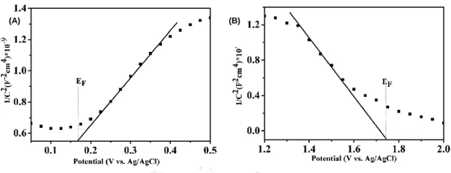
Another important parameter that affects the performance of a photoelectrode is the charge carrier density, determined by the Mott-Schottky (M-S) analysis. Where C is the capacitance of the semiconductor, e is the charge of an electron, E is the applied potential, A is the surface area of the photoelectrode, ɛ is the dielectric constant of the semiconductor, ɛ0 is the permittivity of free space, ND is the charge carrier density of semiconductor, k is the Boltzmann constant and T is the temperature.
Fabrication of a Two-Terminal Chemiresistor Sensor Device
- Gas Sensing Assembly
- Gas Sensing Performance Parameters
- References
- Introduction
- Experimental Section
- Fabrication of BiVO 4 Photoanode (Scheme , Step 1-2)
- Hydrothermal Synthesis of Graphene Quantum Dots (GQDs)
- Fabrication of BiVO 4 /GQDs Photoanode (Scheme 3.2.1, Step 3)
- Results and Discussions
- Powder X-ray Diffraction (XRD) Analysis
As obtained BiVO4/GQDs/CoSn-LDH photoanodes were rinsed with distilled water and dried at 60˚C. Trace (d) represents the XRD pattern for BiVO4/GQDs/CoSn-LDH photoanode, showing the preservation of the crystal structure of BiVO4 after the immobilization of GQDs and CoSn-LDH.
2 Degree
GQDs/CoSn-LDH
- Fourier Transform Infrared Spectroscopy (FT-IR) Analysis
- Raman Spectroscopy Analysis
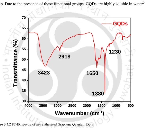
The two peaks at 1650 cm-1 and 1380 cm-1 belong to the asymmetric and symmetric vibrations of the –COOH group. The D band is due to the bonding and antibonding orbitals of the sp3 atoms with the A1g phonon breathing mode caused by defects, while the G band is due to the in-plane stretching vibrations of the sp2 ordered carbon atoms with E2g optical phonons.
Wavenumber (cm -1 )
To identify the functional groups attached to GQD, FT-IR analysis was performed, and Figure 3.3.2 presents the same. The Raman spectra of the synthesized GQDs as shown in Figure 3.3.3 show two distinct peaks at 1377 cm-1 and 1547 cm-1, corresponding to the D and G band respectively.
GQDs
UV-Visible and Photoluminescence Spectra Analysis
UV-Vis spectra of GQDs consist of two distinct peaks at 250 nm and 340 nm corresponding to. A strong and sharp emission peak at 430 nm was observed with excitation at 340 nm indicative of the fluorescent nature of GQDs.
Raman Shift cm -1
In order to investigate the optical properties of the synthesized GQDs, UV-Visible and Photoluminescence spectra were recorded, and Figure 3.3.4 presents the same.
GQDs G
Morphological and Structural Analysis
Detailed observations for the morphological evolution of as-synthesized BiVO4, BiVO4/GQDs, BiVO4/CoSn-LDH and BiVO4/GQDs/CoSn-LDH were characterized using FESEM analysis, as depicted in Figure 3.3.5. From trace (G), it is clear that a thin layer of CoSn-LDH is packed over the BiVO4 surface.
GQDs
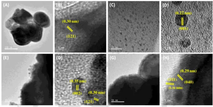
Furthermore, the typical size of the synthesized GQDs is found to be 4.7 nm. The HRTEM image of GQD-coated BiVO4 reveals well-defined lattice fringes with an interplanar spacing of 0.30 nm correspond to the (121) plane of BiVO4 while a d-spacing of 0.35 nm corresponds to (002) graphite plane.
CoSn
- X-ray Photoelectron Spectroscopy (XPS) Analysis
- Time-resolved Photoluminescence (TRPL) Analysis
- Photoelectrochemical Measurements
- Electrochemical Impedance Spectroscopy (EIS) Analysis
- Charge Injection and Separation Efficiency (Hole Scavenger)
- Electrochemical Surface Area (ECSA) Analysis
- Mott-Schottky Analysis
- Cyclic Voltammetry Analysis
- Zeta Potential Analysis
- Mechanism for Enhanced Water Oxidation Kinetics
- Conclusions
- References
After the decoration of BiVO4 with GQDs and CoSn-LDH, the BiVO4/GQDs/CoSn-LDH photoanode shows two peaks for Bi(4f), i.e. From Figure 3.3.13 (B), it is clear that BiVO4/GQDs/CoSn- LDH photoanode shows an impressive IPCE value of.
Introduction
Due to the multi-electron transfer involved in the reaction mechanism of water oxidation, it generally requires high overpotentials due to the sluggish kinetics of the photoanode. The conductivity, as well as the charge mobility, is improved due to the presence of Fluoride in Co(OH)F, thereby improving the electrocatalytic activity30-31.
Experimental Section
- Synthesis of BiVO 4 over FTO
- Hydrothermal Synthesis of Co(OH)F
- Fabrication of BiVO 4 /Co(OH)F Photoanode
Briefly, for the preparation of BiVO 4 /Co(OH)F composite, a calculated amount of Co(OH)F (5 mg/ml) was dissolved in ethanol via sonication for 30 minutes. These drop cast films were dried in an electric oven at 60°C for 12 hours.
Results and Discussions
- Powder X-ray Diffraction (XRD) Analysis
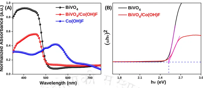
- UV−Visible Absorption Spectra Analysis
- Morphological and Structural Analysis
- X-ray Photoelectron Spectroscopy (XPS) Analysis
- Photoelectrochemical Measurements
Figure 4.3.1 X-ray diffraction pattern of (A) electrodeposited BiVO4, indexed to monoclinic phase (black line), (B) as-synthesized Co(OH)F nanorods, indexed to orthorhombic phase (red line) and (C) ) BiVO4/Co (OH)F composite (burgundy line) shows signature peaks for both compounds ( Indicates FTO). Figure 4.3.3 Typical FESEM images (top view) of (A) as-deposited BiOI film showing nano-flake structures (B) representing FESEM images of BiVO4 showing worm-like structures (C) as-synthesized Co(OH)F showing nanorods and (D) FESEM image of BiVO4/Co(OH)F composite.
Co(OH)F_Fitted BiVO 4 /Co(OH)F
Co(OH)F_Fitted
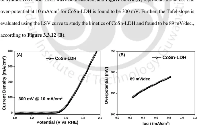
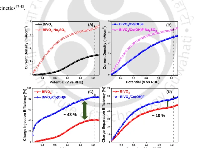
To compare the water oxidation kinetics as a function of the redox couple, a systematic study of water oxidation involving Co(OH)F and BiVO4 has been carried out. The PEC performance was analyzed using Linear Sweep Voltammetry (LSV) as a function of applied bias, shown in Figure 4.3.9.
Time (ns)
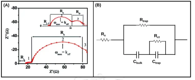
Electrochemical Impedance Spectroscopy (EIS) Analysis
The arc radius in the Nyquist curve was due to charge transfer at the electrolyte/electrode interface. In the case of BiVO4/Co(OH)F, the charge transfer resistance was 2.36 K suggesting enhanced interfacial transport of charges with minimal contact resistance.
Co(OH)F Fitted
- Charge Injection and Separation Efficiency (Hole Scavenger Test)
- Electrochemical Surface Area (ECSA) Analysis
- Faradaic Yield and Stability Measurements
- Conclusions
- References
As observed from figure 4.3.14 (C) that the hole injection efficiency of BiVO4/Co(OH)F photoanode increased dramatically compared to pristine BiVO4. The photoelectrochemical operational stability was performed at 1.23 V vs. RHE under continuous illumination for 5 h shown in Figure 4.3.16 (B).
Bio-template assisted hierarchical ZnO superstructures coupled with graphene quantum dots for water oxidation
Introduction
For this, 2D materials such as reduced graphene oxide (RGO) have been widely used to assist the photogenerated electron–hole separation23. In particular, due to their size-dependent electronic and optical properties, quantum dots have attracted considerable attention.
Experimental Section
- In-situ Growth of Hierarchical ZnO Superstructures onto Fluorine Doped Tin Oxide Substrate
- Synthesis of Graphene Quantum Dots (GQDs)
- Fabrication of Hierarchical ZnO Superstructures/Graphene Quantum Dots Composite Photoanodes
This dialyzed solution was dried at 100˚C for 48 hours to obtain graphene quantum dots. For the fabrication of ZnO hierarchical superstructures and Graphene Quantum Dots hybrid device, a measured amount of GQDs (1.5 mg/mL) was dissolved in deionized water under stirring overnight.
Results and Discussions
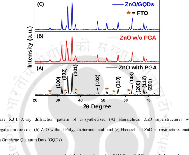
- X-ray Diffraction (XRD) Analysis
- Fourier Transform Infrared Spectroscopy (FTIR) Analysis
A smaller value of intensity ratio was achieved when hierarchical ZnO superstructures were synthesized in the presence of PGA and hexamine, specified anisotropic growth along the c-axis. The formation and presence of the different functional groups in as-synthesized graphene quantum dots was confirmed by FT-IR analysis, presented in Figure 5.3.2.
Raman Spectroscopy Analysis
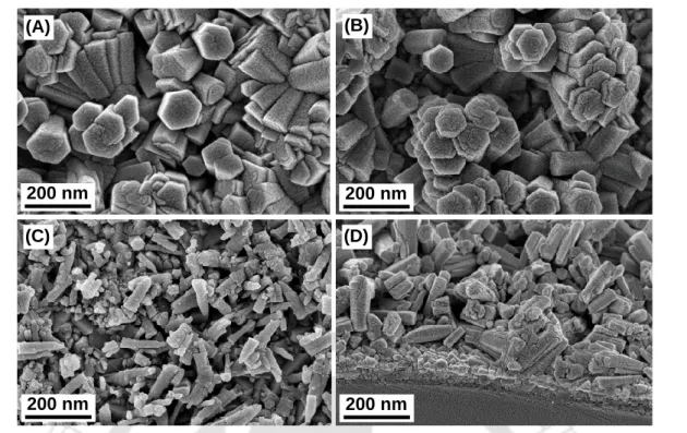
From the figure, it is clear that as the ZnO hierarchical superstructures were grown they were uniformly distributed throughout the FTO substrate. Energy Figure 5.3.4 (A) Depicts FESEM images of hierarchical ZnO superstructures synthesized at 140˚C for 4 h in the presence of polygalacturonic acid, (B) hierarchical ZnO superstructures coated with GQDs, (C) nano FESEM image of Zn -cones without using polygalacturonic acid, and (D) Cross-sectional images of as-synthesized ZnO hierarchical superstructures.
BET Surface Area Analysis
Moreover, the formation of ZnO integrated assemblies was mainly due to the anisotropic growth behavior of ZnO crystals along {0001}.
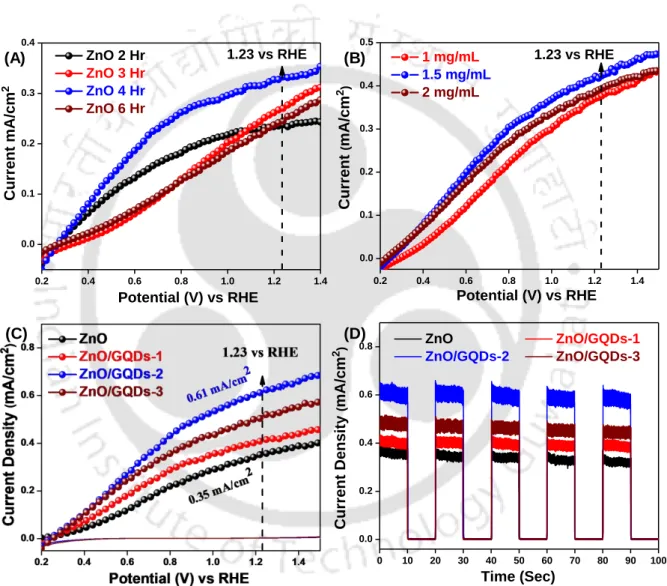
Photoelectrochemical Measurements
Based on the result, it is clear that there was a gradual increase in the photocurrent density and a maximum of 0.61 mA/cm2 was found in the case of ZnO/GQDs-2. In the case of ZnO/GQDs-3, the photocurrent density decreased and was found to be 0.51 mA/cm2.
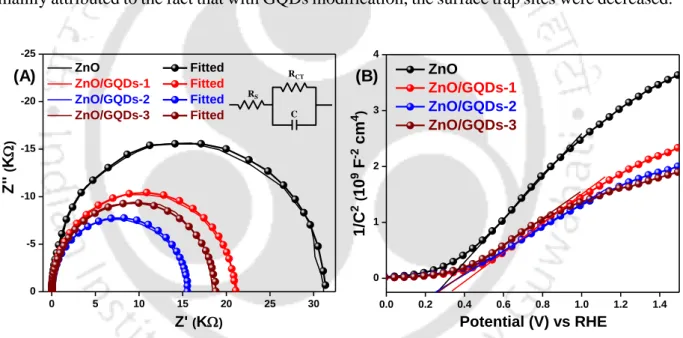
Electrochemical Impedance Spectroscopy (EIS) Analysis
To evaluate the external quantum efficiency (EQE), which is a measure of how efficiently a device converts incident light into electrical energy at a given wavelength, IPCE spectra were recorded for devices with wavelength ranges from 330 nm to 600 nm, shown in Figure 5.3. 12 (B). The equivalent circuit shown in the inset of Figure 5.3.13 (A) was used to adjust all the impedance parameters.
Charge Injection Efficiency (Hole Scavenger Test)
Faradaic Yield and Stability Measurements
Energy Figure 5.3.14 (A) Photocurrent density versus potential curves for bare and GQDs-modified hierarchical ZnO superstructures, with and without H2O2 hole trap, (B) Represents charge injection efficiencies for pristine ZnO and GQDs-modified ZnO respectively, calculated from current-density-voltage curves with and without H2O2.
Conclusions
Ultrasensitive NO X detection in simulated exhaled air: Sensing via alumina modification of in-situ grown WO 3 nanoblocks
Introduction
In particular, the precise detection of VOCs or certain gases in exhaled breath can be related to specific disease states2-7. Asthma, which is related to respiratory inflammation of the airways, is a common disease, where an increase in the concentration of nitric oxide in exhaled breath is observed.
Experimental Section
- In-situ Growth of WO 3 Structures onto Transparent Conducting Oxide
- Electrochemical Deposition of Porous -Al 2 O 3 onto the WO 3 Photoanode by Anodization
- Fabrication of Chemiresistive Device
To fabricate a two-terminal Chemiresistor device, firstly, fluorine-doped tin oxide substrates were etched with the help of HCl (Conc.) and Zn powder in order to create the active area for the sensing device.
Results and Discussions
- X-ray Diffraction Analysis
- Morphological and Structural Analysis
- BET Surface Area analysis
- X-ray Photoelectron Spectroscopy Analysis
- Sensing Studies of Chemiresistor Devices
STEM elemental analysis was used to know the elemental composition and their distribution in Al2O3 modified WO3 based device and Figure 6.3.4 represents the same. From the Barrett-Joyner-Halenda (BJH) pore size distribution plots (Figure 6.3.5), the surface area for bare and modified structures is found to be 15.3 and 28.3 m2/g, respectively.
Conclusions
This thesis outlined various aspects in the design and development of metal oxide-based photoanodic architecture to improve photoelectrochemical water splitting performance. In chapter 3 we demonstrated the idea of ternary photoanode containing a p-n heterojunction for efficient separation of photogenerated charge carriers.
LIST OF PUBLICATIONS AND
CONFERENCES/WORKSHOPS ATTENDED
Journal Articles
Mohammad Shaad Ansari, Avishek Banik, Suhaib Alam, Mohammad Qureshi, Combined effect of in-situ grown p-type CuSbS2/n-type CdS coupled with hierarchical ZnO nano-discs for enhanced photovoltaic light harvesting efficiency. Avishek Banik, Mohammad Shaad Ansari, Suhaib Alam, Mohammad Qureshi, Thermodynamic Barrier and Light Scattering Effects of Nano-Cube Assembled SrTiO3.
Conferences/Workshops