Produced phase shift gives rise to phase noise, frequency inaccuracy, spurious sidebands and increases the settling time of the PLL. The charge pump is designed with matching currents of the charge currents using the cascode current mirror and the wilson current mirror.

Working of PLL
- Phase Frequency Detector
- Charge pump and Loop Filter
- Voltage Controlled Oscillator
- Frequency divider
The charge pump circuit is used to combine both outputs of the PFD and provide a single output which feeds into the filter input. The VCO output is fed back to the PFD input through the frequency divider circuit.
![Figure 2.2.3.1 - Variation of frequency to control voltage of VCO The achievable range, ω 2 -ω 1 is called the “tuning range” [7]](https://thumb-ap.123doks.com/thumbv2/azpdfnet/10557998.0/11.918.313.605.120.350/figure-variation-frequency-control-voltage-achievable-called-tuning.webp)
Aim and Motivation
The counter will act as a frequency divider and a simple D-flip flop will act as a 2-circuit divider and these frequency dividers can be implemented by the programmable counter for accurate frequency division.
Literature Survey
Reference spurs will appear at multiples of the reference frequency and these are the most common spurs in PLLs. This will cause a phase shift, due to this shift there will be jitter in the output spectrum of the voltage controlled oscillator. Pr is the amount of spur level in dBc, Icp is the charge pump current frefis the reference frequency, R is the resistance in the loop filter, f is the full frequency, and Kvco is the gain of the VCO sensitivity.
This phase offset is introduced into the charge pump which leads to a pulse in the output spectrum of VCO. This spur occurs in a double PLL at the largest common multiple of the two comparison frequencies. Single-ended and differential-ended charge pump are the two types of charge pumps.
The gate capacitance of MI and M2 is significant when the output current of the charge pump is high and the long channel device is used for better matching. Charge pump consists of the four inputs Up, Up_b, Dn_b and Dn which are the outputs of the PFD. In the above blue color waveforms, the inputs of the charge pump are op and dn as shown in the figure Charge pump using Cascode current mirror.
The charge pump consists of the four inputs Up, Up_b, Dn_b and Dn, which are the outputs of the PFD. In the above blue color waveforms, the charge pump input is op and dn as shown in the figure Charge pump using super wilson current mirror. Surge reduction in PLL is achieved by matching currents from the charge pump.

Contibution of the Thesis
Thesis Organisation
Introduction
Excitations are induced in the PLL by periodic disturbance of the voltage-controlled oscillator from sampling at the reference frequency and due to the phase shift present in the VCO tuning line.
Spur due to leakage
Spur due to mismatchr
Non-Reference Spurs
- Auxiliary PLL Crosstalk Spur
- External Crosstalk spurs
- Fractional N Spurs
- Greatest common multiple Spurs
- Prescaler Miscounting Spurs
Crosstalk and non-crosstalk related traces are the two categories of non-reference spurs. Crosstalk-related spurting is caused by some other signal or signals affecting the output of the VCO. This spur is seen at frequency spacing from the carrier equal to the difference between the frequencies of the main and auxiliary PLLs for the dual PLLs on the board.
This boost occurs at the greatest common multiple of the two comparison frequencies comparison that corresponds to the even turning on both charge pumps at the same time. Prescaler miscalculation is caused by poor matching to the high frequency input, violating the sensitivity specifications for the PLL and VCO harmonics. Try to keep the VCO harmonics -20 dbm or lower to reduce the load on the PLL miscounting the VCO harmonics.
When a signal is transmitted and appears in the receiving Figure 2.4.2 at the IF frequency, the received signal strength is degraded due to the spur at the sidebands of the oscillator. PFD consists of the two d-Flip-flops whose D inputs are linked to logic ONE and the circuit is connected as shown above. If there is a phase difference between the input signals of the PFD, the output signals of the PFD will not be proportional to this error.
The charge pump contains two inputs which are the digital output of the PFD, according to the inputs it will provide a single output voltage using the loop filter, which is given as the tuning voltage of the VCO. The charging pump consists of two switches S1 and S2 with which pulses QA and QB are connected, respectively these pulses are the outputs of the PFD. On the PMOS side, the same situation will occur and matching this peak current is difficult as the amount of peak current varies with the output voltage.

Effect of spur on the performance of the PLL
Output spectrum of the PLL
The charge pump is a three position electronic switch which is controlled by the three states of the PFD. This configuration doubles the range of output voltage compliance compared to a single charge pump. So the average current in the charge pump is zero and in this state we can say that the PLL is in locked state.
When dn is high and up low, the voltage is reduced and the Idn current is produced, that is, the current in the charge pump is shown in a green waveform. Similarly, when up is high and dn is low, the voltage is increased and the charge pump current is increased. Charge pump with customized currents is designed using cascode current mirror and super Wilson current mirrors.
The mismatch of the charge pump currents in the cascode current mirror is 99.91 and will cause a boost of approximately 78.2 dBc. The mismatch of the charge pump currents in the Super Wilson current mirror is 99.89 and this will cause a boost of approximately 75.2 dBc. Designing the layout of the charge pump circuit and manufacturing the charge pump with reduced inducement.
9] Reduction of broadband PLLs by random positioning of charge pump current pulses Chembiyan Thambidurai and Nagendra Krishnapura.

Calculation of Spur of VCO
Introduction
It compares the phase and frequency difference between the reference clock and the feedback clock. Depending on the phase and frequency deviation, it generates two output signals "Iup" and "Idn".
Phase Detector
Dead Zone
Dead zone is a main feature of PFD phase characteristics as it introduces jitter to the PLL system. The PFD does not detect the phase error when it is within the dead zone region, so the PLL locks to a false frequency [18]. The cause of this problem is the delay time of the internal components of the flip-flop and the reset time required by the AND gate to reset both flip-flops.
When the two clocks are too close to each other (small phase error), due to the delay time of the reset delay, the UP and DOWN output signals will not be able to charge and neither output will signal leading to the loss of this small margin. Figure 4a illustrates the connection in PFDs without a dead zone, while figure 3.2.1.3 illustrates the connection in the presence of a dead zone. Many solutions have been made to this problem some of them reduce the delay time in the internal components of the PFDs, other solutions eliminate the reset path by implementing new reset techniques that will not create delay and produce PFDs quickly high.

Introduction
Simple Charge pump
Single charge pumps will only have two inputs and these inputs are connected individually, differential charge pumps have differential inputs so there will be a total of 4 inputs per charge pump. Although the single-ended charge pump has these disadvantages, they are more popular than the differential design because they do not require a dual-loop filter and offer three-state operation with lower power consumption. The charge pump can be designed with different types of switching, i.e. drain pump, gate switching and source switching pump [21].
Depending on the switching charge, the pump will have the different characteristics Switching time, power consumption, delays, costs of implementation and costs of complexity. Similarly, when QB is high, a current I dn current is drawn from the capacitor and the voltage drops. If Up is +ve and Dn is -ve, the Icp current is controlled from the Up transistor and the same current is mirrored to the capacitor due to cascode current mirror.
When Up is -ve and Dn is +ve, the current Idn is driven from the transistor Dn and the same current is mirrored from the capacitor. A Super Wilson current mirror is used in the UMP charge because it will reduce the effect of channel length. If Up is +ve and Dn is –ve, the current Icp is directed from the Up transistor and the same current is mirrored into the capacitor due to the super Wilson current mirror.
12] VLSI circuit design methodology demystified a conceptual taxonomy by Liming Xiu. 13] Charge Pump with Perfect Current Matching Characteristics in Phase-Locked Loops Jae-Shin Lee, Min-Sun Keel, Shin-I1 Lim and Suki Kim Nov 9th Phase-Locked Circuit Design, Prentice Hall.
Tyres of the charge pump
Swicthing of Charge pump
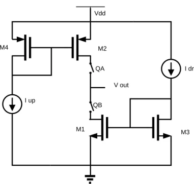
Drain switching charge pump
When QA and QB are low, the net current is zero and the V output is constant. When QA is high, the switch is close and I up current is drawn from the M2 MOS and V out increases. When the switch is on, the voltage at the drain of M1 increases by OV to the loop filter voltage held by the PLL.
Meanwhile, M1 must be in the linear region until the voltage at the drain of M1 is higher than the minimum saturation voltage. During this time high peak current is generated even though the charge coupling is not taken into account. It is caused by the voltage difference between two series starting resistors from the current mirror, M1, and the switch.
Gate switching charge pump
Source switching charge pump
Charge pump using Cascoding current mirror
Charge pump using Super wilson current mirror
Conclusion
Future work
3] Design of monolithic phase-locked loops and clock recovery circuits-a manual by Behzad Razavi Design and analysis of efficient phase-locked loop for fast phase and frequency acquisition.


