It is sold with the understanding that the publisher is not engaged in providing professional services. This work is sold with the understanding that the publisher is not engaged in providing professional services.
Introduction
A more realistic solar cell structure and model is then presented along with recombination of the conducting surface. The organic solar cell is introduced and the concepts of exciton generation and exciton decay are described in the context of heterojunction and bulk heterojunction.
Acknowledgements
Semiconductor Physics
Introduction
A fundamental understanding of electron behavior in crystalline solids is available using the band theory of solids. This theory explains a number of fundamental properties of electrons in solids, including: i) concentrations of charge carriers in semiconductors;. ii) electrical conductivity in metals and semiconductors;. iii) optical properties such as absorption and photoluminescence;. iv) properties associated with junctions and surfaces of semiconductors and metals.
The Band Theory of Solids
Satisfying the Pauli exclusion principle becomes a problem because the electrons that trade places effectively occupy new energy states extended in space. Pauli's exclusion principle can only be satisfied if these electrons occupy a series of distinct, spatially extended energy states.
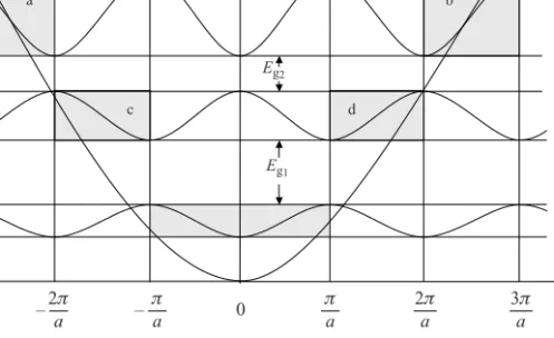
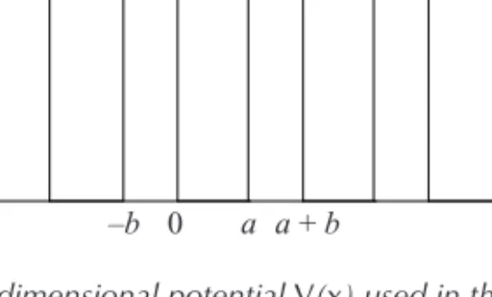
The Kronig–Penney Model
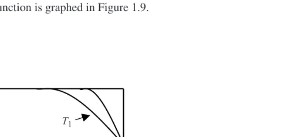
For a weak periodic potential (small P), the solutions of equation 1.4 would more closely resemble the parabola. The size of the energy gaps increases as the periodic potential increases in amplitude in a crystalline solid.
The Bragg Model
Effective Mass
To calculate m*, we start with the free electron relation E = 1. where v is the group velocity of the electron. Upon examination, Equation 1.15 actually expresses Newton's law, provided we define m Since ddk2E2 is the curvature of the plot in Figure 1.5, it is interesting to note that m* will be negative for certain values of k.

Number of States in a Band
We can apply Equation 1.16 to the free electron case where E= 2m2k2 and we immediately see that m*=m as expected. As n increases, we will inevitably reach the k value corresponding to the Brillouin zone boundary from the band model.
Band Filling
The available electronic states in the hatched regions are filled with electrons, and the energy states at higher energies are empty. For example, the group III elements Al, Ga, and In have an odd number of electrons per unit cell, resulting in the highest occupied band being half-filled, since the 2N states in that band will have only N electrons to fill.

Fermi Energy and Holes
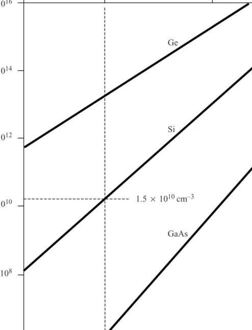
Each bond requires two electrons, and an electron can be excited across the energy gap, resulting in both a hole in the valence band and an electron in the conduction band being free to move independently of each other. In the special case of a pure or intrinsic semiconductor, we can write the carrier concentrations as ni and pi, so that ni = pi.
Carrier Concentration
This form of the density of states function applies to a box that has V =0 inside the box. The probability of the existence of a hole is 1−F (E), and from equation 1.23 we get if Ef−E kT.
Semiconductor Materials
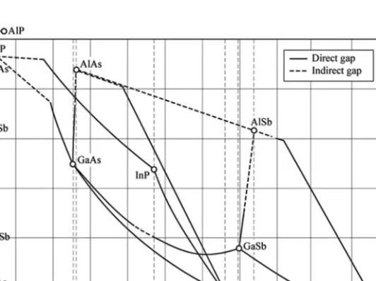
As with Group IV materials, the energy gaps of III-V semiconductors decrease as we go down the periodic table from AlP to GaP to AlAs to GaAs and to InSb. The energy gaps of II-VI semiconductors behave in the same way as illustrated by ZnSe and CdTe.
Semiconductor Band Diagrams
The degree of character of the ionic bond increases the magnitude of the periodic potential and thus the energy gap. The "A" atoms form a hexagonal close-packed (HCP) sublattice and the "B" atoms form another HCP sublattice that is offset by displacement along the vertical axis of the hexagonal unit cell.
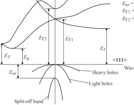
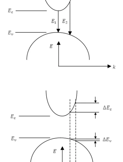
Direct Gap and Indirect Gap Semiconductors
Unlike GaAs, silicon in Figure 1.16a has a valence band maximum at a different value of k than the conduction band minimum. GaAs (Figure 1.16c), on the other hand, is a direct-gap semiconductor and has a much higher value of α (see Section 4.2).
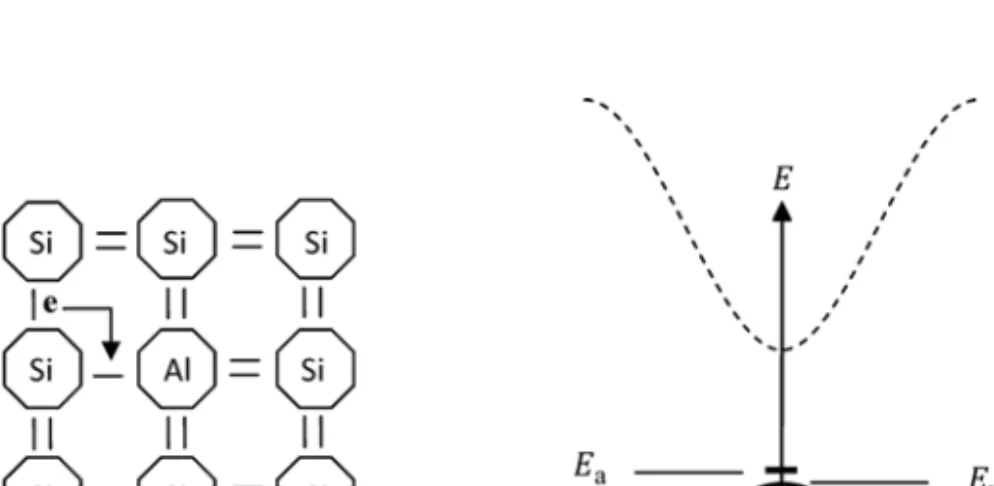
Extrinsic Semiconductors
With n-type silicon, the Fermi level will be closer to the conduction band. In p-type silicon, the Fermi level will be closer to the valence band (see Figure 1.19).
Carrier Transport in Semiconductors
To confirm the validity of Ohm's law we can start with Newton's law of motion for an electron in an electric field. The magnitude of the electric field that produces saturation effects depends on the semiconductor.

Equilibrium and Non-Equilibrium Dynamics
If Gopis constant optical generation suddenly adds a thermal generation rate with illumination starting at time t=0, the total generation rate increases to Gth+Gop. This will cause the EHP generation rate to exceed the recombination rate, and carrier concentrations will exceed equilibrium concentrations and become time-dependent.

Carrier Diffusion and the Einstein Relation
This causes the Fermi energy to occupy lower positions in the energy gap until it is close to the valence band on the right. At the same time, the tilt of the energy bands means that an electric field is present in the sample.
Quasi-Fermi Energies
Note that with brightness Fn is almost identical to the original value of Ef, but Fp moves significantly lower. This is a consequence of the large excess carrier concentration compared to the equilibrium hole concentration.
The Diffusion Equation
The hole current Ip(x=a) will be higher than the hole current Ip(x =b) due to the rate of hole recombination in the volume Adx between x =a and x =b. The latter defines the position on the x-axis where the carrier concentrations are reduced by a factor e, as shown in Figure 1.28.

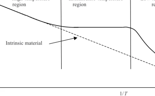
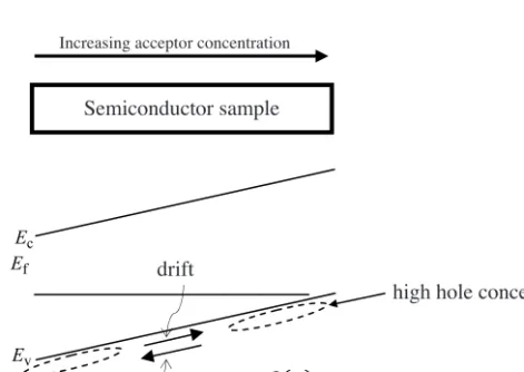
Traps and Carrier Lifetimes
There is a simple argument to assume that the trap is likely to exist at the Fermi level and near center gap. Note that at the semiconductor surface the surface gradients determine the position of the Fermi energy rather than the doping level.
Alloy Semiconductors
We can understand this transition if we consider the two conduction band minima in GaAs shown in Figure 1.16c. An additional group of III-V nitride semiconductors is shown in Figure 1.33b, and a group of II-VI semiconductors is included in Figure 1.33c.
Summary
10 cm long and has a voltage difference of 100 V from end to end, find the cross section of the rod. 1.25 (a) Find the surface recombination rate of holes on an n-type silicon semiconductor surface with the following parameters:
The PN Junction Diode
Introduction
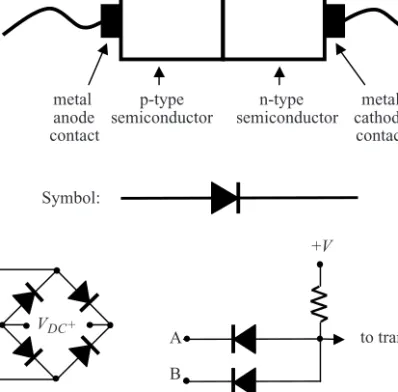
There are several basic characteristics of a diode, including the following: a) a metal anode contact attached to a p-type semiconductor forming a metal-semiconductor junction; This is achieved by gradually changing the dopant types on both sides of the semiconductor junction.
Diode Current
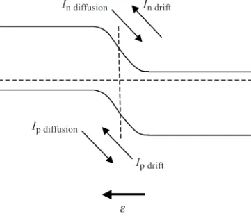
Note that in Figure 2.3 the electron and hole diffusion currents flow in the same direction and can therefore be added together in Equation 2.3 to obtain the total diode current, whereas hole and electron diffusion currents flow in opposite directions but have opposite charge polarities. This is analogous to varying the height of a waterfall in a river - the amount of water flowing down the waterfall will depend on the available flow of the water approaching the waterfall and will not be affected by the height of the waterfall.
Contact Potential
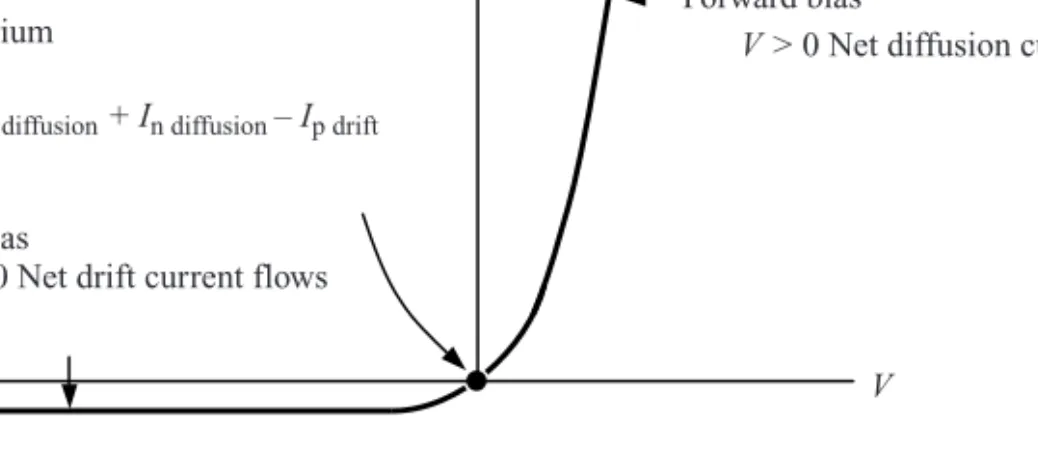
The diode current can now be plotted as a function of the applied voltage, as shown in Figure 2.7. This can also be expressed in terms of the doping levels on both sides of the junction.
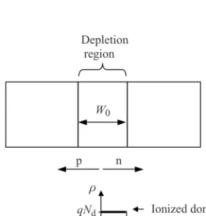
The Depletion Approximation
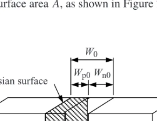
Charge densities−q Na and+q Nd (coulombs per cm3) will be respectively on the p-side and n-side of the depletion region, as indicated in Figure 2.10. Using Gauss's law we can enclose the negative charge on the p-side of the depletion region with a Gaussian surface of area A, as shown in Figure 2.11.
The Diode Equation
The limiting process involved is the recombination of the minority carriers on either side of the depletion region. The changes in carrier concentration in Equation 2.20 exist on either side of the depletion region.

Reverse Breakdown and the Zener Diode
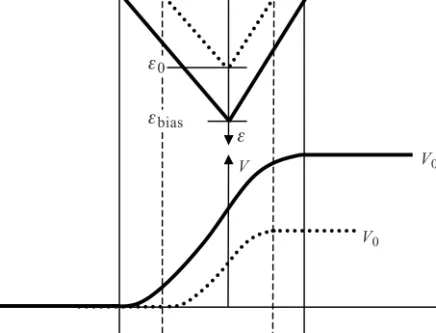
The integral of electric field across the depletion region (Equation 2.13) becomes the area under the newεversus x graph in Figure 2.19, and we obtain. This explains how the reverse current can be much larger than I0 as shown in Figure 2.18 when V exceeds the breakdown voltage Vbd.
Tunnel Diodes
At higher positive biases, electrons in the conduction band on the n-side will no longer align with the valence band on the p-side. At the Fermi energy, half of the electron states are vacant in the valence band on the p side.
Generation/Recombination Currents
In forward bias, excess carriers must actually be present in the depletion region when injected across it. Note that the hole and electron concentrations due to excess carriers are not zero in the depletion region when forward bias is applied.

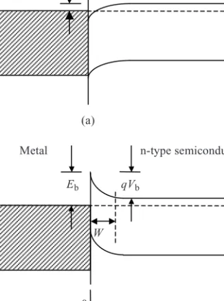
Ohmic Contacts, Schottky Barriers and Schottky Diodes
The result will be a net charge on the semiconductor and a net charge on the metal. This is the model we use for electrons in vacuum adjacent to the metal surface.
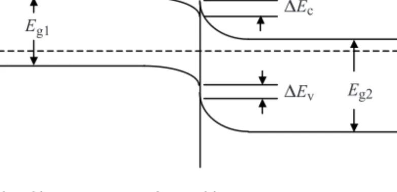
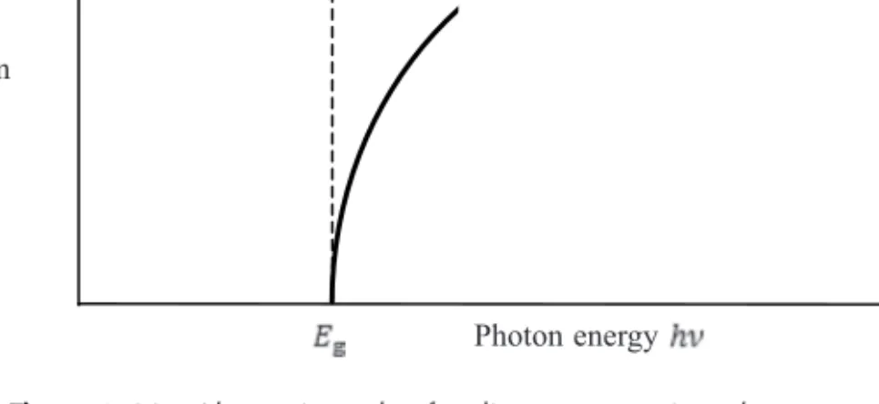
Heterojunctions
Electrons from the metal recombine with a high concentration of holes that accumulate near the surface of the p-type semiconductor. An obvious consequence of the heterojunction is the difference in the effective potential barrier for electrons and for holes.
Alternating Current (AC) and Transient Behaviour
This can be understood because in equation 2.36 a small change in the applied voltage dV causes a small change in the charge dQ near the edges of the depletion region while the width of the depletion region changes little. The second mechanism is by charge drag, in which charge flows away from either side of the depletion region spreading into the depletion region.
Summary
Use the highest field in the depletion area for this calculation. g) Find the width of the depletion region just before reverse decomposition. h). Find the capacitance of the diode at a reverse voltage of 10 volts. i) Find the voltage across the diode when the forward current is 1 A. 2.16 A sudden Si p-n junction has the following properties:.
Introduction to Luminescence and Absorption
Visible light emission is the most important wavelength range for both organic and inorganic LEDs as LEDs are widely used for lighting and display applications. Infrared (IR) and ultraviolet (UV) radiation must also be considered for both solar cells and LEDs that are not only intended to emit or absorb visible light.
Physics of Light Emission
The strongest transverse field occurs in directions normal to the direction of acceleration, as shown in Figure 3.3. Similarly, a transverse magnetic field B⊥, pointing in the direction perpendicular to the acceleration and in the radial direction, is produced during the acceleration of the charge, as shown in Figure 3.4, and is given by .

Simple Harmonic Radiator
Quantum Description
One photon of this wavelength has energy Ephoton=hc. d) Since the period of electromagnetic oscillation is Oscillation= λ. A hole-electron pair can produce one photon before being annihilated, which leads us to examine the hole-electron pair in more detail.

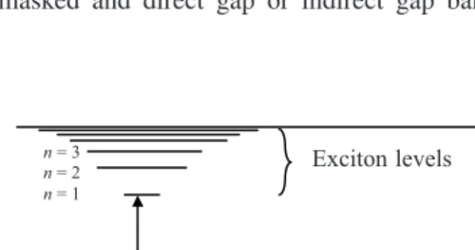
The Exciton
The exciton is not stable enough to form from scattered band states and at room temperature kT can be larger than the exciton energy levels. If an electron falls into the lowest exciton energy state corresponding ton=1, then the remaining energy available for a photon is Minimum.
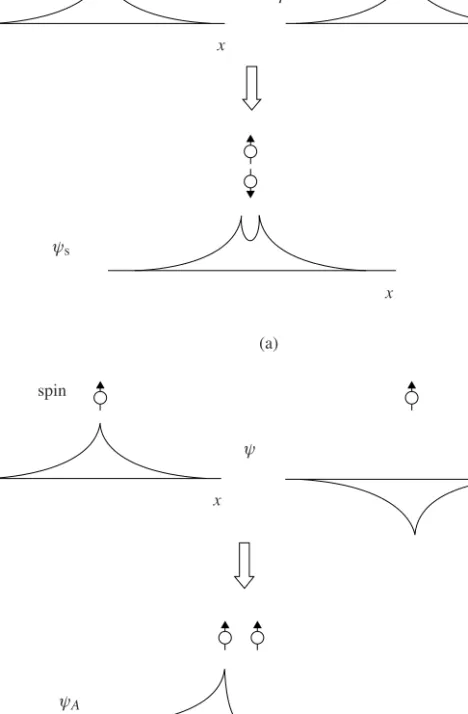
Two-Electron Atoms
If the spin part is symmetric this is a triplet state and the spatial part of the wave function must be antisymmetric. Triplet states include spin-symmetric states, meaning that the spin parts of the wave functions are symmetric.
Molecular Excitons
This prohibits a dipole transition from an excited triplet state to the ground-singlet state because the triplet state has a magnetic moment, but the singlet state does not, and the net magnetic moment cannot be conserved. In contrast, the dipole transition from an excited singlet state to the ground singlet state is allowed and strong dipole radiation is observed.
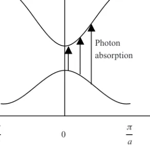
Band-to-Band Transitions
If we can determine the density of states in the joint dispersion relation, we will therefore have the density of possible photoemission transitions available in a certain energy range. We can now use the same method to determine the density of states in the joint dispersion relation in Equation 3.17 by substituting the reduced massμ into Equation 1.23.
Photometric Units
The left scale has a maximum of 1 and is referenced to the peak of the human eye response at 555 nm. The left scale is referenced to the peak of the human eye response at 555 nm.
Summary
Find the amplitude of the electron's oscillation if the radiation has the following wavelengths: How many oscillations of the electron are required to produce a phonon for each case.
The Solar Cell
Introduction
Light entering the p-n junction and reaching the depletion region of the solar cell generates. This means that the carriers must cross the depletion region and become the majority carriers on the opposite side of the intersection.
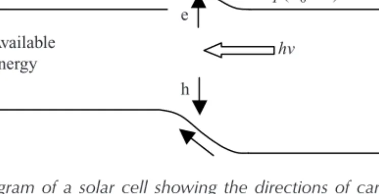
Light Absorption
In indirect-gap semiconductors, the absorption of a photon of energy hν≈Eg appears to be forbidden due to the requirement of momentum conservation, illustrated in Figure 4.4 and discussed in Section 1.12. The absorption process involving a phonon is a two-step process, as shown in Figure 4.4, along with a single-step absorption for higher energy photons.
Solar Radiation
Solar Cell Design and Analysis
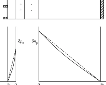
To simplify the discussion of the solar cell, we will assume that the optical generation rate G is uniform throughout the p-n junction. This means that the p-n junction can be considered to have a semi-infinite thickness as far as the excess minority carrier distributions are concerned, and in Figure 4.7 the front and back surfaces at xn=xs and xp=x are far away from the regions containing the excess carriers . .

Thin Solar Cells
If illumination were incident uniformly through the solar cell in Figure 4.10, excess carriers would be generated. These straight lines are shown in Figure 4.11 for a solar cell without illumination in a forward bias condition.
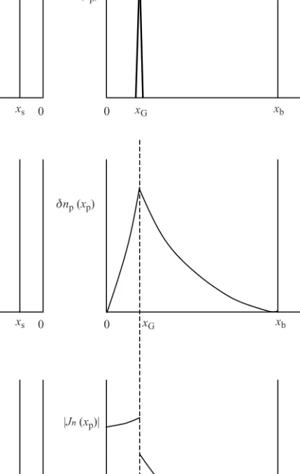
Solar Cell Generation as a Function of Depth
While some bulk recombination is always present, the reduced thickness of the solar cell would reduce recombination overall. At xp=xG there are two components of the diffusion current, both of which flow to the generation zone at xp=xG.
Solar Cell Efficiency
Much lower effective back surface recombination rates result from this and the back p+ region is therefore part of standard solar cell design. For the solar cell in example 4.1, a) Find the saturation currents at -50◦C and at +100◦C in relation to the saturation current at room temperature (300 K).