Atomic-scale research into the electronic properties of graphene use. submitted to the Graduate School of UNIST in partial fulfillment of the. requirements for the degree of Doctor of Philosophy. Here we present the atomically resolved experimental measurements of the self-assembled fullerene molecules on single-layer graphene on Cu(111).
THESIS OVERVIEW
- Carbon based materials
- Graphene
- Fullerene (C 60 )
- References
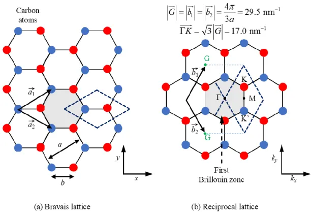
The characteristic electronic properties of graphene come from the π band and result from the overlap of pz orbitals on adjacent carbon atoms. Only the π-electrons near the Fermi level contribute to the electronic properties of graphene. a) Real space of graphene lattice (Bravais).
EQUIPMENT AND EXPERIMENTAL METHODS
Scanning Tunneling Microscopy (STM)
- Concept of STM
- Measuring Modes
STM is based on the measurement of the tunneling current between two electrodes via sample bias (or tip). The potential barrier between the tip and the sample is greater than the energy of the electrons.

Scanning Tunneling Spectroscopy (dI/dV)
These states are essentially standing wave states created between the sample and the potential barrier (tip ~ sample). Their energy depends on the shape of the tunnel barrier, which reflects the work functions of the sample and the tip.

Gundlach Oscillation (dz/dV)
During acquisition of the dz/dV spectrum, a closed feedback loop is maintained and the tunnel current is fixed. According to equation (3), if the sample bias (V) increases, the peak height also increases consistently.

STM Equipment
- Achieving UHV environment and cooling the system
- Tip Preparation
After the JT pot temperature drops below 4~4.5K, the thermal shortcut should be opened (released). JT tank temperature during (a) baking, LN2 cooling (x-axis elapsed days) and (b) LHe cooling (x-axis elapsed time).

Sample Preparation
Graphene growth methods
- CVD growth method
- STM images of CVD graphene on copper foil
- Argon-assisted growth method
To confirm monolayer graphene by comparison with a reference (see Figure 22) 49, we transferred the graphene film onto SiO2/Si(100) substrate by the following procedure (see Figure 21b). a) The surface of the graphene/copper foil is coated with poly-methyl methacrylate (PMMA). The characterization of the graphene revealed stripe patterns (Figure 26a) that have a periodicity of 1.2 ± 0.3 nm between neighboring stripes. These Moiré patterns result from the mismatches of the graphene and underlying Cu lattice (Figure 26c).
However, the square pattern mostly disappeared due to the annealing effect after graphene was treated at a high temperature, 800 ˚C. The dark spots in Fig. 26a (indicated by inverted white triangles and black dotted circle) are actually sublayer defects, not graphene or adsorbate defects on graphene, because they have almost the same electronic structure except for a slight difference in intensity compared to the neighboring region 58, 59 .After confirming the purity of the Cu(111) single crystal by STM, we used the argon-assisted graphene growth method for the UHV 65 environment.
Ethylene gas (99.8%, Sigma-Aldrich) was leaked into the preparation chamber at a pressure of Torr, followed by the introduction of argon gas to a total pressure of 1.5 mTorr, and the temperature of the substrate was maintained at 800 for 20 minutes. °C kept. min.

Evolution of electrical, chemical and structural properties of transparent and conductive chemically derived graphene thin films. Flexible, transparent, conducting films of randomly stacked graphene from surfactant-stabilized, oxide-free graphene dispersions. Atomic scale investigation of graphene grown on Cu foil and the effects of thermal annealing.
REAL-SPACE IMAGING OF THE MULTIPLE SCATTERINGS IN SINGLE
Introduction
Bena theoretically predicted that an intravalley process is possible by inserting a localized delta function impurity potential into monolayer graphene, so that Friedel oscillations (FOs) can be generated by intravalley scattering 1. However, experimentally this process was impossible on SiC(0001) due to to isolation from substrate defects with a carbon-rich buffer layer 9 , 11 , 12 . We believe that although traces of intra-valley scattering cannot appear on SLG on SiC(0001) due to its high quality 14 , intra-valley scattering may be possible with a weak substrate interaction between graphene and an impurity-rich metal surface such as Cu(111) or Au(111).
However, scattering processes for graphene on noble metal surfaces have yet to be fully investigated despite many studies. In this study, we grew graphene monolayers on Cu(111) surfaces, and investigated many scattering processes.

Experimental details
Friedel oscillation
With this definition of the work function, changes in D due to surface structure and adsorbates are responsible for changes in Φ because surface properties cannot affect EF. Thus, the probability in the allowed energy of the states relies on the following Fermi-Dirac distribution. At zero temperature, the chemical potential (µ) is equal to EF plus the potential energy per electron.
This equation, shown in Fig. 29(b), is only valid if there are many fermions in the system, so that adding one more fermion to the system has a negligible effect on µ because the Fermi-Dirac distribution is derived from the Pauli exclusion principle. Therefore, it allows at most one electron to occupy each possible state. a) Friedl oscillations near the surface and (b) Fermi-Dirac distribution for gold at three different temperatures.

Characterization of SLG on Cu(111)
However, we could not conclude whether both effective masses are the same or not, because the transmitted effective mass is directly related to the strength of the interaction between substrate and adsorbate. It also shows the surface of the Brillouin zone and the projection of the Fermi surface in this direction. This means that in the center of the surface of the Brillouin zone there are no states at the Fermi level or close to the Fermi level.
This state is confined in the direction perpendicular to the surface, but exhibits nearly free electron-like properties parallel to the surface. Surface scatterers cause variations in the local density of these states that can be easily imaged by STM. The spatial dependence of the standing waves as a function of distance is shown to indicate the sample deviations.
The wavelength of the standing waves increases as the energy is lowered relative to the Fermi level.
![Figure 30. (a) STM topographic image of [Left] graphene-covered Cu(111) and [Right] Cu(111) surface](https://thumb-ap.123doks.com/thumbv2/123dokinfo/10487864.0/71.892.167.765.171.468/figure-topographic-image-left-graphene-covered-right-surface.webp)
Results and Discussion
- Line spectroscopy (one-dimensional fast Fourier transform)
- Determination of electronic structure for single layer graphene
Momentums kx and ky are the primitive wave vectors of the graphene π-band (see, Eq. The slope of the Shockley surface state (related to effective mass) changes due to the mismatch of perpendicular direction via standing wave patterns. Therefore, a line spectroscopy does not always reflect that of the electronic structure at the Γ position, but serves as intersection lines at the K position.
Image (b) is successively divided by three different patterns, (d) graphene honeycomb structure as the top surface, (e) Moiré pattern as the interface, and (f) Cu(111) quasiparticle interference as the subsurface. e, f) One-dimensional Fourier transform results of the conductance maps in (c) and (d). Each corner of the Brillouin zone has asymmetric concentric rings, which is evidence of intervallic SLG scattering. This line is parallel to the white line in (c) which crosses the contour of constant energy circles at K± and the Γ point. e) Results of the 1D-FT conductance map in (d). g) Traces of scattering between valleys marked at point K by averaging the radius of the circles.
As noted in Figure 43, there are two circles in (d) corresponding to the surface state and the bulk electron contribution.

Conclusion
Role of pseudospin in quasi-particle interferences in epitaxial graphene investigated by high-resolution scanning tunneling microscopy. Theory of the local density of surface states in a metal: Comparison with scanning tunneling spectroscopy of an Au(111) surface. Twisted domains in monolayer graphene grown by chemical vapor deposition on Cu(111): an angle-resolved photoemission study.
Passivation of metallic surface states: microscopic origin for uniform monolayer graphene by low temperature chemical vapor deposition. Atomic-scale evidence for potential barriers and strong carrier scattering at graphene grain boundaries: A scanning tunneling microscopy study. Screening waves of steps and defects on Cu(111) and Au(111) imaged with STM: Contribution of bulk electrons.
Fourier transform line tunneling microscopy investigation of electron dispersion on the Au(111) surface as a function of energy and wave vector.
COMPETITION BETWEEN INTERMOLECULAR AND SUBSTRATE-
- Introduction
- Adsorption structures of fullerene (C 60 )
- Experimental details
- Calculation details
- Results and Discussion
- Electronic structures of C 60 on graphene/Cu(111)
- Adsorption site
- Determination of the adsorbed configuration for C 60 on graphene
- Conclusions
- References
All peak positions are directly related to the alignment of the molecular resonances of C60. This implies that self-assembled superstructure molecules on graphene exhibit different electronic structures and behaviors, depending on the supporting substrate of the graphene layer. Interestingly, all the C60 molecules have the same intramolecular configuration on graphene; the brightest region is shifted from the C-C center position and from the adsorption site at a positive bias (Figure 46(b)).
In STM topography, the intramolecular configuration is shown to be related to the electronic structure of fullerenes 22, 37. We calculated the binding energy of the C60 island without supporting layers to observe the substrate effect. Both interactions determine the individual orientations of fullerenes on graphene/Cu(111). c) Self-assembly line profiles of C60 on Cu(111) (top) and on graphene (bottom) taken along the white and red lines in (b).
Finally, we present the atomically resolved experimental measurements of the self-assembled fullerene molecules on single-layer graphene on Cu(111).

ELECTRIC FIELD-INDUCED IONIZATION OF C 60 SINGLE-MOLECULE
Introduction
Jahn-Teller effect
Results and Discussion
- Jahn–Teller effect of C 60 anion
- Making C 60 protrusion by the electric field
- Determination of charge state whether anion, cation, or neutral
- Mechanism
Fullerenes are one of the most intriguing model systems for the JTE because of their high symmetry. The weak interaction between C60 molecules and SLG/Cu(111) enables the uniform formation of C60 islands with a carbon top (CA) molecular orientation due to the competition of the strong Coulomb intermolecular and weak van der Waals interaction with SLG 43. The C60 molecules have a triangular shape orientation at this sample bias, as mentioned in the previous chapter.
As a result, we confirmed that the change in image contrast with the bias pulse is only the effect of the electric field. While the LUMO state of the protrusion and the first neighboring C60 were at a lower energy level than the neutral C60. Therefore, the C60 molecules on the Cu(111) surface could not change their shape with JTE (Figure 62).
Second, we considered that the strain energy barrier is closely related to the internal vibrational modes of the C60 molecules.

Conclusions
We investigated why fullerene molecules can be modified, what the mechanism is and how it is stable through fundamental physical theories related to the potential state of the image, ionization and the Jahn-Teller effect. Ab initio MO Study of the C60 anion radical: the Jahn-Teller distortion and electronic structure. Reversibility-controlled chemical reaction at the single molecular level in a C60 monolayer via ionization induced by a Scanning Tunneling Microscopy.
Orientation of single C60 molecules adsorbed on Cu(111): low temperature line tunneling microscopy and density functional calculations. Manifestation of dynamic Jahn-Teller distortions and surface interactions in scanning tunneling microscopy images of the C60− fullerene anion. School of Materials Science and Engineering Ulsan National Institute of Science and Technology UNIST-gil 50, B/D 104, Room #408, Ulsan 689-798 Republic of Korea.
Jung et al., “Real space imaging of multiple scattering in monolayer graphene” In progress.


