38 Figure 2.2 (a) Difference in transparency between monolayer and bilayer graphene, which reduces exactly 2.3% transparency per graphene layer [11]. 77 Figure 3.21 E-beam induced D mode of amorphous carbon. a) SEM images of amorphous carbon before and after electron beam irradiation. 79 Figure 3.23 E-irradiated amorphous carbon and SWNTs. a) SEM images before (left) and after (right) irradiation.
82 Figure 3.25 Similarity between e-beam-induced D-modes originating from amorphous carbon and SWNTs. a) Raman spectra before and after irradiation corresponding to Figure 83. Figure 3.26 Effect of irradiated amorphous carbon on the D-mode of a nanotube (left) and graphene (right). a), (c) SEM images and (b), (d) corresponding Raman spectra of the nanotube subjected to different treatments.
Carbon Nanotubes
Basic Structure
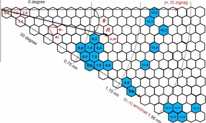
The chiral index (n, m) (m is greater than or equal to n) uniquely defines the structure of a SWNT.
Electrical and Optical Properties
- Electrical Properties
- Optical Properties
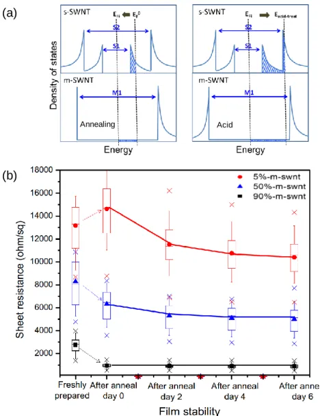
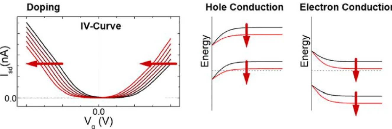
When dominated by s-SWNTs, which have different band gaps depending on chirality, contact resistance occurs because the energy gap between the Fermi level of individual SWNTs and the metal of the electrode is different [43]. However, when the ratio of m-SWNTs increases beyond 30% [55], the resistance increases rather than decreases because the tube-to-tube ratio increases. The chirality of single-walled carbon nanotubes (SWNTs) determines the density of states and results in the optical properties of SWNTs.
These peaks are caused by optical transitions, which occur due to the transition in van Hove singularities within the density of states. Depending on the chirality of the nanotubes, the wavelengths of the absorbing light are different because the energy levels are different (Figure 1.4 (b)).
Preparing CNTs on Substrate
- Chemical Vapor Deposition: General Method
- Chemical Vapor Deposition: For High Density of Nanotube
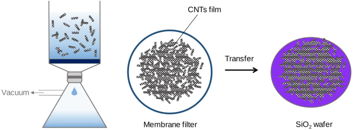
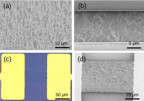
- Membrane Transfer and Amine Functionalization: Random Network Nanotubes
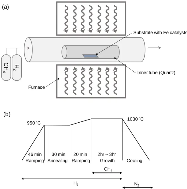
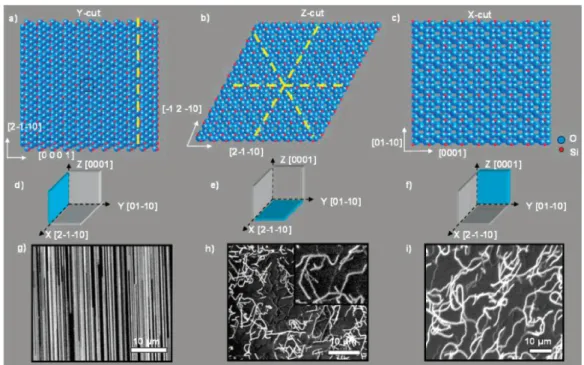
The length of the nanotubes synthesized by the CVD technique is usually in the range of micrometers to centimeters. Subsequent carbon sources are dissolved in the metal substrate and the nanotubes continue to grow in the opposite direction from the substrate. In the synthesis of nanotubes using CVD technique, the chirality of the nanotubes is determined by the catalyst size or structure.
As mentioned previously, the high-density, high-alignment nanotubes were synthesized after preannealing treatment. If a high concentration of nanotubes is required, it is preferable to disperse the nanotubes in water using a surfactant.
Graphene
Background
Electrical and Optical Properties
- Electrical Properties
- Optical Properties
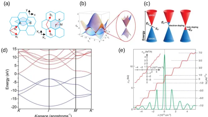
The experiment proves that the band structure of graphene actually has the cone shape shown in Figure 2.1(b) and that the mass of the charge carriers in graphene near the Dirac point is almost zero. If the temperature of the sample is lowered and the magnetic field is increased, an integer quantum Hall effect can be observed. Half of the Landau level is filled with electrons and the other half is filled with holes.
One of the other properties is that the permeability of single layer graphene is as high as 97.7%. As shown in Figure 2.4 (b), the incident light excites the electrons from the valence band into the conduction band, and the excited electrons emit light of energy that is reduced by the energy of phonons and combines with the holes created in the original valence band was formed.
![Figure 2.2 (a) The difference in transparency between single layer and double layer graphene, which reduces exactly 2.3% transparency per layer of graphene [11]](https://thumb-ap.123doks.com/thumbv2/123dokinfo/10499052.0/44.892.120.726.389.991/figure-difference-transparency-graphene-reduces-exactly-transparency-graphene.webp)
Graphene Preparation
- Exfoliated graphene
- Synthesized Graphene with Chemical Vapor Deposition
Although it is advantageous to produce graphene with large areas at low cost, the disadvantage of the liquid phase exfoliation technique is that the control of the graphene layer is difficult (Figure 2.6). The synthesis time of the carbon precursor and the ratio of gas to H2 also affect the quality of graphene. The reason is that the wavelength range reflected by the number of graphene layers changes slightly.
Synthesis of graphene by the CVD technique is one of the widely used approaches for the synthesis of high-quality and large-area graphene. To make an electrical device using CVD-growth Figure 2.9 Analysis of single-layer CVD graphene [10]. a) SEM image of graphene on SiO2/Si water.
![Figure 2.6 Graphene using liquid phase exfoliation technique [14]. (a) SEM image of initial graphite flakes](https://thumb-ap.123doks.com/thumbv2/123dokinfo/10499052.0/50.892.120.789.590.996/figure-graphene-liquid-exfoliation-technique-initial-graphite-flakes.webp)
Effect of E-Beam on Raman Spectra of Carbon Nanotube and Graphene
Effect of Low-Energy Electron Beam on Nanotubes and Graphene
- Principle of Electron Beam Equipment
- Effect of Electron Beam
- Hydrocarbon Generated by Low-Energy Electron Beam
- Defect Generated in Nanotubes and Graphene by High-Energy Electron Beam
- Debate for effect of Low-Voltage Electron Beam on Nanotubes and Graphene
- A Low-Energy Electron Beam Does Not Damage Single-Walled Carbon Nanotubes and Graphene
- Effect of Low-energy Electron Beam on Nanotube and Graphene
- Effect of Hydrocarbon on Raman Signal
- Effect of Amorphous Carbon on Raman Signal
- Experimental
- Conclusion
This means that the hydrocarbon was deposited thinly and thickly at the high voltage of the electron beam. In addition, as the current of the electron beam increases, the width of the hydrocarbon increases. When the PMMA film was removed using acetone, the hydrocarbon was transferred to the nanotubes that had not been exposed to an electron beam.
The D mode in the Raman spectra was not enhanced by the nanotubes, which were contacted by hydrocarbons without receiving electron beams. Therefore, I need to check that the electron beam-induced D-mode appears from the hydrocarbon-contacted nanotube without receiving the electron beam. However, the electron beam-induced D-mode was seen even if the PMMA was removed and the hydrocarbons were not in the irradiated nanotube.
When the electron beam irradiated PMMA film was removed using acetone, the cross-linked PMMA remained in the irradiated area of the electron beam. The beam was first irradiated on the nanotube and covered with PMMA film, and the D mode induced by the electron beam disappeared. In summary, it is inevitable that the hydrocarbon is deposited on the exposed part of the electron beam.
So there is even more doubt that the electron beam-induced D-mode originates from amorphous carbon. In the Raman spectra, I found the electron beam-induced D state that was not present in the pristine nanotube. When the amorphous carbon was removed through the annealing process, the electron beam D state was found to be reduced.
In other words, the removal of amorphous carbon during the annealing process also reduces the electron beam. The D-mode was enhanced by an electron beam from amorphous carbon and this amorphous carbon was on the surfaces of nanotubes and graphene.
Effect of Surface Properties on Sensitivity of Gas Sensor Using Carbon Nanotube and Graphene
Carbon Nanotube-based Gas Sensor with Functionalization
- Background
- Sensing Mechanism of Nanotube-Based Gas Sensor
- Non-Covalent Functionalization
- Functionalization with Covalent Chemistry
- Functionalization with Plasma Treatment
- Difficulty of Plasma Functionalization with Powdery Materials
- Nanotube Functionalization with Plasma Treatment
- Effect of Circulation on Uniformity of Functionalization
- Gas Sensor with Plasma-Treated CNTs
- Experimental
- Conclusions
In general, nanotubes are known to have p-doping properties because oxygen molecules are physically adsorbed on the nanotube surface under ambient conditions. Non-covalent functionalization is advantageous in that the electrical properties of the nanotubes do not change significantly because the coating material is only adsorbed on the surface of the nanotubes. Another approach is to use a strong acid to create a defect in the nanotube sidewall for covalent functionalization.
In the next chapter, I study the regulation of functionalization and functionalization of CNTs using plasma functionalization. If the nanotubes are not uniformly functionalized on the nanotube surface, the interface of the nanotube matrix is not uniform and thus the structure is weakened. It is also an additional problem that the phenomenon of the powder is stacked on the wall of the plasma actuator, and the lines should be aligned on the plasma.
The increase in the ratio of the oxygen element means that the ratio of oxygen functionalization increases. In the mechanism, radicals in the oxygen/air plasma create defects on the surface of the nanotubes and attack carbon-carbon double bonds. Normally, when the plasma is generated using oxygen gas, carboxyl groups or hydroxyl groups are formed on the surface of the nanotubes.
When there is no repeated circulation, the degree of MWCNTs functionalization is not homogeneous, and the functionalization of MWCNTs will depend on the depth of the electrode [205, 206]. The D-state on the wall of the nanotube is increased and this D-state means the degree of functionalization. As the functionalization proceeded, the surface of the nanotube was damaged and the carbon–carbon double bond was reduced.
Preparation of chemical vapor deposition-synthesized graphene-based gas sensors with high
- Importance of CVD technique
- Effect of CVD Synthesis Process on Graphene Properties
- Background of Graphene-Based Gas Sensor
- Effect of CVD Synthesis Process on Sensitivity
- Effect of Air Annealing on Graphene Surface
- Experimental Condition
- Conclusion
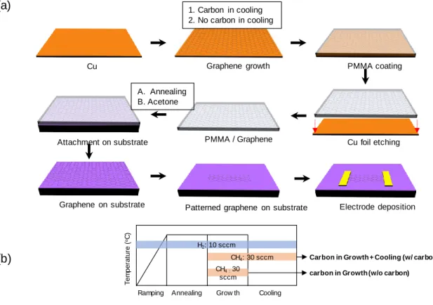
In the case of graphene without releasing carbon precursor in the cooling process, without carbon &. In the case of no-carbon and annealed graphene, grain boundaries were not clear in AFM analysis. The grain boundaries were found in both the no-carbon and annealed graphene and the no-carbon and acetone graphene.
The I2D/IG intensity ratio of the 2D band (2700 cm−1) and the G band provides information about the graphene layers. After E-beam lithography, a resist residue remains on the surface, which increases the sensitivity of the graphene. The graphene without carbon and acetone was also sensitive to 5 ppm DMMP, but less sensitive than carbon + annealing graphene.
However, the sensitivity of carbon-free and annealed graphene is very low compared to that of exfoliated graphene. After air annealing, the noise intensity decreased significantly with carbon and annealed graphene and showed a response to 5 ppm DMMP. Carbon- and acetone-free graphene improved the response after air annealing but did not reduce the noise intensity.
However, it was shown that the ΔR/R0 after air annealing was relatively uniform in graphene synthesized under the w/o carbon & annealing conditions. The w/carbon and acetone graphene showed the clearest difference in response and S/N before and after air annealing. Study showed that the sensitivity of graphene increased when the width of the graphene was narrower [234].
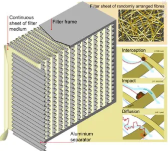
Estimation of Residual Life of Gas Filtration System
- Background
- Air Filter for Small Particles
- Activated Carbon Filter for Small Molecule
- Estimation of Residual Life of Gas Filtration System
- Conclusion
- Conclusion
Lu, et al., “Using nanoscale thermocapillary flows to create arrays of semiconducting single-walled carbon nanotubes,” Nature Nanotechnology , vol. Du, et al., "Microwave cleaning of horizontally aligned large-area arrays of single-walled carbon nanotubes," Nature Communications, vol. Alam, et al., "High-Performance Electronics Using Dense, Perfectly Aligned Arrays of Single-Walled Carbon Nanotubes," Nature Nanotechnology, vol.
Dai, et al., “Near infrared imaging and photothermal ablation of vascular inflammation using single-walled carbon nanotubes,” Journal of the American Heart Association, vol. Xu, et al., "Chirality-Specific Growth of Single-Walled Carbon Nanotubes on Solid Alloy Catalysts," Nature, vol. Hong, et al., “Stretchable graphene transistors with printed dielectrics and gate electrodes,” Nano Letters, vol.
Lee, et al., "Graphene oxide thin films for flexible non-volatile memory applications," Nano Letters, vol. Myung, et al., "Sensitive detection of H2S using gold nanoparticles decorated single-walled carbon nanotubes," Analytical Chemistry, vol. Rutledge, et al., "Modular Functionalization of Carbon Nanotubes and Fullerenes," Journal of the American Chemical Society, vol.
Luo, et al., "p-Hexafluoroisopropanol phenyl covalently functionalized single-walled carbon nanotubes for the detection of nerve agents," Carbon, vol. Yu, et al., “Single-walled carbon nanotubes with CuO networks for gas sensing,” Journal of Materials Chemistry C, vol. Hierold, et al., "Spatially resolved Raman spectroscopy of single- and few-layer graphene," Nano Letters, vol.
![Figure 2.5 An illustrative procedure for mechanically exfoliated graphene using Scotch-tape [8]](https://thumb-ap.123doks.com/thumbv2/123dokinfo/10499052.0/49.892.132.762.623.987/figure-illustrative-procedure-mechanically-exfoliated-graphene-using-scotch.webp)
![Table 1 Carbon solubility and growth mechanism using various metal for CVD graphene [7]](https://thumb-ap.123doks.com/thumbv2/123dokinfo/10499052.0/51.892.111.784.734.892/table-carbon-solubility-growth-mechanism-using-various-graphene.webp)
