efficiency of metal halide perovskites by examining luminescence-limiting factors
Cite as: APL Mater. 8, 020904 (2020); https://doi.org/10.1063/1.5136308
Submitted: 12 November 2019 . Accepted: 14 January 2020 . Published Online: 13 February 2020 Hyun Myung Jang, Joo-Sung Kim, Jung-Min Heo, and Tae-Woo Lee
ARTICLES YOU MAY BE INTERESTED IN
Performance boosting strategy for perovskite light-emitting diodes
Applied Physics Reviews 6, 031402 (2019); https://doi.org/10.1063/1.5098871 Metal halide perovskites for blue light emitting materials
APL Materials 8, 040907 (2020); https://doi.org/10.1063/1.5144101
Polymer–perovskite blend light-emitting diodes using a self-compensated heavily doped polymeric anode
APL Materials 8, 021101 (2020); https://doi.org/10.1063/1.5140519
Enhancing photoluminescence quantum efficiency of metal halide perovskites
by examining luminescence-limiting factors
Cite as: APL Mater.8, 020904 (2020);doi: 10.1063/1.5136308 Submitted: 12 November 2019•Accepted: 14 January 2020• Published Online: 12 February 2020
Hyun Myung Jang,1,a) Joo-Sung Kim,2 Jung-Min Heo,2 and Tae-Woo Lee1,2,3,b) AFFILIATIONS
1Research Institute of Advanced Materials, Seoul National University, 1 Gwanak-ro, Gwanak-gu, Seoul 08826, South Korea
2Department of Materials Science and Engineering, BK 21 PLUS SNU Materials Division for Educating Creative Global Leaders, Seoul National University, 1 Gwanak-ro, Gwanak-gu, Seoul 08826, South Korea
3Institute of Engineering Research, Nano Systems Institute (NSI), Seoul National University, 1 Gwanak-ro, Gwanak-gu, Seoul 08826, South Korea
a)E-mail:[email protected]
b)Author to whom correspondence should be addressed:[email protected]
ABSTRACT
Metal halide perovskites (MHPs) show superior optoelectronic properties, which give them the great potential for use in next generation light-emitting diodes (LEDs). In particular, their narrow emission linewidths can achieve ultrahigh color purity. However, the reported lumi- nescence efficiency (LE) values are not high enough to be commercialized in displays and solid-state lightings. Moreover, the operational stability of LEDs associated with the overshooting of luminance and the high relative standard deviation of reported external quantum effi- ciencies are still problematic. In this perspective, we review photophysical factors that limit the photoluminescence quantum efficiency of perovskite-based LEDs. These factors are categorized into (i) weak exciton binding, (ii) nonradiative recombinations, (iii) slow cooling of long-lived hot carriers, (iv) deep-level defects, and (v) interband transition rates. We then present various physicochemical methods to effec- tively overcome these luminescence-limiting factors. We finally suggest some useful research directions to further improve the LE of MHP emitters as core components in displays and solid-state lightings.
© 2020 Author(s). All article content, except where otherwise noted, is licensed under a Creative Commons Attribution (CC BY) license (http://creativecommons.org/licenses/by/4.0/).https://doi.org/10.1063/1.5136308., s
I. INTRODUCTION
Metal halide perovskites (MHPs) are promising semiconduct- ing materials for next generation optoelectronic devices. MHPs show superior electrical and optical properties, which give them great potential for use in light-emitting diodes (LEDs).1–4In par- ticular, their narrow emission linewidths [with a full width at half- maximum (FWHM) of≤20 nm] can achieve ultrahigh color purity (color gamut ≥140% in NTSC standard). These are superior to the properties of organic emitters (FWHM>40 nm; color gamut
<100% in NTSC standard) and inorganic quantum dot (QD) emit- ters (FWHM ≈ 30–40 nm; color gamut ≈120% in NTSC stan- dard).5Three-dimensional (3D) polycrystalline MHPs have ABX3- type crystal structure, where A is an organic or inorganic cation
that functions as a structural template, B is a metal cation, and X is a halide anion.6,7Each B-site atom is surrounded by six X atoms, and each A-site cation or molecule is positioned in the center of BX6octahedral frameworks. To be structurally stable, polycrystalline MHPs should have the tolerance factor,t=√(r2(rA+rX)
B+rX), whereris the ionic radius, in the range 0.8≤t ≤1.0, and the octahedral factor (μ=rB/rX) in the range 0.44≤μ≤0.9.7–9
3D polycrystalline MHPs were first chosen for use in light emitters for perovskite-based LEDs (PeLEDs) because of the advan- tages of simple synthesis, easy film fabrication, and effective charge- transporting properties.2–4,10 In 2014, the bright PeLEDs with a brightness of∼400 cd/m2at room temperature had been developed using 3D polycrystalline MAPbX3-based MHP emitters by adopting
simple planar structures,2,3where MA denotes a CH3NH3organic cation. These PeLEDs had solution-processed MHP emitting lay- ers between charge-transporting organic layers with electrodes.2,3 The electroluminescence efficiencies of the early-stage PeLEDs in 2014 are (i) infrared (IR) radiance of 13.2 W/(sr m2) and external quantum efficiency (EQE) of 0.76% for MAPbI3−xClxand (ii) lumi- nanceL= 417 cd/m2and EQE of 0.125% for MAPbBr3.2,3 These are inferior to those of conventional organic light-emitting diodes (OLEDs) and lag far behind the commercially required performance.
However, those solution-processed PeLEDs clearly proved the pos- sibility of room-temperature processed next-generation LEDs with a high color purity of a narrow FWHM of ≈20 nm2,3 and flex- ible LED devices.3 The first efficient PeLEDs with EQE of 8.53%
(42.9 cdA−1) similar to the level of OLEDs have been reported by making small nanograin films using additive-based nano-crystal pinning processes in 2015.4 Since then, EQEs of PeLEDs have fur- ther been improved to demonstrate that PeLEDs are promising next-generation LEDs.4,11–15
Recently achieved EQEs of ∼20% clearly show the possi- bility of 3D MHPs as next-generation light emitters.16–19 An island/lid-stacked structure (termed quasi-core/shell) of polycrys- talline CsPbBr3capped with MABr additive yielded EQE of∼20%
[current efficiency (CE) = 65 cd/A] in green polycrystalline PeLED.16 This structure allowed a high photoluminescence quantum yield (PLQY). An increase in light extraction efficiency in polycrystalline PeLEDs based on submicrometer-scale FAPbI3 (FA = formami- dinium) yielded the maximum EQE of 20.7% (the minimum EQE of 17.75% and average EQE of 19.2% with the relative standard deviation of 4%) with invisible IR emission.17The increase in light extraction from FAPbI3was achieved using an insulating layer of 5-aminovaleric acid (5AVA) to reduce leakage current through the uncovered emitter region and to passivate surface defects.17These rapid developments of PeLEDs have confirmed their possibility of utility as the next-generation emitters. However, the reported lumi- nescence efficiency (LE) values are still lower than those of OLEDs that are commercialized in displays and solid-state lightings. More- over, the high relative standard deviation of the reported EQEs is problematic. Therefore, it is of great importance to develop a reliable method of producing high-efficiency PeLEDs with a narrow EQE distribution.
In this perspective, we review photophysical factors that strongly affect the photoluminescence quantum efficiency (PLQE) of MHP-based PeLEDs. These factors are classified as (i) weak exci- ton binding in MHPs, (ii) nonradiative recombination of charge carriers, (iii) slow cooling of long-lived hot carriers, (iv) deep-level defects and ion migration, and (v) interband transition rates. By theoretically examining these points, we present various physico- chemical methods to overcome the luminescence-limiting factors and finally suggest several research directions to further improve the LE of MHP emitters as core components in displays and solid-state lightings.
II. LUMINESCENCE-LIMITING PHYSICAL FACTORS A. Weak exciton binding in MHPs
The electroluminescence (EL) efficiency of PeLED is most strongly affected by charge-carrier recombination processes and
concomitant photoluminescence quantum efficiency (PLQE) of MHP emitters. Charge-carrier recombination in MHP emitters occurs in several steps [Fig. 1(a)]: Photo-illumination does excite the electrons from the valence band maximum (VBM) into conduction band minimum (CBM) and, subsequently, form electron–hole pairs, excitons (process 1). Some of these pairs recombine with each other and emit light, called “radiative recombination of electron–hole (e-h) pairs” or “unimolecular excitonic recombination” (process 2.1). Other pairs separate into free-charge carriers (process 2.2).
Excited electrons and holes can experience an energetically stabilizing Coulombic attraction, forming electrostatically neutral quasi-particles, called excitons.20The ratio of the radiative recom- bination of e-h pairs to the separation into free-charge carriers (defined asRREC) is determined by the exciton binding energy (Eb) which defines the energy needed to separate the bounde-hpairs,20
Eb= μ 2̵h2( e2
4πεoεr)
2
=RH
μ
moε2r = e2 8πεoεraB
, (1)
where RH(=13.6 eV) is called the Rydberg constant and denotes the binding energy of electron in the ground-state 1s orbital of the hydrogen (H) atom; mo is the mass of a free electron;
μ[≡ (m1e+m1
h)−1]is the reduced mass of charge carriers, whereme
andmh, respectively, denote the effective mass of an electron and that of a hole; andεris the relative dielectric permittivity of MHPs.
The aB term in the last expression of Eq. (1) denotes the exci- ton Bohr radius (=4πεoεr̵h2/μe2) and roughly represents the aver- age distance between the electron and the hole in a given exciton (e-hpair).
MHPs have low and similar effective masses (me ≈0.15mo; mh≈0.14mo) and are ion-bonded crystals, so electrons and holes can freely move, rotate, and oscillate in the MHP crystals. As a result, the reduced mass of ane-hpair is as small as 0.072mo, as obtained by μ ≡memh(me + mh)−1. On the other hand, heavy- metal atoms (e.g., Pb) and orientational motion of the A-site organic cations21 in MHPs prevent the movement of charge carriers and induce screened Coulomb interaction, thereby leading to largeεr
and polarization. SinceEbis proportional toμbut is inversely pro- portional to the square of εr [Eq. (1)], the observed small exci- ton binding energy of MHPs is mainly caused by small reduced mass (μ) and large dielectric permittivity (εr). As a result,Eb val- ues of 3D MHPs are significantly smaller than 100 meV, 30–50 meV in MAPbI3and∼76 meV in MAPbBr3,22,23similar to the thermal energy per atom at room temperature (kBT= 25.7 meV). TheseEb
values were obtained by various experimental methods, including magneto-optical absorption spectroscopy,22 optical absorption,24 and temperature-dependent PL.25In MHPs,RRECcan be estimated by applying the Saha–Langmuir equation,26
n⋅x2 1−x =n2FC
nexc= (2πμkBT
h2 )3/2e−Eb/kBT, (2) wherenexcdenotes the density ofe-hexciton pairs,nFCis the den- sity of free-charge carriers, xdenotes the fraction of free carriers over the total density of exciton (=nFC/n),μis the reduced mass of the exciton, andnis the total density of excitation (=nFC +nexc).
3D MHPs with small Eb values (30–76 meV)22,23 have dominant
FIG. 1. Recombination mechanisms, kinetics, and photoluminescence effi- ciency of charge carriers. (a) Schematic illustration describing various recombi- nation mechanisms of charge carriers in MHPs. The four major recombination pathways are excitonic recombination (∝n1), trap-assisted recombination (∝n1), bimolecular recombination (∝n2), and Auger recombination (∝n3).
(b) The free-charge fraction (x) plotted as a function of the total density of excitation (n) at three different exciton binding energies. The present plot is based on Eq. (2) for the charge carriers in thermal equilibrium at room temperature. Reproduced with per- mission from D’Innocenzoet al. Nat.
Commun. 5, 3586 (2014). Copyright 2014 Nature Publishing Group. (c) Recombination pathways of excited charge carriers in 3D bulk MHPs:
dissociated into free-charge carriers and then trapped in defect states or recombined to emit light. Reproduced with permission from Xing et al. Nat.
Commun.8, 14558 (2017). Copyright 2017 Nature Publishing Group. (d) The calculated PLQE curves for variousk1
values, all showing a peak in the PLQE at the characteristic charge-carrier density, (k1/k3)1/2. The calculated result shows that for fixed k2 (bimolecular recombination constant) andk3(Auger recombination constant), the PLQE increases rapidly with decreasing k1 (trap-mediated recombination constant).
(e) The calculated PLQE curves for vari- ousk2values. Sincek1andk3are fixed, all curves exhibit their peaks at the same charge-carrier density (np), namely,np
= (k1/k3)1/2= 3.16×1017 cm−3. The result shows that for fixedk1 and k3
rate constants, the PLQE increases with increasingk2. Reproduced with permis- sion from Xinget al.Nat. Commun.8, 14558 (2017). Copyright 2017 Nature Publishing Group.
free-charge carriers at room temperature. RREC [≡nexc/nFC = (n
−nFC)/nFC], which is approximately inversely proportional to the free-charge fractionx(=nFC/n), increases gradually with increasing Eb [Fig. 1(b)] or decreasing temperature26 for a given total den- sity of excitation (n =nFC +nexc). The n-dependent x shown in Fig. 1(b) follows the above Saha–Langmuir equation. This direct dissociation of electron–hole pairs into free-charge carriers has stim- ulated research into MHP-based solar cells but has impeded the development of MHP-based LEDs because efficient light emission in PeLEDs requires strongly bound electron–hole pairs.
One very efficient approach to overcoming this obstacle in PeLEDs is controlling the physical dimension and dimensionality of
MHPs. Decreasing the physical dimension from micrometer scale to nanometer scale in 3D perovskites greatly improves the LE of PeLEDs because reducing the particle dimension leads to the con- finement of charge carriers and, consequently, enhances the rate of radiative recombination of electron–hole pairs (excitons) within a nanograin.4,13,27Similarly, strong excitonic absorption and lumi- nescence features are observed at room temperature in layered lead halide perovskites,28withEbvalues as high as∼300 meV for typ- icaln= 1 Pb–I materials, where “n” is the number of octahedral layers that make up a single slab in layered halide perovskites.
The strong excitonic character of the layered 2D perovskites com- pared to their 3D congeners29results from the cooperative effects
of quantum and dielectric confinement.28Despite some differences between the layered perovskites and true quantum-well systems, these two effects, which apply to quantum wells, qualitatively explain the greatly enhancedEbin 2D perovskites.28,30
In an electronically 3D material, such as (CH3NH3)PbI3, the excitonic wavefunctions are similar to the 3D hydrogenic wave- functions of the Bohr model.20 In 2D systems, dimensional con- finement of the wavefunction leads to a 4-fold enhancement of Ebrelative to its 3D congener through quantum confinement.28,31 On the other hand, dielectric confinement results from relatively poor screening of the Coulombic attraction between the electron and hole32,33by the organic layers that are significantly less polar- izable than the inorganic layers.30 The polarizability (αE) of the halide ion seems to affectEbas lead iodide perovskites exhibit lower Ebvalues than lead bromide perovskites, e.g.,Ebof∼220 meV for (PEA)2PbI4vsEbof∼356 meV for (PEA)2PbBr4, owing to greatly enhancedαEof I, as compared withαEof Br.34,35Here, PEA stands for phenylethylene ammonium. It is now known that the reduc- tion of both Eb (by reducing both dielectric and quantum con- finements) and the bandgap (Eg) can be achieved by increasing the thickness of the inorganic layers. The n = 1 member of the (C6H5(CH2)2NH3)2(CH3NH3)n−1PbnI3n+1family [i.e., (PEA)2PbI4] hasEgandEbvalues of 2.58 eV and 0.220 eV, respectively, while the n = 2 perovskite has corresponding values of 2.34 eV and 0.170 eV, respectively,34,36which leads to a red shifting of the luminescence withn, converging toward the emission energy of the n=∞ 3D perovskite, (CH3NH3)PbI3, at 1.60 eV.
B. Nonradiative recombination processes of charge carriers
Let us now examine the recombination kinetics of charge car- riers in MHPs to quantitatively address the effects of nonradiative recombination processes on the suppression of LE. Photoexcited charge carriers that separate into free charge carriers (process 2.2) can subsequently undergo one of the following three steps: bimolec- ular radiative recombination (process 2.2.1), or trapping into deep- level defect states, followed by the Shockley–Read–Hall (SRH) non- radiative recombination (process 2.2.2), or recombination by multi- particle interaction, and typically by three-body Auger recombina- tion (process 2.2.3). Then, one can write the following equation for the recombination kinetics of charge carriers:37
dn(t)
dt = −k1n−k2n2−k3n3, (3) wheren(t) is the charge-carrier density at timet,k2is the rate con- stant for the bimolecular recombination of free-charge carriers, and k3denotes the rate constant for the trimolecular Auger recombina- tion process. On the contrary, two distinct rates contribute tok1, namely,k1=k1(exc)+k1(def), wherek1(exc) represents the rate con- stant for the unimolecular excitonic recombination (process 2.1) and k1(def) denotes the rate constant for the defect-mediated nonradia- tive recombination (process 2.2.2). Recombination rates of MHPs can be obtained by fitting the transient-absorption kinetics data for different pump fluences: 3D MAPbBr3films showedk1≈27.2μs−1 (i.e., 27.2 × 10⁶ s−1), k2 ≈ 4.9 × 10⁻¹⁰ cm3 s−1, and k3 ≈13.5
× 10−28 cm6 s−1, and 3D MAPbI3 films showedk1 ≈72.7μs−1, k2≈1.5×10⁻¹⁰cm3s−1, andk3≈3.4×10⁻²⁸cm6s−1.38In MHPs,
k2andk3are inherent values, whereask1is affected by the degree of charge-carrier confinement and by defect density. This indicates that specific recombination pathways in 3D MHPs can be controlled by tuning defect density, crystallinity, and dimensionality or physical dimension of MHP crystals.37
According to the above kinetic data, for both 3D MAPbBr3and MAPbI3films,k1andk2nare much greater thank3n2for the charge- carrier density (n) up to 1017 cm−3. Since a typical charge den- sity under LED operating conditions isn≤1015cm−3, the charge- recombination rate due to the trimolecular Auger process (−k3n3) is negligible as compared with the other two contributions (−k1nand
−k2n2). Under this condition, one can obtain the following solution for Eq.(3)after some mathematical manipulations:
n(t) = k1e−k1t k2{(1−e−k1t)+n1
o(kk12)}, (4)
wherenodenotes the charge-carrier density att= 0 (initial photoex- citation density). In the initial stage of the transient PL decay,n(t) can be approximated as
n(t) = noe−k1t
{1 +k2not}. (5) Thus, at a low value ofno, plotting lnn(t) with respect tot(time after excitation) yields a single straight line with the slope being−k1in the initial stage of decay. With increasingno, a linear plotting is no more valid. Instead, we havedlnn(t)dt = −k1−{1+kk22nnoot}. Thus, the magnitude of the initial slope of PL decay (ast→0) increases with increasing no. This prediction does accord well with the measured transient PL decay curves with different initial photoexcitation densitiesno.39
In conventional polycrystalline 3D MHPs with large grains, Eb is small, so most electron–hole pairs dissociate directly into free-charge carriers, suppressing the unimolecular excitonic recom- bination (k1) at room temperature. In view of this, the bimolec- ular recombination of free-charge carriers is the main radiative mechanism in conventional polycrystalline 3D MHPs with large grains at room temperature [Fig. 1(c)]. Therefore, the photolumi- nescence quantum yield (PLQY) or efficiency (PLQE) in MHPs can be represented as40
Φ(n) =(dn/dt)rad
(dn/dt) = k1(exc)+k2n
k1(exc)+k1(def)+k2n+k3n2, (6) where (dn/dt)r adand (dn/dt) denote the radiative and total recom- bination rates, respectively. Under low excitation fluences (charge- carrier density of <1015 cm−3 in LED operating conditions), the defect-mediated nonradiative recombination of charge carriers [k1(def)] dominates radiative recombination mechanisms, i.e., the unimolecular recombination of excitons [k1(exc)] and the bimolec- ular recombination of free-charge carriers [k2n] in 3D MHP films.
The PLQE then increases with increasingndue to the gradual dom- ination of the second-order bimolecular recombination over the first-order charge-carrier trapping. At higher carrier densities, where the three-particle Auger recombination becomes effective and dom- inates the bimolecular recombination, the PLQE will then decrease with increasingn. This decrease in the PLQE can be attributed to a nonradiative nature of multicharge carrier interactions such as Auger and biexciton recombinations.37 Sincek2(∼10−10 cm3s−1)
and k3 (∼10−28 cm6s−1) are the intrinsic parameters for a given MHP,41,42one should maximize the unimolecular excitonic recom- bination rate [k1(exc)] for obtaining an enhanced PLQE [Eq.(6)].
This goal can be achieved either by the dimensional confinement of charge carriers using nano-sized grains in 3D MHPs4,13 or by increasing the exciton binding energy (Eb) in quantum-confined quasi-2D perovskites27,43–46 (see Sec. III B). On the other hand, Eq. (6) also predicts that the trap-mediated recombination rate [k1(def)] should be minimized for achieving an enhanced PLQE.
If the bimolecular recombination rate [k2] is significantly higher than the recombination rate of excitons [k1(exc)], one can expect a peak in then-dependent PLQE as the following inequal- ity is established under this condition:37k2n2≫k1(exc)n≈0. Then, the peak PLQE [Φp(n)] can be obtained by imposingdΦ(n)/dn= 0 and is given by
Φp= 1
1 + 2(k1k3)1/2k−12 , (7) where the charge-carrier density at the peak is given by np
= (k1/k3)1/2. This relation is valid for the trap-mediated recombi- nation only,37 wherek1≈k1(def). The calculated PLQE curves for variousk1values all show a peak in the PLQE at the characteristic charge-carrier density, (k1/k3)1/2 [Fig. 1(d)]. One can immediately deduce the following important conclusions for enhancing lumi- nescence efficiency from Eq.(7): (i) For fixedk2andk3, the PLQE increases rapidly with decreasing k1 [Fig. 1(d)] and (ii) for fixed k1and k3 rate constants, the PLQE increases with increasingk2, bimolecular recombination rate [Fig. 1(e)].37As mentioned previ- ously,k2andk3are the intrinsic parameters for a given MHP.41,42 Thus, one should suitably minimize the trap-mediated recombina- tion rate [k1(def)] for obtaining an enhanced PLQE. Fortunately, the long first-order lifetimes, τ1(= k−11 ) ≈0.1–1μs, are indicative of the absence of deep-level defects, which is caused by characteristic low defect-formation energies in MHPs.47–49In MHP bulk systems, lower first-order recombination rates and conversely long minor- ity carrier lifetimes obtained from time-resolved PL (τavg ≈ k−11 ) are indicators of a low defect concentration which is desirable in both LEDs and solar cells. If the bimolecular recombination rate is not sufficiently high, the above inequality, i.e.,k2n2≫ k1(exc)n, is no more valid. Under this condition, increasingk1(exc) is the most effective way of obtaining high LEs of PeLEDs. As stated in the pre- vious paragraph, this can be achieved by confining the charge carri- ers using nano-sized grains4,13or by increasing the exciton binding energy.27,43–46
Indirect bandgap in MHPs does slow down the recombina- tion rate of charge carriers and limits the PLQE of MHPs.5,38,50–52 Heavy B-site ions (e.g., Pb) in the MX6octahedron induce a strong spin–orbit coupling (σ⋅p), where σdenotes the Pauli spin opera- tor andpis the linear momentum parallel to the spin-orbit coupling (Rashba) plane. This scholar coupling term then vectorially couples with a gradient of the local electric potential (∇V) which origi- nates from non-centrosymmetry (i.e., break in the inversion sym- metry). Consequently, the conduction (CB) and valence (VB) bands are spin degenerate and the band-energy curve does split in momen- tum space, termed the Rashba splitting, with the magnitude of 2Δk
= 2mα/̵h2, whereα is the Rashba interaction coefficient. Accord- ing to quantum molecular dynamics simulations,52however, the VB
Rashba splitting is significantly smaller than the corresponding CB value. This can be attributed to the different atomic-orbital contri- bution at the band edge:52largely asymmetric Pb 6p+ I5pfor the CBM vs less asymmetric Pb6s+ I5pfor the VBM in MAPbI3, where CBM and VBM, respectively, denote the conduction band mini- mum and the valence band maximum. The Rashba splitting then results in a spin-forbiddene-hrecombination channel and, conse- quently, leads to a suppressed charge-carrier recombination rate and a longer carrier lifetime.51However, a more recentab initiomolec- ular dynamics study showed that the optical transition between the lowest CB and the highest VB is spin-allowed, and thus, the Rashba splitting does not necessarily suppress thee-hrecombination rate.53 Besides, the orientation of organic A-site cations can also induce indirect bandgaps in MHPs.54,55This indirect bandgap is measured to be 25–75 meV below the direct bandgap in MAPbI3.55
C. Slow cooling of long-lived hot carriers
Long-lived hot carriers can also limit the LE of MHPs for the following reasons: (i) Radiative recombination is slower in hot car- riers than in charge carriers at the band edge. (ii) Energy of hot carriers can be reabsorbed in the crystals.56(iii) Hot carriers with long lifetimes can also be readily trapped by defect states and, subse- quently, undergo nonradiative recombination. Slow cooling of long- lived hot carriers in MHPs is mainly attributed to the following two mechanisms: (a) formation of large polarons at low excitation densities (<1018 cm−3), which is caused by the electron–phonon coupling, more specifically, by the long-range Coulomb interac- tion between the excess electron (hole) and the ionic lattice56–61 and (b) hot-phonon bottleneck under high excitation densities (>1018cm−3).62–64
Let us briefly introduce elementary polaron physics before we examine the large polaron formation in MHPs. For strong electron−phonon coupling, typical of ionic polar solids, there are two driving forces for the polaron formation: (i) the long-range Coulomb potential (VLR) between the excess electron (hole) and the ionic lattice, i.e., electron–phonon coupling, and (ii) the short-range deformation potential (VSR) due to the change in local bonding by the excess charge.57The former is described by
VLR(r) = −[ 1 εr(∞)− 1
εr(0)] e2
∣r∣εo
, (8)
whereris the vector between an electron and an ionic site,eis the electron charge,εo is the permittivity of free-space, andεr(0) and εr(∞) are the static and high-frequency dielectric constants, respec- tively. The difference between the two terms in the square bracket ensures that the fast electronic-cloud contribution to the polariz- ability is eliminated fromVLR, leaving behind only the slow nuclear contribution.VLR(r) is insignificant when the two dielectric con- stants are similar,εr(0)≈εr(∞), as is the case for crystalline Si or GaAs, and becomes important for ionic solids whereεr(0) can be more than twice the value ofεr(∞). Depending on whetherVSRor VLRdominates, the result is either a small or large polaron, respec- tively. In the former, the size of the polarization cloud, called the coherence length (Lcoh), is smaller than the unit-cell dimension (a), Lcoh<a. In the latter case,Lcoh>a. The difference between a small and a large polaron is not just in their size but more importantly in their transport.57The motion of small polarons occurs incoherently,
with a low mobility (μ≪1 cm2V−1s−1) that increases with tempera- ture (∂μ/∂T>0) due to thermally activated hopping from one local- ized site to another. In contrast, the transport of a large polaron is coherent, and the mobility decreases with temperature (∂μ/∂T<0).
In this regard, large polaron transport resembles the coherent trans- port of a free electron (hole) in the conduction band.
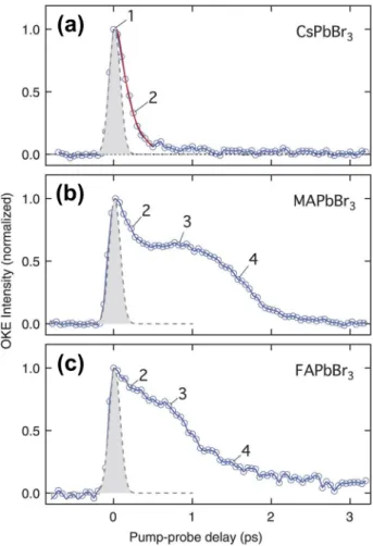
Photoexcitation in MHPs (MAPbBr3, FAPbBr3, and CsPbBr3) with higher energy than their bandgaps at low exciton densities (∼7 ×1016cm−3) does induce the formation of charge carriers at the bandgap edge and also of hot carriers. Anisotropic local reori- entation motion of the organic A-site cations in organic–inorganic hybrid MHPs (e.g., MAPbBr3and FAPbBr3) induces a strong vibra- tional coupling between BX3−andA+, leading to the formation of large polarons. A direct consequence of large polaron formation is the efficient screening of the Coulomb potential. More specifically, it screens the scattering of hot carriers with the longitudinal optical (LO) phonons (i.e., electron–phonon coupling), prevents the ener- getic hot carriers from cooling down, and, thus, forms hot carriers of which∼24% of the PL population is long-lived (∼0.5 ns).56Time- resolved optical Kerr effect (TR-OKE) responses revealed liquid-like dynamics in MAPbBr3and FAPbBr3, but not in CsPbBr3(Fig. 2).
This finding correlates well with the presence of long-lived hot car- riers in the former and suggests the role of organic molecular dipole motion in energetic carrier protection.56Recently, CsPbBr3(or all- inorganic MHPs, in general) was also reported to have polarons due to soft, polarized, and flexiblePbBr6−4 frameworks that can read- ily couple with charge carriers.58–61These large polarons formed by electron–phonon or vibronic coupling between excess charge carri- ers and highly ionized crystalline lattices are widely delocalized in crystals (over several unit cells) and can screen the scattering of hot carriers with LO phonons and, thus, remarkably reduce the cooling rate of hot carriers. In other words, once a large polaron protection shield is formed around an electron or hole, the Coulomb interaction [VLR] responsible for its scattering with LO phonons is screened, leading to a drastically reduced rate of hot-carrier cooling.56Further- more, polarons themselves recombine much more slowly than do charge carriers.58,61Thus, the formation of large polarons can reduce the recombination rate of charge carriers and, thus, limit the LE of MHPs. One effective strategy of suppressing the formation of large polarons, thus increasing the LE, is to physically confine the size of polarons by suitably exploiting nano-sized grains in 3D MHPs, which concomitantly causes a remarkable increase ink1(exc)by the exciton confinement.4,13 The electron-lattice coupling strength of a large polaron (i.e., Fröhlich polaron) is given by the following unitless parameter:
α=e2
̵hc
√ mbc2 2hω̵ LO[ 1
εr(∞)− 1
εr(0)], (9) wherembis the effective mass given by the band structure (i.e., not adjusted for polaronic effects) andωLOis the LO-phonon angular frequency. Forα≤2 which is probably valid for MHPs, the polaron radius (Rp) is inversely proportional to (ωLO)1/2and is given by
R2p≈ 2̵h mbωLO(1−α
6). (10)
For stronger electron–phonon coupling (α≫1), a different form of Rp, which is inversely proportional toα, is used,Rp= (3π/2√
2α).65
FIG. 2. Time-resolved optical Kerr effect (TR-OKE) responses from (a) CsPbBr3, (b) MAPbBr3, and (c) FAPbBr3. The TR-OKE transients of (b) MAPbBr3and (c) FAPbBr3[both belong to hybrid organic-inorganic perovskites (HOIP)] all show characteristic long-time responses covering a broad time window, from∼102fs to∼2 ps. Indeed, both HOIP spectra are similar to typical TR-OKE responses from anisotropic molecular liquids, revealing liquid-like reorientational dynamics in MAPbBr3or FAPbBr3. On the contrary, the signal from CsPbBr3(a) does not show any indication of liquid-like reorientational dynamics but is characterized by (i) an instantaneous electronic response (identical to the pump-probe cross correlation, corresponding to the gray region with 70 fs full width at half-maximum) and (ii) an ultrafast response with a lifetime (τ) of 140±10 fs (red curve). This ultrafast response was attributed to fast reorientation of the local polarization anisotropy.
Reproduced with permission from Zhuet al.Science353, 1409 (2016). Copyright 2016 The American Association for the Advancement of Science.
The parameterαwhich is proportional toVLRis roughly twice the total number of phonons in the phonon cloud (α≈2N) of a given electron or hole, and thus, polaronic effects are likely to be sig- nificant when αbecomes order-unity or larger. αvalues of three common MHPs are 2.17 for MAPbCl3, 1.69 for MAPbBr3, and 1.72 for MAPbI3.24,66 Thus, the electron-lattice coupling in MHPs is considered to be significant.
The large polaron model also explains the inverse dependence of long-lived excess electronic energy on the excitation density.56 Because of the competition for nuclear polarization, there is an effective inter-polaron repulsive interaction that destabilizes large
polarons at high excitation densities. As a result of this destabiliza- tion of the large polaron protection shield (reduced screening effect), the cooling rate of energetic hot carriers by LO-phonon scattering increases with the excitation density up to the onset of a hot-phonon bottleneck (1018cm−3).56Beyond this level, the effective tempera- ture of the more free-electron/hole-like carriers increases again with the excitation density.67
Under high excitation densities (>1018 cm−3), excess hot phonons are generated, so phonon reabsorption can occur.64This process, termed hot-phonon bottleneck, slows down the cooling of hot carriers and, consequently, limits the bimolecular recombination rate (k2) in MHPs. This seems plausible due to the known strong coupling between electrons and the Pb-X (halide) longitudinal opti- cal (LO) phonons68 and low thermal conductivity of MHPs. Hot phonons can reheat the charge carriers and, thus, reduce the cool- ing rate of charge carriers.60Directly after photo-excitation by the photon energy greater than the bandgap of MHPs, the measured transient absorption spectra showed high-energy tails (at∼1.58 eV in MAPbI3) and broadened spectra due to distribution and reabsorp- tion of hot carriers over the bandgap. This is a result of reheating by the phonon bottleneck and increases the lifetime of hot carri- ers.63In MAPbI3, the lifetime of hot carriers gradually increases with the excitation density under the condition of high excitation density (>1018cm−3). This observation confirms that long-lived hot carriers are formed by the hot phonon-bottleneck effect rather than by the polaron effect above the critical excitation density.63
These exciton–ionic lattice interactions can be intensified in low-dimensional (e.g., 2D, 0D) perovskites in which self-assembled quantum wells (in 2D crystals) or nanocrystals (NCs; in colloidal 0D crystals) are bound by a weak van der Waals interaction.37 Many dangling bonds such as out-of-plane self-terminations of PbX6octahedra (in 2D crystals) and NC surfaces (in 0D crystals), and excess charge carriers due to efficient spatial confinement per- turb the lattices and cause strong charge carrier–ionic lattice inter- action.372D MHPs [(C10H7CH2NH3)2PbI4] show a much stronger exciton–LO phonon coupling strength (∼260 meV)37than 3D MHPs (∼40 meV in FAPbI3,∼61 meV in FAPbBr3,∼40 meV in MAPbI3,
∼58 meV in MAPbBr3,68and∼92.1 meV in MAPbI3−xClx25). The strong electron-LO-phonon coupling may reduce the LE but more directly influence the line broadening in PL spectra which, conse- quently, limits the color purity of MHPs. This contribution to the PL broadening [ΔΓLO(T)] can be separately assessed by using the Bose–Einstein distribution function,
ΔΓLO(T) = γLO
[exp(EkBLOT) −1], (11) whereγLO denotes the exciton-LO phonon coupling strength and ELO is an energy representative of the frequency for the weakly dispersive LO phonon branch.68
D. Deep-level defects and ion migration
As discussed in Sec. II B, k2 and k3 are inherent values in MHPs, whereask1is affected by the degree of charge-carrier con- finement and by defect density.37Therefore, recombination path- ways of charge carriers in bulk MHPs are dominantly affected by the defect density. More specifically, the PLQE of MHPs depends
strongly on the defect density because defect-mediated recombina- tion occurs mostly by the SRH-type nonradiative mechanism and is much faster than other radiative recombination pathways [k1(def)
>k1(exc) ork2].69 Therefore, the SRH-type nonradiative recombi- nation via deep-level defects may explain the observed low PLQE in MHPs [Eq.(6)or(7)for fixed k2and k3]. According to first- principles defect-energy calculations,70defects with low formation energies tend to create shallow electronic levels near VBM (accep- tors) or CBM (donors).48In MAPbI3, common shallow-level accep- tors areVPb2−,Ii1−, andVMA1−. On the other hand, common shallow- level donors areMA1+i andVI1+[Fig. 3]. On the contrary, defects hav- ing high formation energies create deep trap levels in the bandgap:
I2−MA,I3−Pbacceptors andPb2+i ,Pb3+I donors (Fig. 3) in MAPbI3.48These deep-level defects act as the SRH-type nonradiative recombination centers. The nonradiative recombination rate [k1(def)] is fast as men- tioned previously. However, the probability of occurrence of deep- level defects is intrinsically low (thus, minority defects) in MHPs owing to their relatively higher formation energies in MAPbI3or CSPbI3.48,71This explains the reported long electron–hole diffusion length and high open-circuit voltage Vocobserved in MHP-based solar cells.72
Although deep-level defects with high formation energies are thermodynamically unfavorable,48,72 they can readily be incorpo- rated into MHP crystals due to their low processing temperatures.
Because MHP crystals are formed at relatively low temperatures (∼25○C for colloidal NCs synthesized by recrystallization meth- ods;73 <100○C for MHP polycrystalline bulk films;4 <200○C for MHP NCs synthesized by hot-injection methods74) and are held together by brittle ionic bonding, they naturally incorporate var- ious types of defects including (i) Schottky defects that are neu- tral vacancy defects (e.g., PbX2 vacancy and MAX vacancy), (ii) Frenkel defects that induce the charge difference in crystals (e.g., elemental defects of Pb2+, I−, and MA+, and unintentional doping), and (iii) structural defects (e.g., lattice distortion by accumulated charges and impurities at grain boundaries). Formation of defect states at surfaces or grain boundaries is accelerated because per- ovskite crystals are susceptible to deformation at the surface (bulk trap density of ∼5 × 1016 cm−3 vs surface trap density of ∼1.6
×1017cm−3for MAPbI3thin films).75These defect states can also be formed by electron–phonon coupling and ion migration.76,77 Schottky-type neutral defects are also readily formed (owing to low defect-formation energies around 50 meV) with their defect-energy levels located between 100 meV and 400 meV below the band edge in MHPs.77Thus, these deep-level neutral defects can trap charge carriers and, consequently, limit the LE of MHPs.
There have been recent reports on PeLEDs regarding over- shooting of luminance at the initial stage of operation.17,78,79 This becomes the major problem of MHPs for their applications to LEDs. However, the underlying mechanism of this phenomenon has not elucidated yet. Because a higher electric field is applied for the operation of PeLEDs as compared to the built-in voltages in perovskite-based solar cells, the ion migration tends to negatively influence the operational stability of PeLEDs. Therefore, it is nec- essary to suppress ion migration in PeLEDs to improve the device lifetime.77,78,80–82This is especially true for the migration on grain boundary (GB). The ion migration is widely known to occur on GB due to its highly unstable nature; thus, blocking the possible migration pathways through the GB can be an effective way to
FIG. 3. The calculated transition energy levels of (a) intrinsic acceptors and (b) intrinsic donors in MAPbI3. Herein, the transition energy level [εα(q/q′)] of a defect is defined as the Fermi-level position where a given defect (namedα) can donate or accept electrons. For the transition between ionic statesqand q′, the two corresponding defect-formation energies should be equal to each other. In other words,ΔHf(α,q) =ΔHf(α,q′).ΔHfcan further be decomposed into three distinct contributions (Ref.
70): (i) the elemental-energy terms (∑iniE(i)) with the defect-energy term [termedΔE(α,q)], (ii) the chemical-potential contributions of constituents (∑niμi), and (iii) the electronic energy (qEF) referenced to the valence band maximum (VBM). Thus,ΔHf(α,q)=ΔE(α,q)+∑niμi+qEF, whereμidenotes the chemical potential of ionic speciesiandEFdesignates the Fermi level. From this relation, one can immediately obtain the following expression of the transition energy level for the defect α:εα(q/q′) =[ΔE(α,q)−ΔE(α,q′)]
(q′−q) .Ab initiocalculations are needed to estimateΔE(α,q), thus,εα(q/q′). Reproduced with permission from Yinet al.Appl. Phys. Lett.104, 063903 (2014). Copyright 2014 The AIP Publishing LLC.
suppress the ion migration and to, consequently, improve the device lifetime.13,83,84
E. Interband transition rates
Yinet al.72have shown that MAPbI3-based perovskites exhibit intrinsic properties that are superior for solar cell applications. These include (i) extremely high optical absorption, (ii) small effective masses for electrons and holes, and (iii) dominant point defects that only generate shallow levels, as discussed in Sec.II D. Accord- ing to Fermi’s golden rule, the strong optical absorption is inti- mately related to the strong optical emission. If the transition moment integral is assumed to be independent ofk(electron’s wave- vector), the photon-emission rate from the conduction band can be written as85,86
Rcv=2π
h̵ ∣∫ ψ∗vHψ˜ cd3r∣2⋅ ∫ 2
8π3δ{Ec(k) −Ev(k) − ̵hω}d3k
=2π h̵
e2 m2o
⎧⎪⎪⎨⎪⎪
⎩
h̵(nph+ 1) 2ωε
⎫⎪⎪⎬⎪⎪
⎭∣∫ ψ∗v(a⋅p)e−kph⋅rψcd3r∣2
× ∫ 2
8π3δ{Ec(k) −Ev(k) − ̵hω}d3k, (12) wherenph is the photon density in the initial state,ψcdesignates the wavefunction in the (initial) conduction state, adenotes the polarization unit vector which is parallel to the electric-field compo- nent of the electromagnetic (photon) wave, and the second integral involving the delta-function denotes the joint density of sate (JDOS) which represents the density of optical transitions that satisfy the Planck condition. According toab initiocalculations,72the JDOS of MAPbI3 is remarkably higher than those of prototypic GaAs and CsSnI3photovoltaics for the photon energy between 2 eV and
3.8 eV, which explains the observed strong optical absorption of MAPbI3-based perovskites in the visible energy range (1.7–3.2 eV).72 Two additional possibilities of enhancing the optical transi- tion rate, thus, PL efficiency, can be deduced by considering the transition moment integral, i.e., the first integral, in Eq.(12),85
∣⟨a⋅pif⟩∣ ≡ ∣∫ ψ∗v(a⋅p)e−kph⋅rψcd3r∣ ≡ ∣∫ ψ∗vP˜aψce−kph⋅rd3r∣
≈ ∣∫ψ∗vP˜aψcd3r∣ ≡ ⟨v|˜Pa|c⟩ =mo
d
dt⟨v|r|c⟩, (13) where ˜Padenotes the electron’s momentum operator component projected on the polarization direction, (=a⋅p). In other words, it represents the interaction of the electron momentum with the vector-field (A) component of the electromagnetic field. Thus, ˜Pa
is parallel to the electric-field component of the emitting electro- magnetic wave (i.e., cosθbetweenaandpwithθ= 0○). The fourth expression was obtained by adopting the so-called dipole approx- imation, namely,e−kph⋅r = 1. This is fairly accurate as the wave- length of the emitting photon (λph) is much longer than the scale of the electron cloud associated with the emission (or absorption), kph⋅r = λ2πphr≈0, sincer≪λphwithλph= order of a few hundred nanometers (∼500 nm) andr= order of 0.1 nm.
According to the Schrödinger picture, the time-dependence of the initial (conduction) and final (valence) stationary states can be written as ∣c(t)⟩ = ∣c(0)⟩eiEct/̵h and ∣v(t)⟩ = ∣v(0)⟩eiEvt/̵h. Using these expressions, the time-dependence of Eq. (13) can be eliminated.85 Thus, the transition moment integral can be rewritten as
∣⟨a⋅pif⟩∣ =mod
dt⟨v|r|c⟩ = imo(Ec−Ev)
̵h ⟨v|r|c⟩ =imoωcv⟨v|r|c⟩, (14)
whereEc−Ev=hω̵ cv. The first point to be considered in Eq.(14) is the odd-even symmetry of the transition moment integral which is directly related to the symmetry of wavefunctions involved in a given optical transition.87In the case of MAPbI3,ψvis represented by the symmetric 6sorbital (+ sign) of Pb2+coupled with the I 5p∗ orbital, whereas ψc is described by the anti-symmetric 6porbital (− sign) of Pb2+ coupled with the I 5p∗ orbital.48,88 The integral
⟨v|r|c⟩in the last expression of Eq.(14)is an even function ofrsince the overall symmetry is⟨v|r|c⟩=⟨+|−|−⟩= +, where “−symmetry ”, for example, denotes an odd function ofr. Thus, the matrix element,
⟨v|r|c⟩, does contribute to a non-zero transition rate. Moreover, this c-vemission in the tetragonal and orthorhombic phases corresponds to a direct bandgap transition at theΓ-point.88,89The second point of emphasis is the transition rate [Rcvin Eq.(12)], i.e., the transition probability per unit time, is proportional to the square of the transi- tion dipole moment, |⟨v|r|c⟩|2. Thus, the PL efficiency of an emitting system which is composed of randomly oriented nanocrystals can be improved greatly if all of the transition dipole moments are aligned along a certain desired direction by employing a suitable experimen- tal technique. Otherwise, a nanocrystalline system having randomly oriented transition dipole moments has a very limited light outcou- pling efficiency since ˜Pa is widely scattered in randomly oriented nanocrystals.
III. STRATEGIES FOR IMPROVING LUMINESCENCE EFFICIENCY
The intrinsic properties of MHPs such as long electron−hole diffusion length and small exciton binding energy at room tem- perature are well suited for their applications to solar cells but are not favorable for LED applications. This is because LED applica- tions, in principle, require a high radiative recombination rate with a low defect density, effective exciton confinement, low optical loss, and charge balance in PeLEDs. To satisfy these requirements in 3D MHP films, optical properties and charge balance should be suit- ably modified during the deposition of MHP films and the fabri- cation of devices. In this section, we will present several recently reported findings and strategies for improving the LE of MHPs and PeLEDs. These strategies are based on the luminescence-limiting factors described previously and include (i) nanometer-scale con- trol of particle dimension, (ii) dimensionality control to 2D and quasi-2D perovskites, (iii) ligand engineering of colloidal NCs and QDs, (iv) control of optical properties and charge balance, and (v) chemical modifications.
A. Nanometer-scale control of particle dimension As discussed in Sec.II A, decreasing the physical dimension from micrometer scale to nanometer scale4,13and decreasing the dimensionality from 3D to 2D or 0D27are two most effective ways of increasing the LE of PeLEDs because these can enhance the LE of MHPs by confining the charge carriers and improving the possi- bility of radiative recombination of electron–hole pairs (excitons).
It is now well known that the PL efficiency of perovskite emit- ters can be improved greatly if the exciton binding energy (Eb) can be increased and the exciton diffusion length (LD) is decreased by reducing the grain size.5An ideal approach to achieve highEband lowLDin perovskite emitters is to effectively confine the excitons in
the form of nanometer-scale (<20 nm) colloidal perovskite nanopar- ticles (NPs) rather than in polycrystalline perovskite bulk films with large grain size (0.1–10μm). These perovskite NPs are in totally dif- ferent research subfields from polycrystalline perovskite bulk films.
Perovskite NPs can be divided into two different regimes: (i) 0D per- ovskite quantum dots (QDs) with a dimension less than the exciton Bohr diameter,DB (the quantum-size regime or strong quantum- confinement regime), and (ii) relatively less explored perovskite nanocrystals (NCs) with a dimension greater thanDB(the regime beyond the strong quantum confinement or beyond the quantum- size effect). Perovskite QDs with size less thanDB(<∼10 nm) showed highEband lowLDand, thereby, achieved high PLQE at room tem- perature.1,73,90–93However, these 0D QDs suffer from strong depen- dence of emission wavelength and color purity on the QD size, as do inorganic QDs.94
The energy of confined excitons (Eexc) in a spherical quantum well (i.e., 0D QD) with the radiusRcan be obtained by considering thatEexcis the sum of the following two distinct contributions: (i) the energy of strongly confined individualeandhparticles [E(α→ ∞)]
and (ii) the spatiale-hcorrelation energy (Ecorr), whereαis a measure of the spatiale-hcorrelation in an exciton withα→ ∞for completely no correlation (individual particle confinement),95–97
Eexc=E(α→ ∞)+Ecorr≈h̵2π2
2μR2− C1e2
4πεoεrR+Ecorr(R→0)
=h̵2π2
2μR2− C1e2
4πεoεrR−0.248Eb, (15)
whereμdenotes the reduced mass of the exciton,Ecorr(R→0) sig- nifies the spatiale-hcorrelation energy in the limit ofR→0, and the binding energyEbis defined in Eq.(1). In Eq.(15), the origin of energy (Eexc) is chosen at the bandgap energy of the bulk crys- tal.98The first two terms in the last expression of Eq.(15)denote the kinetic energy of a very strongly confined individual particle (̵h2π2/ 2 μR2) and the corresponding Coulomb energy (−C1e2/4πεoεrR) with the optimizedC1 = 1.786.95,96 The asymptotic ground-state exciton wavefunction with a non-zero degree of the spatial e-h correlation can be written, using the correlation parameterα, as
ψ(re,rh,reh) =Nj0(πre
R )j0(πrh
R )exp(−reh
α )
=Nsin(πre/R) re
sin(πrh/R) rh
exp(−reh
α ), (16) where N is the normalization constant, reh denotes the distance between the electron and hole in a given exciton quasi-particle (=|re
−rh|), andj0(x) designates the zeroth-order spherical Bessel func- tion. Equation(16)shows thatψ(re,rh,reh) becomes a simple prod- uct ofψ(re) andψ(rh) for a strongly confined exciton underα→ ∞. Under a strongly confined condition, thee-hcorrelation in an exci- ton will be collapsed andEcorr→0. In this strongly confined limit (α
→ ∞), the exciton Bohr radius [Eq.(1)] can be correlated with the critical QD radius for the PL blue shift (Rc) using Eq.(15), namely,
(Rc
aB) =
4πεoεr̵h2π2 2C1μe2 4πεoεr̵h2
μe2
= π2
2C1 ≈2.75. (17)
We neglected thee-hcorrelation energy (Ecorr =−0.248Eb) in the derivation of the above critical ratio. If we included theEcorrterm