A 64k-Bit High-Density OTP ROM Array
with 3-Transistor Cell Standard CMOS Gate-Oxide Antifuse
I.INTRODUCTION
Among various memory types, one-time programmable read-only memory (OTP ROM) is one of the cheapest memories in storing data which can be configured permanently after fabrication. There are many types of OTP, most of which are based on either fusing or anti-fusing. Poly or metal fusing method using laser instrument has widely been used in most of the memory manufacturer’s for the memory cell repair for high-density memories, such as DRAM and SRAM. This, however, is not only very expensive, but has a limitation that it can only be done on wafer test, and that it is impossible to use at final test after packaging[1].
Poly fusing using joule heating has also been tried for trimming various CMOS analog circuits, such as, CMOS RF circuits, CMOS OP Amps, and ADC’s and DAC’s requiring on- chip trimming ROM to compensate for the process variations, device mismatches and so on[2]. However, this is not reliable enough to be used for manufacturing.
Antifuse based on anti-fusing thin oxide between two conductors is more reliable and has been adopted successfully in some commercial circuits. The metal-oxide-metal antifuse used in the field programmable gate array (FPGA) from Actel[3] is one of the well-known examples. Many types of FPGA products, which have on-chip programmable ROMs (PROM) based metal-oxide-metal antifuses, are provided for high-performance and low-cost programmable ASIC applications. Antifuse using oxide-nitride-oxide (ONO) capacitor cell in
DRAM proposed for repairing the failed memory cells at package level as well as at wafer level[4]-[5], are notable examples. The ONO antifuse OTP ROM has very reliable antifuse characteristics such as breakdown voltage, low after-breakdown resistance, long-term reliability and so on. But the metal-to-metal antifuse structure from Actel and the ONO antifuse from Hynix are not directly applicable to standard CMOS products because metal- thin insulator-metal structure and ONO capacitor is not available for standard CMOS process technology.
One of the most promising candidate as an antifuse element with standard CMOS technology is the gate oxide. Until recently, gate oxide breakdown voltage is much higher than that of the power supply. However, due to the continued scaling of gate oxide which is much faster than the power supply voltage scaling, we are now in a position to consider antifuse based on very thin gate oxide[6]. In addition to antifuse element, for OTP ROM to be useful, high voltage switching circuitry is also needed to program OTP ROM selectively. In general, high voltage CMOS device is needed for this, which requires process change. The drift nMOS technology with antifuse based on gate oxide breakdown is a good example, but it needs large chip area and additional masks[7]. The construction of this high voltage circuitry using low voltage standard CMOS devices is a great challenge.
In this paper, we propose a novel 3-transistor OTP ROM cell, which is fully compatible with the standard CMOS process technology. It is based on 1-transistor for antifuse and 2 additional transistors as high voltage blocking and cell access devices. Ch. II describes nMOS antifuse characteristics. The operation of OTP ROM array employing proposed 3-T cell is explained in detail in Ch. III and 64-kb high-density OTP ROM is shown in Ch. IV followed by conclusions.
II.CMOSANTIFUSE 1. Antifuse element
Antifuse and fuse are well-known devices for their special electrical properties. Their states are to be changed in case that high voltage or high current is applied to their both electrodes during programming, and then, their states are preserved. In case of antifuse, the state changes from capacitor to resistor by high-voltage or high-current programming. The antifuse element has capacitive characteristic with very large pre-breakdown resistance of ROFF ( >1GΩ in nMOS antifuse). During the programming mode, the medium insulator layer is permanently broken down for applied programming high-voltage or high-current. And then, the medium material is no more insulator but it is a conductor with small post-breakdown resistance of RON ( <50kΩ in nMOS antifuse).
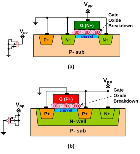
Single nMOS (or pMOS) device is used for an antifuse element which is composed of two electrodes, that is, gate-poly electrode and a tied Source/Drain node electrode, and medium insulator material of gate oxide. Fig.1 (a) shows the schematic for nMOS antifuse programming mode, where the programming high voltage of VPP whose value is much higher than the power supply voltage (VPP > 3VDD) applied to the nMOS gate. The channel is inverted and the source/drain edge region below the gate is accumulated, in which the high electric field is applied in edge region. But the area of source and drain edge (gate-to- source/drain overlapped region) is extremely small and the potential difference between source/drain edge and channel region is not large enough because the channel is inverted, the breakdown occurs in the channel region as well as the source/drain overlapped region. The location for this breakdown is schematically shown in Fig. 1 (dotted circles). We have found that the similar phenomena happen in the pMOS antifuse, which in shown in Fig. 1 (b).
VPP
P- sub G (N+)
VPP
channel N+
P+ N+
BD BD BD
Gate Oxide Breakdown
(a)
P- sub N- well
N+
G (P+) channel
P+ P+
BD BD BD
VPP
Gate Oxide Breakdown
VPP
(b)
Fig. 1. CMOS antifuse structures during the programming mode ; (a) circuit schematic and cross sectional view of nMOS antifuse showing the ruptured regions (shown as dotted circles) for channel breakdown (VPP>0), and (b) those of nMOS antifuse.
2. CMOS antifuse breakdown characteristics : time-to-breakdown
The time-to-breakdown in intrinsic oxide films is known as the empirical quantitative model[8] which is based on the theoretical basis of the statistical reliability model for intrinsic failures. And the equation is verified with experimental methods. Two different types of antifuse samples which are implemented with two different process technologies; TSMC 0.18µm and ANAM 0.25 µm CMOS process. Each of 100 samples is measured for statistical analysis, which is shown in the Fig. 2. The measurements are performed with nMOS antifuse
samples, blocking resistor of RBLK which can limit maximum current flowing through the antifuse and semiconductor parameter analyzer.
The statistical distribution of time-to-breakdown is explained for the Weibull distribution[9]. From this distribution, we can estimate the average programming time (1-bit programming time) for a multi-bit OTP ROM array. In the TSMC 0.18µm antifuse, the average value (µ) of 6.37ms and the standard deviation (σ) of 4.47ms are approximated to the Weibull distribution, and then, if the programming duration is above 70 milli-seconds, at most 1-bit failure occurs for every over 1 tera-bits (1012 bits) programming. Similar prediction can be applied to the ANAM 0.25µm antifuse measured data, we can find the time-to-breakdown value of above 800 ms for the same 1-bit failure rate.
0 20 40 60 80 100
0 50 100 150 200 250 300
time-to-breakdown [m sec]
Cumulativ e dis tr ibution [%]
TSMC 0.18µm
T
OX= 40Å, V
PP= 6.5V, R
BLK= 1.5kΩ
ANAM 0.25µm
T
OX= 58Å, V
PP= 9.5V, R
BLK= 3.0kΩ
Fig. 2 Measured time-to-breakdown distributions with two different processes for each 100 nMOS samples; TSMA 0.18µm (mean(µ) = 6.37ms, standard
deviation(σ) = 4.47ms ) and ANAM 0.25µm (mean(µ) = 128ms, standard deviation(σ) = 68.8ms ) CMOS process
3. CMOS antifuse breakdown characteristics : post-breakdown resistance (RON)
The post-breakdown resistance of RON is a very important characteristic for antifuse OTP ROM because the programmed characteristics of antifuse OTP ROM, such as reading speed or access time, are mainly dependent on the RON. The difference of RON is fairly influenced by the material of two electrodes of antifuse, the supplied current during antifuse rupture, and the area of the breakdown spot which is made from thermal reaction because of high-current flowing through the ruptured antifuse[10]-[11].
0 20 40 60 80 100
0 2 4 6 8 10
Post-breakdown resistance : R
ON[k Ω ]
Cu m u lative dist ribution [%]
TSMC 0.18µm, TOX= 40Å CC=1mA, VDD= 2.0V
ANAM 0.25µm, TOX= 58Å, CC=1mA, VDD= 2.5V
Fig. 3 Measured post-breakdown resistance (RON) distributions with two different processes for each 100 nMOS samples; TSMC 0.18µm (mean(µ) = 2.24kΩ, standard deviation(σ) = 1.60 kΩ) and ANAM 0.25µm (mean(µ) = 0.544kΩ,
standard deviation(σ) = 0.193kΩ) CMOS process after the same breakdown conditions of time-to-breakdown measurements.
The RON distributions for two types of antifuse samples (TSMC 0.18µm and ANAM 0.25µm process) are shown in Fig. 3. The RON values are measured at the sweep mode of which the measuring instrument is the semiconductor parameter analyzer after antifuse breakdown. The breakdown conditions of two types of antifuse samples are the same as those of time-to-breakdown measurements which are the applied high-voltages of VPP (VPP_TSMC = 6.5V and VPP_ANAM = 9.5V), the programming times of tPGM (tPGM_TSMC = 100ms and tPGM_ANAM = 1s), and the current compliances (CC) of 1mA for both cases.
0 10 20 30 40 50
0 20 40 60 80 100
CC = 1mA CC = 0.3mA CC = 0.1mA
Cum u la ti v e di st ri but ion [ % ]
R
ON[k Ω ] at V
DD
= 1.5V
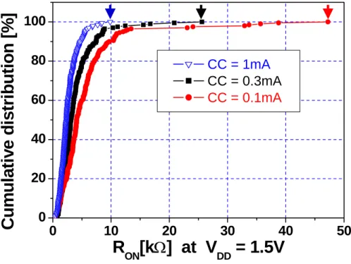
Fig. 4. Measured cumulative distributions of RON for each 200 nMOS antifuse samples with three different current compliance (CC) conditions of 1mA, 0.3mA, and 0.1mA; parameters of averages (µ) and standard deviations
(σ) are µCC=1mA = 2.70kΩ, σCC=1mA = 1.57kΩ, µCC=0.3mA = 3.97kΩ, σCC=1mA = 3.14kΩ, µCC=0.1mA = 5.68kΩ and σCC=0.1mA = 6.19kΩ. The 1.2µm/0.18µm sized nMOS antifuse samples with ANAM 0.18µm process are used.
One of the important elements to determine the RON is the supplied current during the antifuse rupture[12]-[13]. To verify the correlation between supplied current and post- breakdown resistance, I have measured 600 antifuse samples with different current compliance conditions of 1mA, 0.3mA, and 0.1mA. The measured plot and statistical parameters of averages and standard deviations are shown in Fig. 4. The measured results show that average values of RON and standard deviations are increased as the current compliances are decreased, and more over, the increase of standard deviation is faster than that of the average value, which tell us that we must determine the value of RON in the worst condition not to malfunction in the OTP ROM array.
III.3-TRANSISTOR CMOSANTIFUSE OTPROMARRAY
To use CMOS antifuse as a storage element for an OTP ROM array, we propose 3-T OTP ROM cell as shown in Fig. 5(a), which is composed of an nMOS antifuse, a high-voltage blocking nMOS, and a cell access transistor. In the program mode, externally supplied high- voltage of VPP is applied to tied gates of all nMOS antifuses though single external pin, and only one of antifuse cell selected by corresponding word-line and bit-line signals, is ruptured.
In the read mode, VDD is applied to the VPP node, instead. This alleviates the use of high- voltage switching, making it compatible with standard CMOS technology. The reading current flows through the antifuse to bit-line at the programmed cell, which is detected by the bit-line sense amplifier, while very small tunneling current (<100pA) flows through the non-
programmed antifuse cell.
Antifuse
HV blocking
Cell Access
VG-BM
BL WL
VPP
(a)
WL0
WL1
BL0 BL1
‘Word-Lime (WL)’
•Selected : VDD •Non-selected : GND‘Bit-Line (BL)’
• Selected : GND
• Non-selected : VDD
… … …
V
PPH
L
…
…
V
G-BM(=V
DD)
L H
Selected cell
(b)
Fig. 5. 3-transistor OTP ROM cell array; (a) a 3-T cell which is composed of an nMOS antifuse, a high voltage blocking nMOS and a cell access transistor, and (b) programming mode OTP ROM array which is composed of several unit (3-T) cells.
Using the previous antifuse measurement results of TSMC 0.18µm process, we have designed, fabricated and measured the 4-bit OTP ROM array. The design parameters of antifuse have been determined by statistical considerations, that is, the target RON and time-to- breakdown are 50kΩ and 100ms for unit cell, respectively. These target values are quite large
enough not to malfunction during above several tera-bits programming and reading because the standard deviations of target RON and time-to-breakdown are 30σ and 21σ, respectively.
WL0
WL1
BL0 BL1
… … …
VPP
H
L
…
…
VG-BM (=VDD)
L H
Selected cell
…H
BL2 WL2L
… Non-selected cell
Non-selected & already broken antifuse cell Non-selected
Unbroken antifuse cell
Broken Antifuse
(0,0) (0,1) (0,2)
(1,0) (1,1) (1,2)
(2,0) (2,1) (2,2)
Fig. 6 Operations of 3-T CMOS OTP cell array during programming ; selected cell for programming (cell 0,0), non-selected cells with unbroken antifuse (cells (0,1), (1,1), (1,2) and (2,0)), and non-selected cells with already broken antifuse (cells (0,2), (1,0), (2,1) and (2,2))
From now on, I’d like to show you several states of 3-T antifuse ROM cell during the programming mode such as a selected cell, a non-selected and already broken antifuse cell and a non-selected and unbroken antifuse cell, and some possible problems and their solutions, which is schematically shown in Fig. 6.
1. Selected cell
In the selected cell of cell(0,0) shown in Fig. 6, after antifuse breakdown, the programming high voltage would directly be applied between the drain of blocking nMOS and P-substrate in case of small RON. From this high-voltage, the parasitic bipolar junction transistor(BJT), which is composed of drain(N)-body(P)-source(N) of blocking nMOS, is turned on, as the RON is decreased. Small RON with constant current supply reduces the voltage difference between the two electrode of antifuse, the drain-to-body current from the parasitic BJT increases as the drain voltage of blocking nMOS raised and then, more current flows through the antifuse and the blocking nMOS.
To avoid this situation, we inserted a blocking resistor of RBLK between the high- voltage supply node and the drain nodes of blocking nMOS’s, which also helps to keep constant current supply for uniform rupturing of antifuse. The value of RBLK is determined by the drain voltage of blocking nMOS (VDRAIN), by the RON of antifuse and by the current flow through the blocking nMOS. If the RON or the supplied current flow is sufficiently large, no RBLK is needed because the VDRAIN is low enough not to turn on the parasitic BJT of the blocking nMOS. In real circuit designing step, we cannot determine the RON as a constant value but the smallest RON value is considered as a worst condition (in this case only, generally, smaller RON is a desirable condition) of RON. From the previous Ch. 2, the minimum RON is assumed to be 500Ω at the supplied current of 1.5mA. And then we can plot the load-line for the selected cell of the 3-T OTP ROM shown in Fig. 7. To add the RBLK, the
operation point is moved to the left (lower operation voltage), and we can predict and control the proper circuit operation.
RBLK
Increased Minimum RON(0.5kΩ) + RBLK(1.5kΩ) RBLK = 2.0kΩ
RBLK = 3.0kΩ
Operating point : VOP
0 1 2 3 4
0 1m 2m 3m
C e ll c u rre n t : I
CELL[A ]
S/D node voltage of AF : V
AF-S/D[V]
Fig. 7 Load-line plot for the selected cell with various blocking resistance of RBLK; as RBLK is increased the operating voltage of VOP is decreased ( RBLK of 1.5kΩ, 2.0kΩ and 3.0kΩ, when the minimum RON is 0.5 kΩ).
2. Non-selected and unbroken antifuse cell
As for the case of non-selected cell with unbroken antifuse shown in Fig. 6 where the cells are (0,1), (1,1), (1,2) and (2,0), we also find that there are no disturbance problems because the high-voltage is not applied to the antifuse. The tied drain/source node voltage of antifuse is so high that the gate oxide of antifuse is not ruptured during programming. And the operating point is settled at which a supplied current from the antifuse (Fowler-Nordheim tunneling current) is equal to the summation of leakage currents in which the dominant leakage current is the gate induces drain leakage(GIDL) current of blocking nMOS.
0 2 4 6 8 10 1f
100f 10p 1n 100n
Cel l cur rent : I
CELL[A ]
Applied high voltage : V
PP[V]
HV = 6.5V (VPP)
WL=H, BL=H WL=L, BL=H GIDL of
cell access GIDL of Blocking nMOS
WL=L, BL=L
0 2 4 6 8 10
1f 100f 10p 1n 100n
Cel l cur rent : I
CELL[A ]
Applied high voltage : V
PP[V]
HV = 6.5V (VPP)
WL=H, BL=H WL=L, BL=H GIDL of
cell access GIDL of Blocking nMOS
WL=L, BL=L
Fig. 8 Non-selected and unbroken antifuse cell; two types of measured plots show that only below 10pA currents flow when the high voltage of VPP is applied 6.5V. And the breakdown voltage is at least 10V, which is very large voltage margin to be compared with process technology of the TSMC 0.18µm.
The measured data plot is shown in Fig. 8. The applied high voltage of VPP is swept from 0V to 10V in 50mV steps and the cell current of ICELL is measured at that node with semiconductor parameter analyzer. And the measured 3-T OTP ROM samples are fabricated with TSMC 0.18µm CMOS process. Two different plots show the different non-selected and unbroken antifuse cell conditions, which is determined from different input signals of word- line and bit-line. And the breakdown voltage of non-selected and unbroken antifuse cell is more than above 10V, which is very large voltage margin to be compared with this process technology.
3. Non-selected and already broken antifuse cell
In the non-selected and already broken antifuse cells which are shown in Fig. 6 where the cells are (0,2), (1,0), (2,1) and (2,2), the programming high-voltage is directly applied to the drain node of blocking nMOS because the blocking resistor (RBLK) and the broken antifuse resistor (RON) are negligibly small to be compared with off-state resistance of blocking nMOS. But the high voltage applied to the drain of blocking nMOS can rupture the gate oxide of blocking nMOS. Fortunately, the gate voltage of blocking nMOS is common VDD of 2V, and therefore no high voltage is applied between the gate-to-drain of blocking.
Moreover, the area of which a drain is overlapped with a gate is very small, the breakdown voltage of blocking nMOS is very high enough not to be ruptured.
0 1000 2000 3000
0 1µ 2µ 3µ 4µ 5µ 6µ
High voltage = 6.5V High voltage = 6.7V High voltage = 6.9V
C e ll c u rre n t : I
CELL[A ]
Elapsed time [sec]
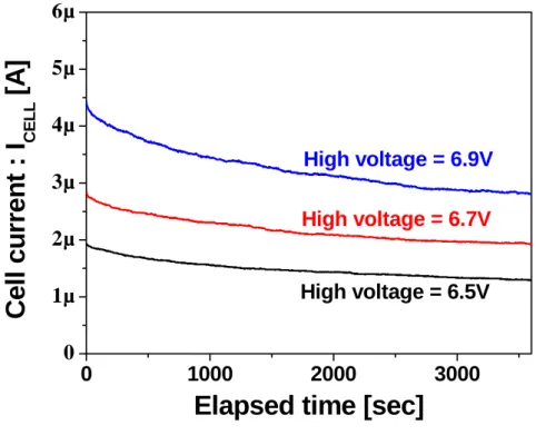
Figure 4.7 The GIDL current vs. elapsed time with three different programming high voltages of 6.5V, 6.7V and 6.9V are applied during long
programming time of one hour in the non-selected and already broken antifuse cell corresponding to Fig. 6 where the cells are (0,2), (1,0), (2,1) and (2,2).
Fig. 9 shows the GIDL current vs. elapsed time for different programming high- voltages of 6.5V, 6.7V and 6.9V during long programming time of one hour. When the programming high-voltage of above 6.5V is applied, for long programming time, the blocking nMOS is not only ruptured but also damaged by supplied high voltage.
0 1 2 3 4 5 6
1f 1p 1n 1µ 1m
C e ll c u rre n t : I
CELL[A ]
S/D node voltage of antifuse : V
AF-S/D[V]
GIDL of blocking nMOS Non-selected & broken AF AF Breakdown
Selected cell
Non-selected
& unbroken AF
(a) (b)
(c)
0 1 2 3 4 5 6
1f 1p 1n 1µ 1m
C e ll c u rre n t : I
CELL[A ]
S/D node voltage of antifuse : V
AF-S/D[V]
GIDL of blocking nMOS Non-selected & broken AF AF Breakdown
Selected cell
Non-selected
& unbroken AF
(a) (b)
(c)
Fig. 10 Load-line analysis for three states of OTP ROM cell during the programming mode ; (a), (b), and (c) the load-line plots – the cell current of ICELL vs. S/D node voltage of antifuse (VAF-S/D)
4. The load-line analysis for 3-T OTP ROM cell during the programming mode Fig. 10 shows the load-line plot for three states of OTP ROM cells, which is from the
measurement of the cell current as the source/drain node voltage of an antifuse (drain node voltage of blocking nMOS) is varied. Two main currents, shown in the load-line plot, are the tunneling current of antifuse and the GIDL current of blocking nMOS.
As the S/D node voltage of antifuse (VAF-S/D) is decreased, the tunneling current through the antifuse is increased and at some critical point of VAF-S/D, the gate-oxide of antifuse is broken-down(Fig. 10(a)). On the other hand, in the non-selected and already broken antifuse cell, the GIDL current of blocking nMOS is increased as the VAF-S/D is increased (Fig. 10(b)). From these two groups of plots, we can find the operation points of non-selected and unbroken antifuse cells, which are the cross-points of these two groups of plots (Fig. 10 (c)). The operating point (VAF-S/D) of non-selected and unbroken antifuse cell is about 3.5V, and the cell current flows merely 10pA and this result is fairly well matched with the Fig. 8 in Sec. III-2.
5. 3-T OTP ROM array measurements
4-bit OTP ROM array, which is fabricated with TSMC 0.18µm, is measured with programming high-voltage (VPP) of 6.5V, normal operation voltage (VDD) of 2.0V, and programming duty of 100 ms. Measurements are performed with two steps. In the first step, two-bit (cell 1,0 and cell 1,1) cells are successively programmed with input ‘HIGH’ signals of (WL1, BLS0) and (WL1, BLS1) during the programming mode. Second, in the reading mode, two bit cells of cell 0,0 and cell 1,0 are read using input ‘HIGH’ signals of (WL0, BLS0) and (WL1, BLS0) for reading the non-programmed (cell 0,0) and programmed (cell 1,0) cells, which is shown in Fig. 11(a), and the chip microphotograph is shown in Fig. 11(b). The cell area occupies 20µm2 for 1-bit cell, in case of TSMC 0.18µm process.
The programming cell measurement waveforms are shown in Fig. 12. When WL1 and BLS1 are ‘HIGH’ where the programming high-voltage is commonly applied to the VPP
node, the cell 1,1 is selected for programming. To measure the breakdown moment we have measured the gate voltage of antifuse (VAF-G), which is shown in Fig.11(a) and Fig. 12(a). The antifuse breakdown happens after address signals input with WL and BLS, and some time duration of time-to-breakdown, the nMOS antifuse of selected cell is ruptured, which is shown Fig.12 (a). The antifuse gate voltage of VAF-G is lowered to about 4.7V and the cell current of ICELL is about 1.3mA, in case of 4-bit OTP ROM with TSMC 0.18µm process.
cell 1,1 cell 1,0
VAF-G WL0
WL1
BL0 BL1
VDD RBLK
BL-SA1 Dout0
BLS0 PGM
VBIAS
Dout1
BL-SA0
BLS1
cell 0,0 cell 0,1
PGM
READ
BL-SA 2-b cell 2-b
cell 4-bit OTP ROM array
6µm 7µm 14µm
BL-SA 2-b cell 2-b
cell 4-bit OTP ROM array
6µm 7µm 14µm
(a) (b)
Fig. 11 (a) Cell schematic and (b) microphotograph for 4-bit OTP ROM array measurements; the OTP ROM is composed of 4 cells, 2 BL-SAs, 2 BLs and 2 WLs, which is fabricated with TSMC 0.18µm process.
BLS1 WL1 VAF-G BLS0
BD
PGM cell 1,0 Cell current
: ICELL[A]
0.5m 1.0m 1.5m
0
PGM cell 1,1
4.7V BD 6.5V
100m sec
BLS1 WL1 VAF-G BLS0
BD
PGM cell 1,0 Cell current
: ICELL[A]
0.5m 1.0m 1.5m
0
PGM cell 1,1
4.7V BD 6.5V
100m sec
(a)
OUTPUT
Broken AF cell Unbroken AF cell
READ cell 1,0 READ cell 0,0
BLS0 WL1 WL0
15µsec
OUTPUT
Broken AF cell Unbroken AF cell
READ cell 1,0 READ cell 0,0
BLS0 WL1 WL0
15µsec
(b)
Fig. 12 4-bit OTP ROM array measured data with TSMC 0.18µm process;
(a) programming mode cell current at the high-voltage supply node (which is measured with semiconductor parameter analyzer), and input/output signal waveforms (which are measured with oscilloscope), and (b) reading mode measurement results (which are measured with oscilloscope)
IV.64-KB HIGH-DENSITY OTPROM
To implement high-density OTP ROM array, we have considered two important issues such as smaller area consumption and more reliable operation during long programming time. The CMOS antifuse OTP ROM uses a high-voltage node to program the storage cell, and the programming time, which is the time-to-breakdown of MOSFET device, is greatly dependant on the programming high-voltage. Therefore the reliable structure for high-voltage and long programming duration is necessary.
BLOCK 0 × 0
WL1
WL0
BL1 … BL0 …
VPP
…
…
RBLK0
BL Dout1 -SA0
BLS1 PGM
VBIAS
Dout0
BLS0
R1 R2 VG-BM
PGM
Global VG-BM generation circuit
(a)
BL -SA1
BLOCK n × 0
BLOCK 0 × m BLOCK
n × m
… …
…
…
…
…
…
… …
…
…
…
…
…
BLn
WLm RBLKm
RBLKn×m
RBLKn
(b)
Fig. 13 The high-density OTP ROM structure; (a) the high-voltage blocking nMOS biasing circuit using programming high-voltage, and (b) the high-density
OTP ROM structure which is composed of a group of blocks and a global blocking nMOS biasing circuit.
We propose a block structure for the GIDL current of blocking nMOS in the non- selected and already broken antifuse cell during the programming mode. The GIDL current is at most a few µA in a unit cell, but in several thousands of OTP ROM array the GIDL current is more than several mA. This GIDL current and a blocking resistor (RBLK) make programming voltage drop between two electrodes of antifuse. A unit block, which is composed of several hundreds of cells and a blocking resistor, which is shown in Fig. 13(b), can solve this problem.
In the non-selected and already broken antifuse cell, another possible problem is the gate-oxide reliability of blocking nMOS, which can be broken-down during very long programming time. The voltage difference between drain and gate of blocking nMOS is VPP - VDD, and this is very large to be compared with normal operation voltage of VDD
(in the TSMC 0.18µm process, it is 4.5V). To avoid this situation, we introduce the high- voltage gate biasing of blocking nMOS. In Fig.13 (a), we show the global VG-BM biasing circuit, which is made of just two resistors and one nMOS.
From these considerations, we have designed the 64-kb high-density OTP ROM array, which is shown in Fig.14, is fabricated with ANAM 0.18µm CMOS process and measured with logic analysis system with pattern generator. The 64-kb OTP ROM array is composed of address decoders and input/output part including current sense amplifiers. Eight of 8-kb cells with 128 unit blocks consist the whole 64-kb cell array, and the unit block is composed of 64- bit 3-T cells and a blocking resistor of RBLK. These cells are accessed by 256 of word lines and bit lines, respectively, decoded from 16-bit address signals which are inputted from
external pins.
Unit Block
B0 B1 B2 B3 B4 B5 B6 B7
Row (Y) DEC
CSA&
Latch 0
Column (X) DEC
Output Buffer 32-bit 256-bit
256-bit
WL8
8 BL
CSA&
Latch 1
CSA&
Latch 14
CSA&
Latch 15 CSA&
Latch 2
CSA&
Latch
3
…
2-bit
DOUT 1
32-bit
2 CTRL
(a)
(b)
Fig.14 64-kb OTP ROM array ; (a) OTP ROM structure, and (b) the implemented chip microphotography with ANAM 0.18µm process
Fig. 15 shows the Shmoo plot of the 64-kb OTP ROM measurement during the reading mode after known data programming. In the normal operation voltage of 2V(=VDD)
the reading operation is properly performed within 500ns. The 64kb OTP ROM consumes about 1300µm×600µm for storage 3-T OTP cells, decoders, current sense amplifier and input/output buffers.
1.2 1.5 2.0 2.5
1 2 3 4 5 6 7 8
0 9 10
Pass
Fail
Reading delay : t
READ[µsec]
Su pply voltage : V
DD[V]
Fig. 15 The 64-kb OTP ROM array measurement result – Shmoo plot during reading mode operation.
V.CONCLUSIONS
The CMOS antifuse has very large pre-breakdown resistance of ROFF ( >1GΩ ) and small post-breakdown resistance of RON ( <100kΩ ), and therefore, large design margin, which is the ratio of the two resistance values, of more than four orders of magnitude can be acquired. The current limited condition, during the antifuse breakdown, has an influence on the RON characteristic. As the supply current is increased, the RON is decreased, which is shown in several measured plots with statistical analysis. These results show that the CMOS antifuse has expectable and reliable characteristics for CMOS antifuse OTP ROM.
Using the CMOS antifuse, we have proposed the 3-transistor cell OTP ROM array which is implemented with standard CMOS process, and proved its correct operation. The 3-T cell antifuse OTP ROM is composed of an nMOS antifuse, a high-voltage blocking nMOS, and a cell access transistor. In the programming mode, single externally supplied high-voltage is applied to tied gates of nMOS antifuses, and the high-voltage is replaced by the VDD during the reading mode. The operation of 3-T antifuse cell has been analyzed into several different cell states in the programming mode, such as the selected cell, the non-selected with already broken antifuse cell, and non-selected and unbroken antifuse cell. From this reliable operation, we have proposed high-density antifuse OPT ROM structure, which has a block structure and a high-voltage gate biasing circuit of the blocking nMOS. And then, the 64-kb antifuse OTP ROM has been designed, fabricated with ANAM 0.18µm standard CMOS process, and confirmed of its correct operation with measurement.
References
[1] Chih-Yuan Lu, James D. Chlipala, and Leonard M. Scarfone, “Explosion of Poly-Silicide Links in Laser Programmable Redundancy for VLSI Memory Repair”, in IEEE Transaction on Electron Devices, vol.36, No.6, pp.1056-1062, Jun., 1989
[2] O.Kim, C.J.Oh and K.S.Kim, “CMOS trimming circuit based on polysilicon fusing”, in Electronics Letters, vol.34, No.4, pp.355-356, Feb., 1998
[3] http://www.actel.com/documents/antifusePIB.pdf
[4] Jae-Kyung Wee, Jeong-Hoon Kook, Sang-Hoon Hong, and Jin-Hong Ahn, “Antifuse Circuits and Their Applications to Post-Package of DRAMs”, in Journal of Semiconductor Technology and Science (JSTS), vol.1, No.4, pp.216-231, Dec., 2001
[5] Joo-Sun Choi, Jae-Kyung Wee, Ho-Youb Choi, Phil-Jung Kim, Jin-Keun Oh, Chang-Hyuk Lee, Jin-Yong Chung, Sea-Chung Kim, and Woodward yang, “Antifuse EPROM Circuit for Field Programmable DRAM”, in IEEE International Solid-State Circuit Conference (ISSCC) 2000, pp.406-407
[6] Jinbong Kim, and Kwyro Lee, “3-Transistor Antifuse OTP ROM Array Using Standard CMOS Process,” in Symposium on VLSI circuits 2003, pp. 223 – 226. June 2003
[7] Philippe Candelier, Nathalie Villani, Jean-Pierre Schoellkopf, and Patrick Mortini, “One Time Programmable Drift Antifuse Cell Reliability”, in IEEE International Reliability Physics Symposium, pp.169-173, 2000
[8] J. C. Lee, I. –C. Chen, and C. Hu, “Modeling and Characterization of Gate Oxide reliability,” in IEEE Transactions on Electron Devices, vol.35, No.12, December 1988, pp.2268-2278
[9] R. Degraeve, J. L. Ogier, R. Bellens, P. J. Roussel, G. Groeseneken, and H. E. Maes, “A
New Model for the Field Dependence of the Intrinsic and Extrinsic Time-Dependent Dielectric Breakdown,” in IEEE Transitions on Electron Devices, vol.45,pp.472-481, 1998 [10] Guobiao Zhang, Chenming Hu, Peter Y. Yu, Steve Chiang, Shafy Eltoukhy, and Esmat Z.
Hamdy, “An Electro-Thermal Model for Metal-Oxide-Metal Antifuses,” in IEEE Transitions on Electron Devices, vol.42, pp.1548-1558, 1995
[11] Marc Porti, Marie-Christine Blüm, Montserrat Nafría, and Xavier Aymerich, “Imaging Breakdown Spots in SiO2 Films and MOS Devices with a Conductive Atomic Force Microscope,” in IEEE Transactions on Device and Material Reliability, vol. 2, no. 4, December 2002
[12] B. P. Linder, J. H. Stathis, R. A. Wachnik, Ernest Wu, S. A. Cohen, A. Ray, and A.
Vayshenker, “Gate Oxide Breakdown under Current Limited Constant Voltage Stress,” in Dig.
2000 Symp. On VLSI technology, 2000, pp.214-215
[13] B. P. Linder, D. J. Frank, J. H. Stathis and S. A. Cohen, “Transistor-Limited Constant Voltage Stress of Gate Dielectrics,” in Dig. 2001 Symp. On VLSI technology, 2001, pp.93-94