List of Schemes
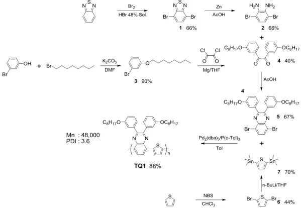
Synthesis of monomer intermediates and target polymer TQ1
Synthesis of comonomers
Synthesis of NDI copolymers
Synthesis of P(NDI2SiC6-T2) and P(NDI2SiC6-TVT)
List of Table
Introduction
Semiconducting polymer
Among n-type materials, especially with PDI (perylene diimide), NDI (naphthalenediimide) for having a unique tetracarboxyl diimide structure has been widely studied for the application of strong electron accepting unit and the resulting donor (D)-acceptor (A) type copolymers have been assessed as leading candidates. Due to its strong electron withdrawing ability, NDI derivatives have been adapted to n-type characteristic materials from small molecules to polymeric semiconductors.
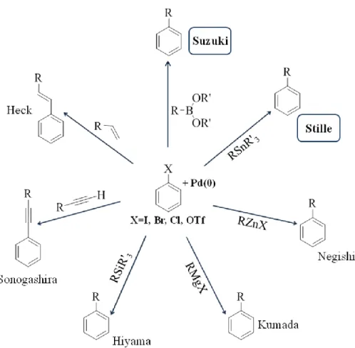
Palladium-catalysed reaction for Carbon-Carbon bond formation
This reaction shows high tolerance of many different functional groups and is considered one of the most effective aryl-aryl coupling methods. The Stille reaction is one of the most powerful reactions widely used for C-C bond formation with organotin compounds.
High-Efficiency Polymer Solar Cells with a Cost-Effective Quinoxaline Polymer through Nanoscale Morphology Control Induced by Practical
Abstract
Introduction
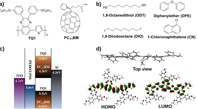
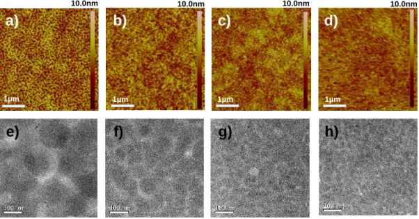
In this contribution, we comprehensively studied the effect of various solvent additives (1,8-octanedithiol (ODT), 1,8-diiooctane (DIO), diphenyl ether (DPE) and 1-chloronaphthalene (CN)) on the BHJ PSCs on TQ1: PC71BM. The techniques of X-ray diffraction (XRD), atomic force microscopy (AFM), and transmission electron microscopy (TEM) were applied to study the influence of CN on the nanomorphology and crystallinity of TQ1:PC71BM blend.
Results and Discussion
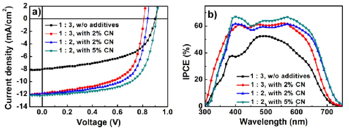
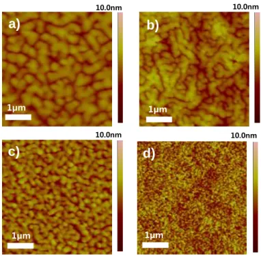
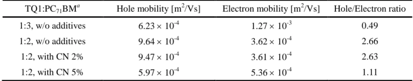
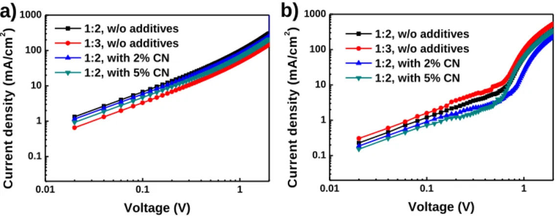
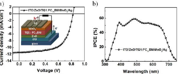
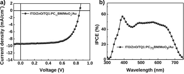
The representative current density-voltage (J-V) characteristics of the devices under the illumination of simulated AM 1.5G conditions (100 mW/cm2) are shown in Figure 2.3 (see Figure 2.4) and the parameters are summarized in Table 2.1. In the case of the blend films without CN, the hole mobilities (h) are generally an order of magnitude lower than the electron mobilities (e).
Conclusions
Experimental Section
These samples were transferred to a vacuum system (about 10-7 Torr) and an Al electrode (100 nm) was deposited on top of the BHJ layer. Then, a thin layer of MoO3 film (~5 nm) was evaporated on top of the active layer. Measurements were made with the solar cells in the glove box using a high-quality optical fiber to guide the light from a solar simulator equipped with a Keithley 2635 A source.
The device structures of the hole-only and electron-only devices are ITO/PEDOT:PSS/TQ1:PC71BM/Au and FTO/TQ1:PC71BM/Al, respectively. The space charge limited current (SCLC) mobilities were estimated using the Mott-Gurney square law JSCLC = 9(εrε0μ)/8ⅹ(V2/L3), where εr is the dielectric constant of the material, ε0 is the permittivity of free space, L is the distance between the cathode and the anode , which corresponds to the film thickness, and V is the applied voltage. In order to optimize the performance as well as to investigate the reproducibility and trend of the devices in our study, we not only fabricated more than 500 devices, but also performed the experiments under strictly controlled conditions and using high-quality reagents.
Naphthalene Diimide Incorporated Thiophene-Free Copolymers with Acene and Heteroacene Units: Comparison of Geometric Features and
Abstract
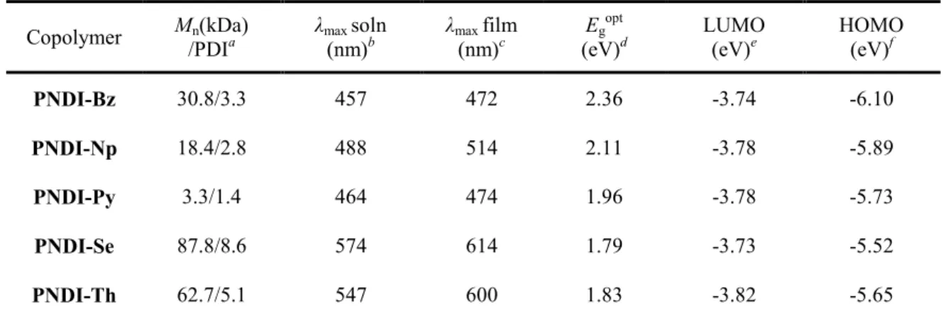
Naphthalene diimide incorporated thiophene-free copolymers with acene and heteroacene units: Comparison of geometrical features and. Interestingly, the best OFET performance is observed in centrosymmetric acene-based copolymer PNDI-Np cm2V-1s-1 despite strong electron donors towards efficient intramolecular charge transfer (ICT) when compared to those of other copolymers with axisymmetric unit. . Thus, the present work highlights that the geometrical features of the donors in NDI D-A copolymers strongly reflect the carrier mobility dynamics instead of introducing electron-rich moieties into the backbone to lower the band gap and further strengthen the ICT.
Introduction
Another practical way to increase the ICT in D-A copolymers having the same acceptor unit is to enhance the electron donating ability of the donor moieties. Thus, judging from the molecular design point of view, different thiophene-based moieties (e.g., different number of thiophene rings and modified thiophene derivatives providing different electron-donating power) as strong donor moieties within the main framework were predominantly introduced in constructing NDI-based copolymers D-A for applications in OFET.43-45. However, to date, there is no report on NDI-containing D-A copolymers based on the direct coupling of 'acenes' with moderate electron-donating properties. heteroacenes' as a thiophene analog with improved electron-donating properties compared to thiophene, which raises a number of very interesting questions: whether the empirical electron-donating ability of the donor companions matters.
What is the relative importance of counterpart comonomers other than their overall electron donating ability. Our studies on a structure-property relationship study of systematically designed NDI-based D-A copolymers with various acene and selenophene rings can provide answers to all these important questions. We hope that these studies, related to molecular packing, energetics, carrier transport and morphology in the family of the copolymer films, are significant by providing a timely analysis of NDI-based copolymers, to the rational design and synthesis of new, high - performance n-channel polymeric semiconductors, and promote their practical applications in OFETs.
Results and Discussion
These UV absorption characteristics of PNDI-Se and PNDI-Th reflect a stronger donating capacity of the heteroacene units. This calculation result means that the electron-donating ability of the donor co-units in NDI-based copolymers mainly affects the chromatic shifts and band gaps, possibly in the following order of the donating trend: Therefore, the electrochemistry and associated electronic structures of the NDI-based copolymers were based D-A copolymers investigated as thin films using.
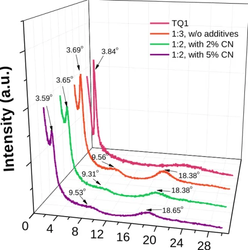
Despite the greatly extended degree of -conjugation length in the PNDI-Py basic unit, this geometry is suggested as an additional reason for its observed wider bandgap than that of copolymers containing single heteroacene units (Se and Th). The investigation of crystallinity and molecular organization in NDI copolymer thin films was analyzed by out-of-plane X-ray diffraction (XRD). The XRD patterns of annealed NDI-based polymer thin films are presented in Figure 3.8, and the XRD data are summarized in Story 2.3.
Conclusion
Experimental Section 1. Materials
After cooling to room temperature, the crude copolymers were precipitated from ammonia solution-methanol (100 mL:700 mL) and collected, followed by washing with methanol. The chloroform fraction was washed with saturated ethylenediaminetetraacetic acid (EDTA) solution, then the extracted chloroform fraction was concentrated by evaporation and reprecipitated in methanol. Fabrication and Characterization of OFETs: Bottom-gate top-contact OFET devices based on the NDI copolymers were fabricated on a heavily n-doped Si substrate with thermally grown 300-nm-thick SiO2 layer (Ci = 10 nFcm-2 ), where heavily n-doped Si and SiO2 layers were used as gate electrode and dielectric, respectively.
The surface of the SiO2/Si wafer was modified with n-octadecyltrimethoxysilane (OTS), as reported previously.57 After cleaning the SiO2/Si wafers with piranha solution (a 7:3 mixture of H2SO4 and H2O2), OTS solution (3 mM in) trichlorethylene) was spin-coated onto the SiO2/Si substrate at 3000 rpm for 30 s. NDI copolymers were dissolved in anhydrous chlorobenzene (~5 mg ml-1) and stirred at 80 °C for at least 12 h. The drop-casting method was chosen to produce thin films because the wetting ability of chlorobenzene solution is poor on the highly crystalline OTS-treated SiO2/Si substrate, and the drop-casting method tends to produce a higher crystallinity in the films.55,57 Drop-cast films were annealed on a hot plate at different temperatures (120 °C, 150 °C, 180 °C and 220 °C) for 30 min.
A Balanced Face-On to Edge-On Texture Ratio in Naphthalene Diimide- Based Polymers with Hybrid Siloxane Chains Directs Highly
Abstract
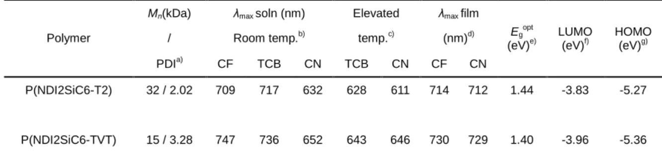
Balanced face-to-edge texture ratio in naphthalene diimide-based polymers with hybrid siloxane chains directs high. Although P(NDI2OD-T2) showed the best OFET characteristics with such facial textures,26 there have been several attempts to achieve its out-of-plane ordering, which would be expected to have better carrier mobility characteristics.27-29 However however, in previous reports, out-of-plane ordered structures in P(NDI2OD-T2) which can be obtained by lowering the surface energy by surface treatment and high temperature. A more recent study by Fabian and co-workers clearly showed that the orientation of several layers of P(NDI2OD-T2) obtained by the Langmuir-Schäfer method shows a low electron mobility of ~ 10-3 cm2/V∙ s relative to the face-on orientation (electron cm2/ V∙s). 28,31 These results challenge the traditional assumption that high carrier mobility is unequivocally related to high crystalline morphology of the edge orientation to obtain v -plane strong π-π stacking.29,32-36 Recently, the barrier to electron injection from the source/drain electrodes attributed to the vertically aligned long branched side chains (2-octyldodecyl solubilizing groups (2OD) ) having the same direction as the P(NDI2OD-T2) backbone is proposed as the main reason for the poor OFET characteristics in P thin film (NDI2OD-T2) directed to the edge.19.
In terms of this understanding, the best morphology to achieve high mobility and low Rc in P(NDI2OD-T2) is a mixture of face-to-face orientation in the contact region and edge-to-edge orientation in the channel region. Indeed, a remarkably enhanced electron mobility was reported for the polymer NDI (P(NDI2OD-TVT) containing (E)-2-(2-(thiophen-2-yl)-vinyl)thiophene (TVT) that co-exists with face-on and edge-on orientations 18, 19 In addition to molecular engineering of conjugated backbones, manipulation of side chains has recently been demonstrated to have a major impact on molecular packing, film microstructure and charge transport.2 ,3 ,37-39 Although currently there is a relatively large side.
Results and Discussion
In addition, increasing the temperature can trigger a continuous decrease in the proportion of polymers in the aggregate state. The optimized geometries and electron density distributions of NDI-based trimers were calculated at the B3LYP/6-31G* level (Figure 4.3). In both OFETs, Rc values gradually decreased as a function of elevated temperature.
First, information on the surface topography of the CF-fabricated films was obtained using atomic force microscopy (AFM) images. Thermal annealing of the cast films leads to slightly increased peak intensities at high incident angles (i.e. nominal with respect to the substrate). The coexistence of face-on and edge-on orientations in the CF-cast films is responsible for their higher electron transport mobilities than those of the corresponding CN-cast films.
Experimental Section 1 Materials
The reaction mixture was cooled to room temperature and extracted with water and chloroform. After the reaction, the solids precipitated by adding the reaction mixture dropwise to 800 ml of methanol were collected by filtration and then dried in a vacuum oven. The dried chloroform solution was concentrated under reduced pressure to precipitate the polymer in methanol.
After the conventional photolithography process of developing photoresist layer for source/drain electrode pattern, a 3 nm thick Ni adhesion layer and a 13 nm thick Au contact layer were deposited followed by photoresist liftoff. Note that the negative value of θ is presumably due to the gate field-enhanced mobility, which is compensated for by the conventional mobility damping. All spectra were processed using standard pre- and post-edge normalization methods, as described in previously published work.48 The pre-edge jump was subtracted to zero, followed by post-edge normalization, which consisted of dividing the pre -edge-normalized spectra. at the edge jump intensity achieved well above the C K edge beyond 320 eV.