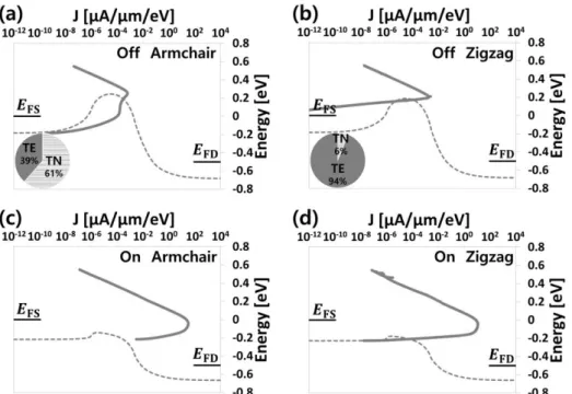
Transfer characteristics of the 10 nm gate length monolayer black arsenic and monolayer black phosphorus n-MOSFETs in the armchair and zigzag directions at VDS = 0.5 V. CB edge profiles along with the corresponding energy and current density transmitted from each valley for the 10 nm gate length monolayer black arsenic n-MOSFETs in the off state in the (a) armchair and (b) zigzag directions and in the on state in the (c) armchair and (d) zigzag directions. CB edge profiles along with the corresponding energy-resolved current densities for the 10 nm gate length monolayer black phosphorus n-MOSFETs in the off state in the (a) armchair and (b) zigzag directions and in the on state in the ( c ) armchair and (d) zigzag directions.
Transfer characteristics of the 10 nm gate length monolayer black arsenic and monolayer black phosphorus p-MOSFETs in the armchair and zigzag directions at VDS = -0.5 V. VB edge profiles along with the corresponding energy and current density emitted from each valley for the 10 nm gate length monolayer black arsenic p-MOSFETs in the off state in the (a) armchair and (b) zigzag directions and in the on state in the (c) armchair and (d) zigzag directions. VB edge profiles along with the corresponding energy-resolved current densities for the 10 nm gate length monolayer black phosphorus p-MOSFETs in the off state in the (a) armchair and (b) zigzag directions and in the on state in the ( c ) armchair and (d) zigzag directions.
Transfer characteristics of 7 nm gate length monolayer black arsenic and monolayer black phosphorus (a) n- and (b) p-MOSFETs at VDS = 0.5 V and −0.5 V in the armchair and zigzag directions, respectively. CB edge profiles and current density transmitted from each valley for 7 nm gate length monolayer black arsenic n-MOSFETs in the off state in (a) armchair and (b) zigzag directions. VB edge profiles along with the corresponding energy and current density from each valley for 7 nm gate length monolayer black arsenic p-MOSFETs in the off state in (c) armchair and (d) zigzag directions.
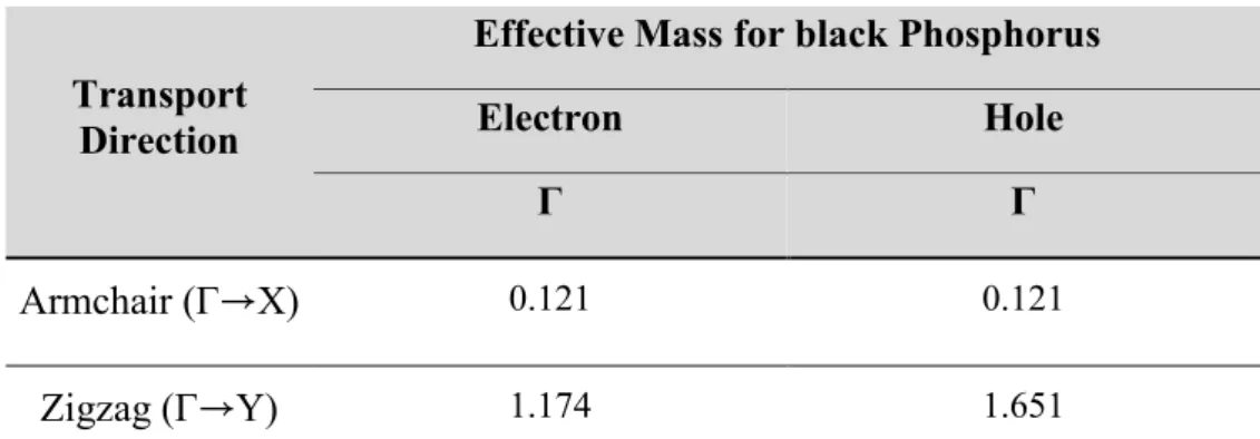
Effective electron and hole masses of monolayer black arsenic in the Γ and Δ valleys in the armchair (Γ→X) and zigzag (Γ→Y) directions.
Introduction
Methods
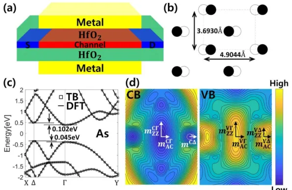
DFT simulation. DFT simulations by OPENMX [21] are performed to study the electronic band structures of monolayer black arsenic using the linear combination of pseudoatomic orbital method with
Ballistic Transport Simulation. To simulate the ballistic carrier transport of the device, we first use OPENMX [21] to obtain the TB basis set through maximally localized Wannier functions (MLWFs)
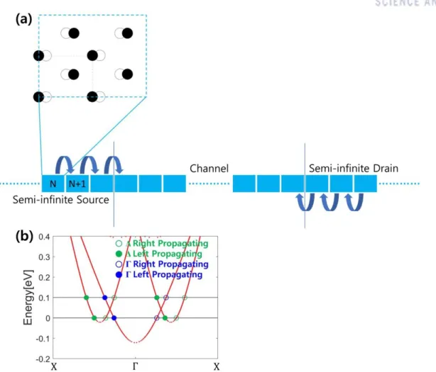
The direction of mode propagation can be determined by calculating the current from each mode. The current per energy mode between any two transport units N and N+1 can be obtained from. The current calculation for each mode can also be useful for identifying the propagation modes that belong to a particular valley, as it tells the group velocity of the mode.
We use the group velocities and wave vectors of the appropriate propagating modes to determine the valley where each mode resides. For example, at the 0.1 eV energy level in Fig. 2(b) , the group velocities of the right propagating modes are higher for the Δ valleys (green empty circles) than for the Γ valley (blue empty circle). At the 0 eV energy level, two right-propagating modes from the Δ valleys (empty green circles) have larger absolute values of the wave vectors than that from the Γ valley (blue empty circle).
By following these procedures, current can be calculated selectively for each valley. a) Device configuration of DG monolayer black arsenic MOSFETs with the HfO2 gate oxide thickness TOX = 3 nm and the channel length LG ≈ 10 nm. A unit cell (transport unit cell) used in transport calculations of monolayer black arsenic MOSFETs oriented in the armchair direction and schematic representation of modes propagation in the device.
Results and Discussion
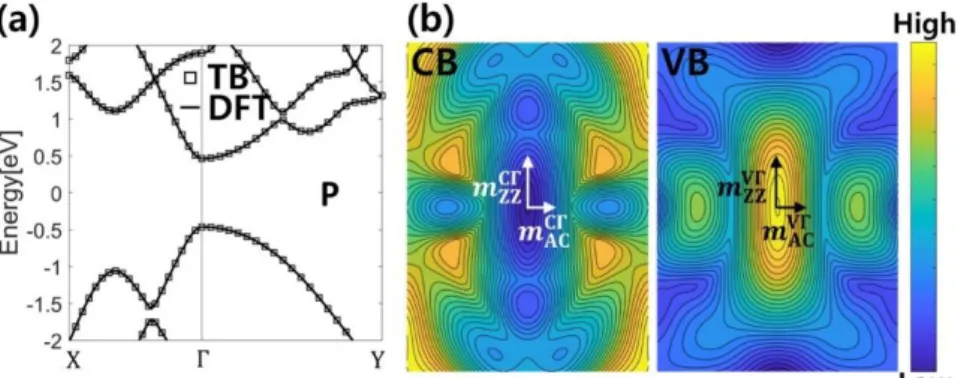
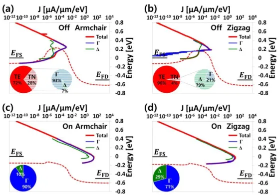
Effective electron and hole masses of monolayer black phosphorus in the Γ valley in the armchair (Γ→X) and zigzag (Γ→Y) directions. a) Band structures of monolayer black phosphorus. In the off state in Figure 5(a) and (b), IOFF consists of the tunnel current directly from the discharge source (TN) as well as the thermionic emission (TE) current in the monolayer black arsenic-based device for both transport directions. As seen in the pie chart representing the TN current valley composition in IOFF, the Γ valley (dashed blue) mainly supplies (~93%) the TN current while the Δ valley (dashed green) only contributes ~7.
In the zigzag direction (Figure 5(b) ), on the other hand, the Γ valley current density (blue) under the potential barrier becomes negligible due to the heavy transport effective mass. Single-layer black arsenic p-MOSFETs provide ION ≈ 4308 μA/μm in the armchair direction and 2000 μA/μm in the zigzag direction. The armchair direction gives the highest TN current in IOFF, but it is effectively suppressed in the zigzag direction as in Figure 9.
For the n-MOSFET in Figure 10(a) , the SS of the monolayer black arsenic degraded to 89 mV/dec and 84 mV/dec in the armchair direction and zigzag direction. On the other hand, the case of monolayer black phosphor, the SS deteriorated the most (104 mV/dec) in the armchair, but still showed good SS value (69 mV/dec) in the zigzag direction. For the p-MOSFET in Figure 10(b), the clear dependence of SS on the transport direction is confirmed in the case of the black arsenic-based device.
SS are significantly degraded in the armchair direction (116 mV/dec), but the rate of degradation in the zigzag direction is minimal (72 mV/dec). For single-layer black phosphor p-MOSFETs, SS is about 95 mV/dec in the armchair direction and about 67 mV/dec in the zig-zag direction. According to previous papers [25, 26], scaling has a stronger effect on monolayer black phosphors in the armchair direction for n- and p-MOSFETs due to the increased tunneling current below the potential barrier.
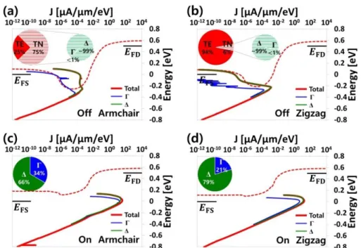
This not only makes the ratio of the TN current (~73%) higher, but also has a worse SS than in the zigzag direction. Therefore, most of the IOFF (~99%) arises from the TN current (dashed red), as seen in the pie chart. In the monolayer black arsenic-based device, the TN current from the Γ valley has a similar dependence on the transport direction in both n- and p-MOSFETs, which has a high TN current in the armchair direction and a low TN current in the zigzag direction. .
Decent SS is still possible in monolayer black phosphorene MOSFETs by tuning the transport direction in the direction of the heavy transport mass of the valley Γ. VB edge profiles along with the corresponding energy and current density transmitted from each valley for single-layer 7 nm gate-length arsenic p-MOSFETs in the off-state in (c) armchair and (d) zigzag directions.

Conclusion
Thickness-Modulated Semiconductor-Enabled Field-Effect Transistors at the Arsenic Transition Metal,” Scientific Reports.