Introduction
Terahertz wave properties
Because these photon energies are lower than the band gap energies of non-metallic materials, THz wave has properties to be absorbed in metal and penetrate insulator. Therefore, THz imaging system can be used in the industrial fields of security, food inspection, process control and biotechnology [4-7], which is safe for human body or bio-specimens due to its low and non-destructive radiation power compared to X- beam imaging (~ 10 keV).
Photonic approaches and its limitation
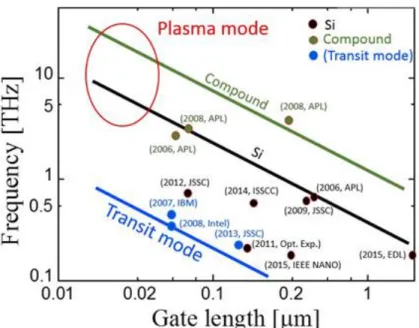
Electronic approaches: Plasma-mode vs. conventional transit mode
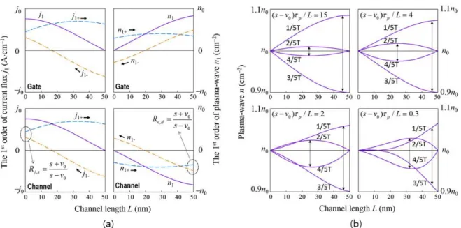
Using this theoretical analysis of the plasma wave in the channel, Figure 2-2 (b) describes that the resonant quality of the plasma wave is determined by (s−v0)p/L. To investigate the radiation effect of R-PWD, it is important to consider the correct resonant plasma wave behavior in the channel.
Plasma mode: Resonant vs. non-resonant mode
Motivation
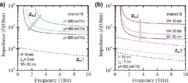
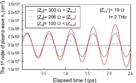
It should be noted that a sharp increase in |Zd,c| is due to physical properties of plasma wave in the R-PWT channel. On the contrary, it is obvious that plasma wave resonance cannot arise by itself when < 0.
Theory of resonant plasma-wave transistor (R-PWT)
Introduction
This chapter will shed light on the theory of R-PWT considering plasma waves, addressing the assumption of sv0 for analyzing material with relatively low channel mobility (section 2.2) and finite drain impedance |Zd| to ensure the realistic possibility of R-PWT (section 2.3). It will also be introduced how to evaluate the radiation power of R-PWT by deriving a power equation combined with the plasma wave and point charge dipole theories (Section 2.4).
Resonance phenomena in PWT
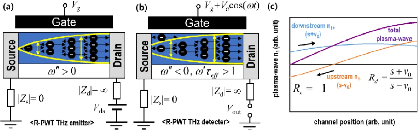
The estimated waveforms of the first harmonic plasma wave n (= n0+n1) in the same PWT channel in Fig. n1+ (downstream) at the boundary of the drainage channel is also reflected and transformed into n1− (upstream) in the channel (bottom right one of Fig.
Influence of finite drain impedance on R-PWT
The finite drain impedance allows the downstream plasma wave (n1−) to pass through the drain side so that reflection occurs less than infinity |Zd| matter. Therefore, insufficient amplitude comes to the drain side, so higher |Zd| should be required for sufficient reflection to occur plasma wave resonance.
R-PWT THz emission
Next, the vector potential can be obtained by considering the displacement current between floating gate and suspended channel, which results in. Although the validity of the power equation (detailed in Chapter 2.5) has been leading, the insufficient emission power of R-PWT motivates to invent a new PWD structure . A floating gate R-PWD with suspended channel (FG SC-PWD), as part of its effort, shows mW scale radiation power, which will be discussed in Chapter III.
R-PWT THz detection
- Effective momentum relaxation time for plasma-wave
- Review on reported V out equations
- Wavenumber considering low and sv 0 condition
- General resonant V out equation
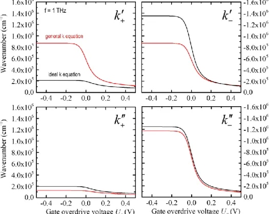
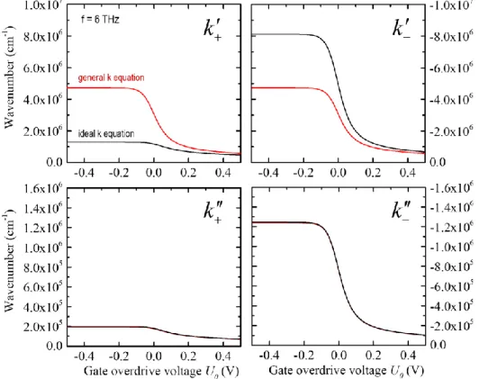
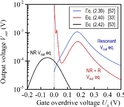
Also, to make R-PWT with low channel mobility, it is necessary to achieve short channel length for resonance. It is clear that Eq.(2.44) must be taken into account in the evaluation of Vout and its related equations to explain the entire range of gate voltages. 2.45) explains that there is voltage component to determine plasma wave velocity axis. It is noticeable that there is the shift of resonant peak to higher gate voltage compared to reported Vout equations (Eq.
This means that it is important to consider both v12 and integral v0 terms in Vout equations to investigate the low channel mobility R-PWT showing sv0 tendency.
Summary
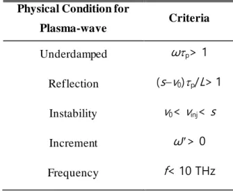
It should be noted that the physical state of plasma wave reflection is (s−v0)p/L. gt; 1 is viewed in the design window. This new physical state that explains the degradation of the plasma wave amplitude can be represented as Lack of electrons in the channel hinders the formation of temporal and spatial collective oscillations (i.e. plasma waves).
Finally, based on the design window of the R-PWT, I reported experimental evidence of plasma wave resonance in strained Si channel FET.
Theory of Floating gate R-PWD with suspended-channel (FG SC-PWD)
Structural limitation of PWT
The conventional plasma wave theory has been adopted as a plasma wave transistor (PWT), which has the 2-dimensional electron gas (2DEG) formed by the gate terminal of the conventional FET structure. Because of that, PWT has a fundamental problem of electron mobility deterioration of the gate field and surface roughness spreading as well as reduction of the electron charge density by gate leakage current through the thin gate oxide. Moreover, when an ideal 2D material such as graphene is inserted under the gate as a channel, the original high mobility deteriorates significantly [56-57], so the implementation of PWT based on conventional FET whose channel is controlled by the gate has serious performance limitation as THz emitter and detector.
Therefore, in this chapter we take an approach away from the conventional transistor operation, which forms and controls the 2DEG channel at the gate, and propose a new THz plasma wave device structure where the channel is not controlled by the gate.
Device structure of FG SC-PWD
Resonance phenomena in FG SC-PWD
- Influence of finite drain impedance on FG SC-PWD
- Radiation power of FG SC-PWD
The emission of THz EM wave from FG SC-PWD has the same mechanism as R-PWT so it is possible to evaluate its radiated power by Eq. In the case of FG SC-PWD, there is no bias gate voltage, which means that each device characterized by its channel length has a narrow operating frequency regime, or it is necessary to use additional reverse gate voltage. The radiation power of FG SC-PWD decreases as frequency increases, since shorter channel length has higher resonance frequency and contains fewer electrons in the channel area.
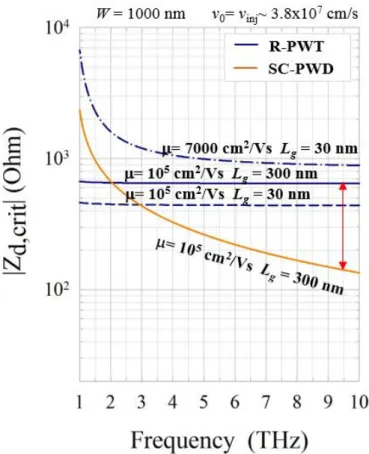
This definition of critical impedance makes it possible to analyze FG SC-PWD more accurately.
Summary
4-7 (b), the increment of vinj shows the strong dependence on plasma wave velocity as shown in Fig. Using these theoretical expectations, it was first introduced that plasma wave resonance can occur in the channel of Si R- PWT with several evidences. Kim, “Physical Analysis and Design of Resonant Plasma Wave Transistors for Terahertz Emitters,” IEEE Trans.
Ryzhii, “Modulation Effects of Photocarriers on the Terahertz Plasma Wave Resonance in High Electron Mobility.
Design window of R-PWD
Introduction
By modulating the plasma wave velocity of Eq. 3.5) for the downstream flow, the basic equation of the s-v0 line is given by. Since a high eff means less damping of the plasma wave amplitude, a criterion that combines eff with the resonant frequency of the plasma wave () (i.e. eff >1) is useful to judge the possibility of R-PWT THz detection. Valusis, “Current-driven resonant plasma detection of terahertz radiation: Towards Dyakonov-Shur instability,” Appl.
Kim, “Feasibility and design of resonant terahertz emitters based on nanoscale strained silicon plasma wave transistors with enhanced mobility,” Jpn. Fay: Direct electrical observation of plasma wave-related effects in GaN-based two-dimensional electron gases, Appl. Kim, “Extended Design Window of Plasma Wave Resonant Transistor for Terahertz Emitter Considering Degenerate Carrier Velocity Model with Fermi-Dirac Scattering,” Jpn.
R-PWT design window
- Physical conditions of R-PWT
- Consideration of source injection velocity
FG SC-PWD design window
Summary
In contrast, the non-resonant phenomenon is only excited by the external THz signal, which causes the plasma wave to initiate from the source side when the ideal state (Cgd > Cgs) is reached. These experimental data showed that plasma ripple occurs in the R-PWT channel, which is confirmed by three evidences: the first is that a high quality factor eff >1 is ensured. In order to verify the possibility of R-PWD for different materials, I proposed a design window concept that takes into account both plasma wave theory and electronic device theories.
Valusis, "Slanted mode effect on terahertz plasma wave resonant detection in InGaAs/InAlAs multichannel transistors", Appl.
Si R-PWT THz detector
Introduction
Based on the design window for Si R-PWT, which shows that resonant THz detection is possible even at leff = 20 nm (see Figure 5). Then, the experimental results are presented, and theoretical proofs guarantee resonant THz detection with Si technology. a) Si R-PWT 3D design window considering the source injection rate as a variable, showing the resonance window as THz emitter. These graphs imply that resonant THz detection (and even emission) is possible through optimization (Figures 4-5 and 4-9 are reused).
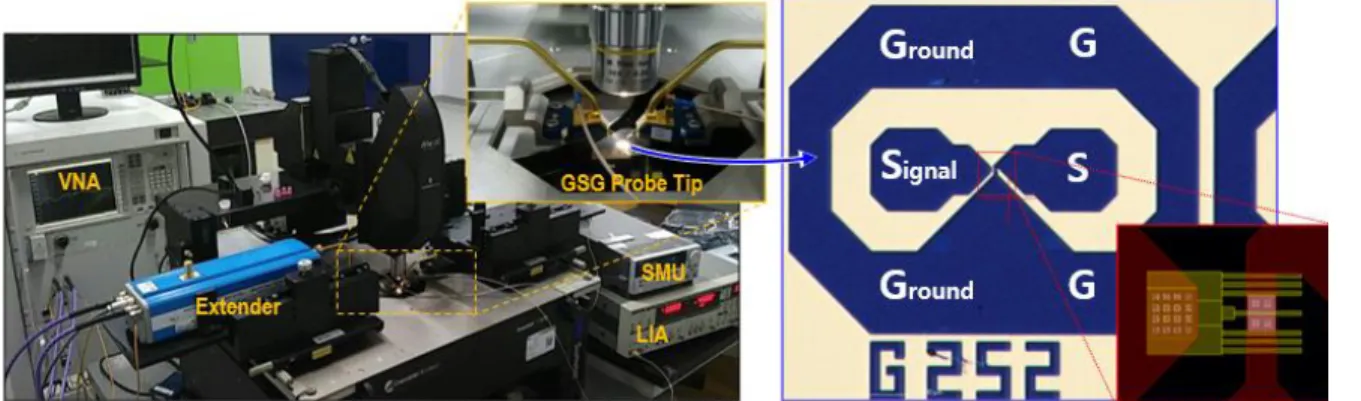
Device structure and experimental setup
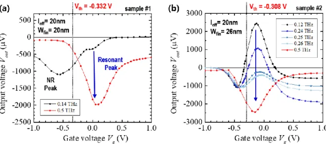
Before measuring Vout, using lock-in-amp (LIA), two Id-Vg curves were measured continuously using the source meter unit (SMU). As expected by non-resonant theory, NR peak appears when Cgs < Cgd or Cgs > Cgd. One example of NR peak characteristics (leff= 335 nm), useful for analyzing resonant peak, related to (a) Iout, (b) Vout and (c) capacitance.
Lock-in-amp also reads Vout as absolute value, so it shows positive Vout sign in the panel.
Experimental evidence for resonant THz detection
- High quality factor of eff >1
- Resonant V out peak placed above threshold voltage
- Non-linear increment of V out peak
The main difference between resonant and non-resonant mode is that the resonant phenomenon occurs in the strong inversion state of MOSFET as plasma wave should propagate and make multiple reflections in the channel. The highest Vout peak of non-resonant plasma wave loses its amplitude by increased plasma wave velocity, which means that the wave gradually becomes close to the drain side as Vg increases. In this case, If the quality factor is higher than unity with the achievement of edge conditions, it is possible that the amplitude of plasma wave increases again, and its peak is placed at the point that resonant frequency coincides with external THz frequency.
The other is that experimental results of fTHz in sample 2 show unclear increasing trends to explain nonlinear increase compared to theoretical Vout using Eq.
Summary
테라헤르츠 연구에 대한 조언도 많이 해주셨어요. 저도 성호와 오랫동안 연구실에서 일했는데, 성호와 함께 연구를 시작했고 지금은 조금 다른 주제를 연구하고 있습니다. 여러분의 지원에 감사드립니다.
가끔 테라헤르츠 연구에 대해 이야기 나누는 것이 큰 도움이 되어서, 깊은 감사의 말씀을 전하고 싶습니다.
Remaining work to be done
Conclusion