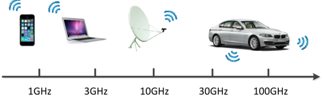
Introduction …
Signal generator develop motivation
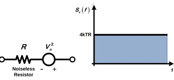
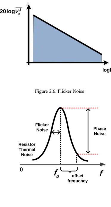
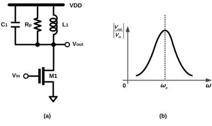
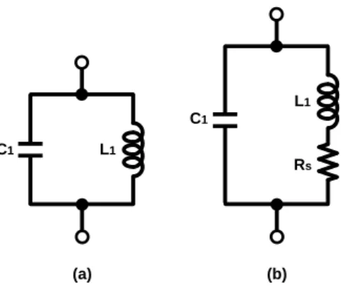
As shown in Fig. 2.3(a), the impedance in the LC circuit is maximum when an imaginary number is 0. Sv f kTR f (2.7) The given equation is proportional to the absolute temperature T and shows the regular value up to 100 THz as being lower from the higher frequency. The oscillation frequency of the circuit shown in fig.2.10 is determined by the resonance frequency of the inductor and capacitor.
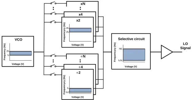
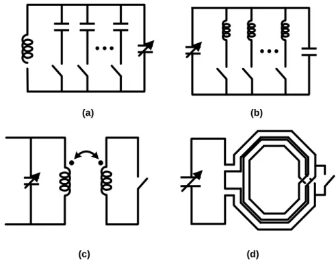
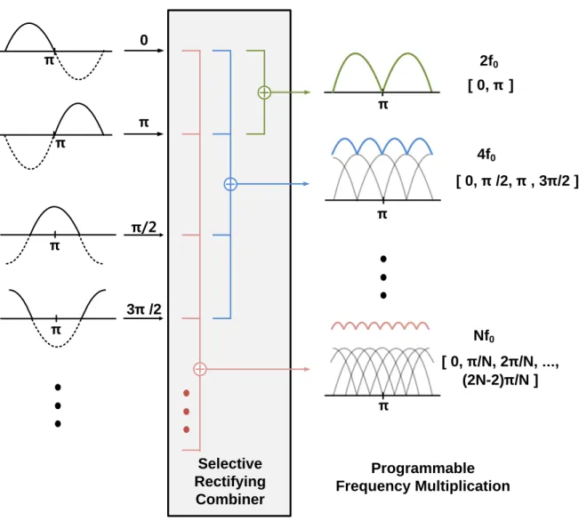
The second circuit, shown in fig 2.12(a), provides discrete tuning through the multiple array and switches of the capacitor. The third circuit, shown in fig 2.12(b), provides discrete tuning through the multiple array and switches of the inductor. So, this section contributes an explanation about the external structure called as "Frequency Multiplier". The frequency multiplier is the circuit that uses linear superposition of sinusoidal signal.
If the differential phase (0,π) signals are superimposed at a node, which is called "linear superimposition", the signal generates dual frequency signal, and the results are presented in [13]. This structure using the connecting wire inductor is difficult to make the structure of the inductor in the way shown in fig 2.11.
Design the Ultra Wideband Signal generator
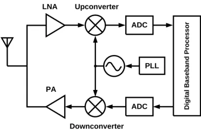
The Basic of RF transceiver
Oscillation Principle of LC Oscillator
- LC resonance frequency
- Phase Noise in CMOS environment
However, the real impedance generates an irregular signal of oscillation frequency due to the inductor resistance and capacitance. The performance of the inductor and capacitance can be expressed in a Q value (quality factor) and the equation is given by. So the analysis should be done considering the series resistance of the inductor.
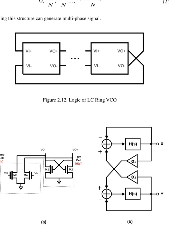
The article refers to the combination of the inductor and the capacitor as LC Tank and explains various ways to tune frequencies through the combination, as shown in Figure 2.11. The fourth circuit, as shown in 2.12(c), uses mutual induction and changes the oscillation frequency by varying the impedance during switching. The previous chapter mainly describes the design process of the oscillator and the frequency tuning process with changing the structures of the LC tank.
Once N phase of the same frequency signal is generated using LC ring type VCOs, there are two times (2X), four times (4X), …, N times (NX) more frequencies. So, using the operational characteristic, this structure of programmable frequency multiplier can cover the whole frequency bandwidths for wireless communication. So here, using VCO structure with PMOS, not the structure of the gmcell which is widely used, a circuit of a 4 stage LC ring type is designed.
The outputs of 4-stage LC ring type VCOs are connected to each frequency multiplier by a switch. Depending on SW1-SW3 values, polyphase outputs from the LC ring VCO are selectively connected to the frequency synthesis block. The VCO structure with amplifier cell made only in NMOS is also designed instead of the VCO using NMOS and PMOS cross-coupled pairs.
The maximum eightfold (8X) wideband characteristic is measured differently from the result of the previous version of signal generator with programmable wire bond inductor VCO. The structure design that the paper proposes is shown in fig 4.1, the design is designed with the quadrature type[20] made of two main VCOs, which consists of the two small VCOs designed in an in-phase structure. The paper deals with the design of an Ultra-wideband signal generator and the concepts of the VCO, the most important device for the design of a signal generator.
Design consideration of the signal generator
- MOSFET Non-ideality
- Wideband oscillator
- Theory of the frequency multiplication
- LC Ring type VCOs
Proposed Ultra wideband signal generators
- Signal generator with programmable wire bonding inductor VCO
- Signal generator using reconfigurable selective combination
Based on this principle, this chapter explains an ultra-wideband signal generator that can cover all existing wireless frequency bands. A picture of the die is shown in Figure 2.23, where the multiphase LC ring signal generator and its selective rectifier combiner have been fully integrated. Each unit. Each VCO unit uses one symmetrical helical coil for its LC tank, and the entire signal generator includes four integrated inductors placed symmetrically to reduce mismatch between VCO units.
It means that most existing frequency bands up to 60 GHz could be covered by the combination of this proposed work and the previous low-end multiplexing technology. But since the LC tuning range of the VCO core is narrow, the multiplied frequency range is wide. However, the frequency multiplier is used for the VCO core, so the signal generator will not work if the VCO core is missing. Therefore, designing a signal generator using a new type of structure of VCO and a frequency multiplier can support the entire existing wireless frequency bandwidth.
All the processes to design the schematic with a cadence tool, to lay out with a virtuoso tool and to fabricate with the TSMC 65 nm process are used to obtain experimental results, which leads to the design of a wideband signal generator which can generate at most 6 Broadband frequency bandwidth -60 GHz. The first version of the signal generator, the wire-type signal generator using the concept of linear tunable overlap was proposed and experimentally verified to extend the existing limit of wideband signal generator technology. Also, if this signal generator includes conventional CMOS frequency dividers, which are known to work well in the prototype VCO frequency range, it can cover all existing frequency bands below 30 GHz.
The results suggest the feasibility of designing a more powerful wideband signal generator and a more complete version of the ultra wideband signal generator through continued efforts of additional research. a) Schematic of a varactor diode (b) Capacitance-voltage characteristic of an NMOS device.
Experimental results
Experimental environment
Results of Signal generator with programmable wire bonding inductor VCO
- Frequency band width of signal generator
- Output spectrum & Phase noise of signal generator
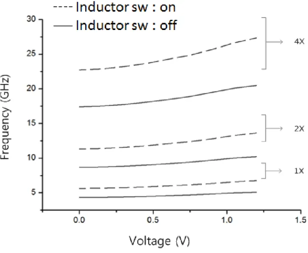
The frequency bandwidth results obtained by the experiment are shown in Figure 3.2. The graph of the adjustable frequency bandwidth of the VCO core structure using the inductor switching with the bond wire is the VCO core (1X), and the number can be doubled (2X) or quadrupled (4X) with a programmable frequency multiplier characteristic. The reason why the graph is missing the octal (8X) frequency is that it is difficult to design a chip in a symmetrical structure due to the wire-bonded inductor structure and to create multiphase unless a symmetrical structure is designed.
Due to the difficulty of oscillating at the default frequency, increasing the inductance of the inductor by applying equation 2.13 generates a frequency lower than the default frequency. Through the method of changing the shape of the bond wire inductor, the most stable state capable of oscillation is achieved.
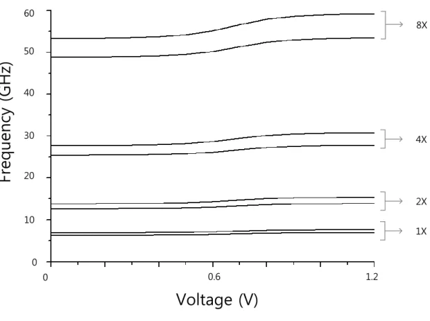
Results of Signal generator using reconfigurable selective combination
- Frequency band width of signal generator
- Output spectrum & Phase noise of signal generator
The signal from the VCO core is 1X frequency which is not measured because the output ports of the VCO core are not designed. Accordingly, the VCO core frequency and the core frequency can be assumed by applying the equation for diving double (2X) frequency by two. This work was compared with previous works in Table I, where it can be known that this work would be one of successful broadband design methods.
In order to feasibly provide double (2X), quadruple (4X) and N-fold (NX) frequency bandwidths in the frequency multiplier, the frequency bandwidth of VCO core must be twice the oscillation frequency. This paper is to explain and propose the structure of such a VCO as an alternative. The small VCOs structured in-phase determine Z-value using transformer inductor and change the direction of the current to control mutual inductance, as much as to provide wideband frequency bandwidths [21].
In addition, the two large VCOs designed in the quadrature-type structure can, through a reconfigurable method, generate two- or four-phase signals. By using such a structure together with the multiple array cap structure, the multiphase quadrature broadband VCOs can be designed using the transformer inductor, which are possible to generate at least twice the frequency bandwidth than the oscillation frequency. It involves understanding LC resonance, the minimum gm of MOSFET, phase noise and how to minimize the phase noise and design method.
Finally, the understanding of the concept of frequency multipliers, which is the most important contribution of this paper, leads to the design method of such a multiplier, which gives the understanding of how to generate the core VCO (1X), double (2X), quadruple. Frequency bandwidth (4X),… and N-fold (NX) applying a programmable structure. With a four-stage LC ring VCO and a programmable frequency synthesis circuit, the concept of tunable linear overlap was implemented, which can provide programmable frequency multiplication. If LC tank circuits are modified to include multiple sets of variable capacitors as in [2-3], the entire frequency range from 5 GHz to 30 GHz would be covered continuously.
A reconfigurable frequency synthesis structure was proposed and experimentally verified to have a very wide frequency response of 660 GHz and also to have optimal power consumption which is adaptively optimized for different operating modes . Considering that CMOS frequency dividers are working well below 6 GHz, this work is supposed to be one of the significant advances for supporting all existing wireless frequency bands up to 60 GHz. VCO using NMOS and PMOS coupled pairs. a) Schematic of VCO using NMOS and PMOS coupled pairs, (b) Current flow through the floating resonator when M1 and M4 are on.
Future Works
New Structure of VCOs
Conclusion