I certify that this project report entitled "IMPLEMENTATION OF VLSI DESIGN FLOW FOR MIPS-BASED SOC" prepared by LEE ZHAO MIN has met the required standard of submission in partial fulfillment of the requirements for the award of the Bachelor of Engineering (Hons) Electronic Engineering at Universiti Tunku Abdul Rahman. The copyright of this report belongs to the author under the terms of the Copyright Act 1987 as qualified by the Intellectual Property Policy of Universiti Tunku Abdul Rahman. Due acknowledgment must always be given to the use of material contained in or derived from this report.
Loh Siu Hong for his invaluable advice, guidance and his immense patience throughout the development of the research. The MIPS design is optimized to reduce design cost and improve design performance.
INTRODUCTION
IC design
In this era, design automation is used to assist with the stages of the VLSI design flow. Electronic design automation (EDA) tools can support the engineers in the chip manufacturing process, such as planning, design, verification and other phases (Gianfagna, 2021). In the late 1960s, the first EDA tool was created to optimize device placement on a printed circuit board (Kahng et al, 2011).
The EDA equipped with programmed circuit synthesis function and which can automatically steer the design became dominant in the market by the 1990s (Kahng et al, 2011). Some of the major EDA software companies in the market include Mentor Graphics, Cadence Design Systems and Synopsys (Kahng et al, 2011).
CPU architecture
The continuous development of transistor downsizing is pushing the chip to its physical limit (Takahashi, 2005). The abstract interface between software and hardware at the lowest level, which consists of a machine language program that includes all essential information to ensure the correct execution of the program, is known as an instruction set architecture (ISA) or architecture (Patterson and Hennessy, 2014). . One method is to increase the number of things an instruction must do, and another method is to decrease the number of instructions used to perform a particular function (Abd-El-Barr and El-Rewini, 2005).
For example, Pentium from Intel, PowerPC from IBM & Macintosh and MC68000 from Motorola are some of the machines that use the CISC approach (Abd-El-Barr and El-Rewini, 2005). The design must be synthesis with complete timing constraints to ensure the functionality of the chip after manufacture.
LITERATURE REVIEW
- CISC architecture
- RISC Architecture
- MIPS architecture
- RICS and CISC comparison
- MIPS instruction
- R-type
- I-type
- J-type
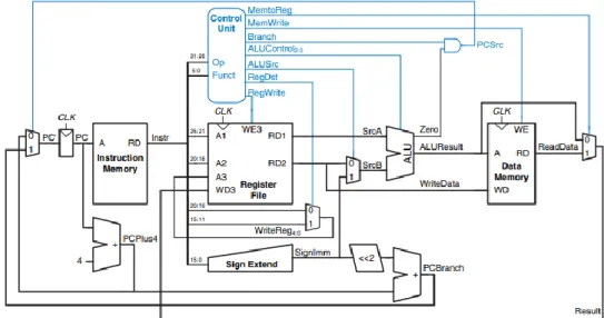
- Type of MIPS Microarchitectures
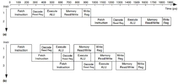
- Single-cycle microarchitecture
- Multicycle microarchitecture
- Pipelined microarchitecture
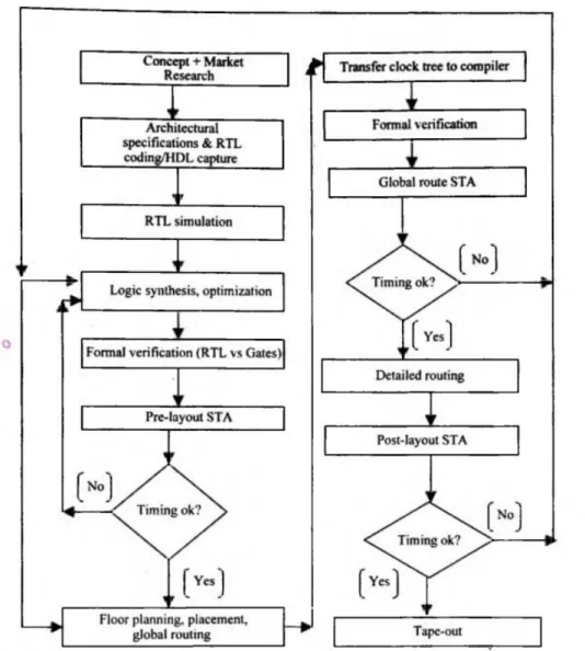
- VLSI design flow
- Digital design using HDL
- Logic synthesis
- Physical design
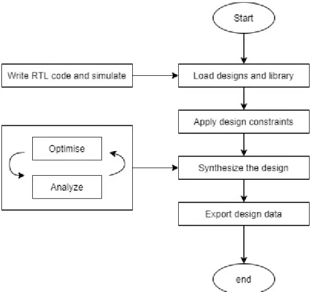
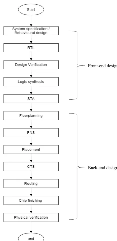
Concept and market research is the first step in the VLSI design flow to identify the product's competitiveness in the market. After providing RTL netlist functionality, the next stage in VLSI design is logic synthesis. At this stage, the calculation of the estimated design schedule is performed to verify the validity of the schedule (Kishore and Prabhakar, 2009).
The cell library used in the logic synthesis process and the algorithm of the synthesis tool will largely define the quality of the output (Kishore and Prabhakar, 2009). The final step in physical design is to verify the functionality of the design (Das, 2010).
METHODOLOGY
- VLSI Design Methodology
- Front-end design
- Register Transfer Level (RTL) Design
- Logic Synthesis
- Static Timing Analysis
- Back-end design
- Floorplanning
- Power Network Synthesis
- Placement
- Clock Tree Synthesis
- Routing
- Chip Finishing
- Physical Verification
- Design Tools
- Synopsys Design Compiler
- Synopsys IC Compiler
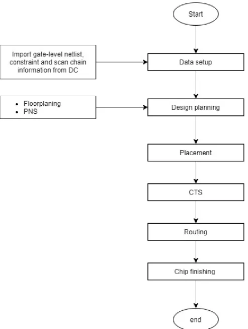
Design constraints, such as constraints and time constraints, come from the design. The gateway level netlist is designed and optimized in terms of performance, speed, power and area depending on the design constraints. STA is performed to check for timing violations in the design to determine if the design meets the timing constraints.
Power rings and power belts are created at this stage to form a power network and ensure sufficient power throughout the design. Therefore, the voltage drop from the current pads in the center of the design can be reduced. Sufficient space is reserved for routing during automatic placement as required by the stated routing constraints to ensure design patency.
The IC Compiler provides the automatic routing function to facilitate the routing process for a large number of nets in the design. The tool will try to drive the design in the least amount of timing, DRC and LVS violations. Timing analysis, DRC and LVS of the design are checked after each of the insertion steps to ensure that the design has no violations.
The design must be verified to be free of DRC and LVS violations before exporting the GSDII file using the tape out tools. The Design Compiler (DC) can be invoked using two interfaces which are the interactive shell, the DC shell, and the interactive graphical user interface (GUI), Design Vision. The DC shell is the command line interface of the design compiler while Design Vision provides a graphical visualization such as schematic generation.
RESULTS AND DISCUSSIONS
Design Verification
- Design Compilation and Simulation
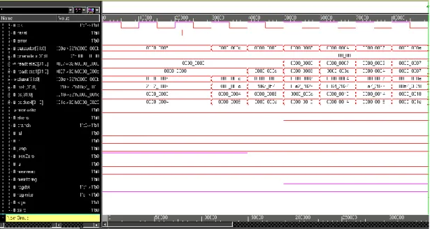
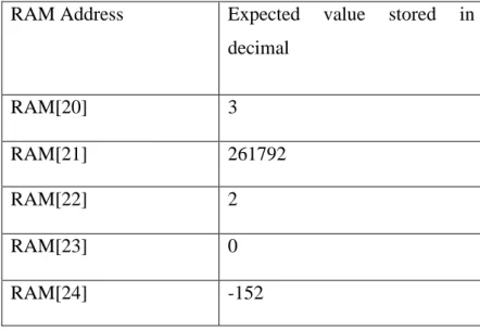
With branching taking place in cycle 12, both instructions are proven to work correctly under specific conditions. The SW (Cycle 16) stores the calculation result of ADD and SUB to be verified through the test bench. Based on Figure 4.1, it is verified that the value loaded into the data memory and the memory address are the same as the expected result, demonstrating the correct operation of the instructions from cycles 1 to 16.
The next cycle is to load the result stored in data memory in the last cycle to be used for a series of operations starting from cycle 18. In cycle 25, the final result of the calculation from cycles 18 to 23 is stored in data memory and verified test bench use. For cycles 26 to 28, the new initial values are loaded into the register to be used later for rotary operations.
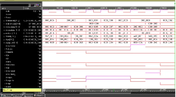
In cycle 31, two registers with unequal values are used for BNE and branching occurs in the next cycle. In cycle 38, the program branches to execute SRA, SLL, and SRL via execution of BLEZ. As shown in Figure 4-6, no branch should be taken in the next cycle to prove that the statement functions correctly, since it will only branch for Rs greater than Rt.
The calculation result of SRA, SLL and SRL is stored in the data memory and verified to have the correct output in cycle 47. For cycles 48 and 49, NOR is performed and the result is again stored in data memory to be tested. Since JALR is the last instruction in the program, the JR will jump to load 0 into instruction memory as the sign for the end of the program as shown in Figure 4.6.
Logic Synthesis
- DC Setup and Design Translation
- Design Checking before mapping and optimization
- Analysis of Timing, Area and Power before Mapping
- Mapping and Optimization of Design
- Analysis of Timing, Area and Power after Mapping and Optimization
- Design Checking after Mapping and Optimization
- Output Gate-level Netlist
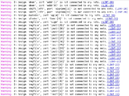
This is to check the hierarchy issues and connectivity of the design. It is because the design is currently a generic technology (GTECH) netlist which is technology independent. The pre-optimization design area statistics and information are generated as shown in Figure 4.17.
For Synopsys DC, the mapping and optimization is performed based on the constraints applied to the design. The tool is used to automate the process of mapping and optimize the design with the help of the algorithm. A gate-level netlist corresponding to the constraints applied to the design is generated using the logic gates of the library.
The tool modifies design meshes, cells, and gates to meet design requirements. The clock frequency applied in the design is about 294 MHz which is equivalent to a clock period of 3.4 ns. The tools had modified elements in the design to meet the constraints applied to it.
So you can ignore the warning to ensure the design works properly after mapping and optimization. Since the networks are not connected to any ports, this will not affect the functionality and connectivity of the design. Before printing the port-level netlist, the plan is checked against the constraints applied to it.
Physical design
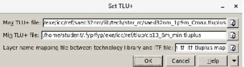
- ICC Setup and Gate-netlist import
- Floorplanning
- Placement, CTS, and Routing
- Chip Finishing and Tape Out
The setting to create the floor plan and the summary of the floor plan is as shown in Figure 4.38. By applying the setting, the tool automatically generates an optimum area based on the design as shown in Figure 4.39. The PNS is executed using the GUI and the setting is as shown in Figure 4.45.
A summary of the placement optimization, as shown in Figure 4.52, shows that the plan has a dwell time violation with 3098 paths. First, a short map of the critical area is created using the tool as shown in Figure 4.62. Similarly, an open critical region map with a maximum threshold of 1 is created, as shown in Figure 4.63.
The QoR report is also generated to examine the latency performance of the final layout, as shown in Figure 4.73. Then the power analysis of the final design is done based on the power report as shown in Figure 4.72.
Conclusion
At the same time, the setup time performance is slightly improved to the margin of 0.09 ns. However, the power dissipated by the design becomes larger due to the increase in net switching power in physical design. The high frequency of the clock used in the design increased the switching power.
In addition, the large number of registers used in the design for RAM and ROM contributed to the high power consumption. In conclusion, the power performance of the design has been scaled down to optimize timing performance.
Recommendation
The margin can be improved by adjusting the timing constraints applied to the design during DC. Memory elements designed as macrocells can be individually optimized to achieve better timing and power performance. In the current model, RAM and ROM are optimized as a group with other submodules.
This causes the register to dissipate a lot of power and results in an overall high power consumption. By generating macrocells for RAM and ROM, they are individually optimized with specific power limits applied to them. Thus, the power consumed by the RAM and ROM can be reduced, resulting in a lower power loss of the overall design.
Macro cells can be created using another EDA tool from Synopsys called Memory Compiler. This results in the design not being able to connect to other devices via external pins. Whereas in a pipelined design, a single-cycle processor is divided into multiple stages to execute instructions concurrently.
Available at: