RFID SIMULATION IN MATLAB I SIMULINK
by
KHAlRUL.IKHWAN BIN RAMLI
Dissertation submitted in partial fulfillment of thereqtrirementforthe
Bachelor of Engineering (Hons) (Electrical & Electronics Engineering)
JUNE2008
Unversiti Teknologi PETRONAS Bandar Seri Iskandar
31750 Tronoh Perak Darul Ridzuan
Approved by,
CERTIFICATION OF APPROVAL
RFID SIMULATION IN MATLAB I SIMULINK
by
Khairul Ikhwan Bin Ramli
A project dissertation submitted to the Electrical & Electronics Engineering Programme
Universiti Teknologi PETRONAS in partial fulfilment of the requirement for the
BACHELOR OF ENGINEERING (Hons) (ELECTRICAL & ELECTRONICS ENGINEERING)
UNIVERSITI TEKNOLOGI PETRONAS TRONOH, PERAK
Jnne2008
CERTIFICATION OF ORIGINALITY
This is to certifY that I am responsible for the work submitted in this project, that the original work is my own except as specified in the references and acknowledgements, and that the original work contained herein have not been undertaken or done by unspecified sources or persons.
KHAIRU ANBINRAMLI
ABSTRACT
Nowadays, Radio Frequency Identification (RFID) applications are widely used in daily application and also in industries. RFID is an automatic identifications method, relying on storing and remotely retrieving data using devices called RFID tags or transponders. The RFID tag is an object that can be placed into a product or person for the purpose of identification using radio waves. RFID uses wireless communication technique, found application in many areas such as attendance tracking system in campus or in a big factory and also for inventory tracking and management. In this project, the work of Yifen Han, Qiang Li and Hao Min from Auto-ID Labs at Fudan University, Shanghai, China will be reproduced so that further simulation result can be generated. Special attention is emphasized on the development of transmitter, receiver, wireless channel and tag for the system simulation environment because these four elements are the most important subsystems to produce an RFID simulation environment. This project will evaluate the system performance by changing the coding method and operation distance. At this point, half of transmitter subsystems have been done. The subsystems developed so far are source coding, raised cosine Hilbert and digital to analog converter.
ACKNOWLEDGEMENT
I would like to thanks my coordinator, Puan Salina Mohamad for giving me an opportunity to take part in the final year project. My involvement in the project has significantly shaped my vision in the real world of electrical and electronic engineering and also gave me confidence to go out and face the world. I would also like to thank my supervisor, Puan Norashikin Binti Yahya for giving continuous guidance and great ideas from the beginning to the end of this project. Her remarkable contribution in this project is highly appreciated. Thanks to all my friends that support me in the process of completing this project.
TABLE OF CONTENTS
CERTIFICATION I
ABSTRACT. ii
ACKNOWLEDGEMENT iii
CHAPTER I: INTRODUCTION 1
1.1 Background of Study • 1
1.2 Problem Statement 2
1.3 Objectives and Scope of Study 2
CHAPTER2: LITERATURE REVIEW AND THEORY. 3
2.1 Model of transmitter 4
2.2 Model of receiver 13
2.2 Model of tag . 15
2.2 Wireless channel 17
CHAPTER3: METHODOLOGY . 18
3.1 Project activities 18
3.2 Tool/Equipment required 19
CHAPTER4: RESULTS AND DISCUSSION 21
4.1 Project progress 21
CHAPTERS: CONCLUSION AND RECOMMENDATION 27
5.1 Conclusion 27
5.2 Recommendations 27
REFERENCES
28
APPENDICES 29
LIST OF FIGURES
Figure 1: General Building blocks ofRFID ... 3
Figure 2: Model of Transmitter. ... .4
Figure 3: Block diagram ofl-Q imbalance on Simulink ... 6
Figure 4: Configuration for SSB, DSB and Return Link ... 6
Figure 5: Example ofNRZL coding method ... 8
Figure 6: Impulse response of raised-cosine filter with various roll-off factors ... 9
Figure 7: Frequency response of raised-cosine filter with various roll-off factors ... 9
Figure 8: Model of Receiver ... .13
Figure 9: Model ofTag ... 16
Figure 10: Methodology of the project.. ... 18
Figure 11: Source coding subsystem ... 21
Figure 12: NRZL coding ... 22
Figure 13: Raised cosine Hilbert subsystem ... 23
Figure 14: Output of raised cosine Hilbert filter. ... 23
Figure 15: Digital to analog subsystem ... 24
Figure 16: Output on scope 1.. ... 25
Figure 17: Output from quantizer ... 25
Figure 18: Output analog low pass filter. ... 26
LIST OF ABBREVIATIONS
RFID Radio Frequency Identification
UHF Ultra High Frequency
SSB
Single Side BandDSB
Double Side BandASK
Amplitude Shift KeyingPSK
Phase Shift KeyingFIR
Finite Impulse ResponselSI
Intersymbol InterferenceAM
Amplitude ModulationSNR
Signal to Noise RatioDAC
Digital Analog ConverterOSR
Oversampling RateLO
Local OscillatorPA
Power Amplifiervco
Voltage Controlled OscillatorLNA
Low Noise AmplifierLOS
Line of SightAWGN
Additive White Gaussian NoiseFCC
Federal Communications CommissionNF
Noise FiguresDSP
Digital Signal ProcessingBER
Bit Error Rate1.1 Background of Study
CHAPTER1 INTRODUCTION
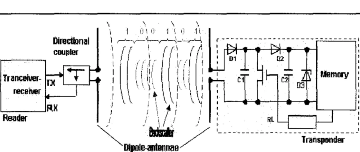
Ultra High Frequency (UHF) RFID system consist two main parts which is a reader and a tag. The reader part contains transmitter and receiver and a card is usually used as an RFID tag. For a simple analysis, a single reader and a single tag bi-directional communication can be investigated to reveal the physical parameters. The communication link used is a half duplex which means reader to tag and then tag to the reader at a time but not simultaneously. For the forward link, the reader sends a modulated carrier to the tag and powers up the tag. The tag arbitrates it state and determines tag respond to reader. In the return link, once reader sends a continuous wave carrier, the tag will receives the carrier for power supply and backscatters by changing the reflection coefficients of antenna. In other word, data is sent to reader from tag. Besides backscattering technique, the load modulation technique also can be used to reflect the wave from the tags to the reader. In general, backscattering technique is used in the far field, whereas load modulation applies in the near field, within a few wavelengths from the reader. This project will construct a system model of the forward link and return link based work done by the Yifeng Han, Qiang Li and HaoMin.
1.2 Problem Statement
Performances of RFID systems are affected by the coding method, parameters used in the simulation building block and also the operation distance. To evaluate the system performance ofRFID systems, we will varies the coding method in the transmitter block, parameters used in the transmitter and receiver block as well as the operation distance between the tag and reader.
1.3 Objective and Scope of Study
This project involves developing the reader, transmitter, tag and wireless channel using available blocks from communication library, radio frequency library, signal processing library and simulink library it self in Simulink. Some of the blocks, such as modulation depth control unit, continuous carrier and double side band (DSB) are not available in the Simulink and has to be created using S-function.
CHAPTER2
LITERATURE REVIEW AND THEORY
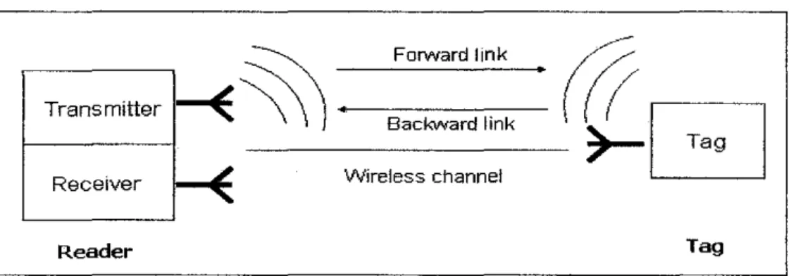
RFID system consists of three main blocks as shown in Figure I which are reader, tag and wireless channel. The reader consists of transmitter and receiver. Antenna is important in RFID application because it is used for transmitting and receiving the signal. In this simulation work, transmitter block, receiver block and tag block is produced separately. In forward link, the transmitter sends the modulated carrier to the tag. So it is difficult to see whether the transmitting signal is under the frequency mask of the local regulation. Therefore the raised cosine filter, Hilbert transform, digital to analogue converter (DAC) and filter, phase locked loop (PLL), non-ideal mixer and high power amplifier are added. There are three transmission types can be selected; single side band (SSB), double side band (DSB) and continuous wave carrier. The free space is modeled by pass loss with phase changing due to distance between the reader and tag. Additive White Gaussian noise (A WGN) channel is added to model the noise source from space.
~~
Forward link(((
Transmitter
Backvvard link Receiver
~
Wireless channelr-G
Reader Tag
Figure I: General building blocks of RFID
2.1 Model of Transmitter
Raised Cosine Hilbert Up Conversion
' ' ' '
DAC Smooth Filter
High Power Amp iller
~--- Band Pass Filter! Antenna
Phase LockEd Loop (Pll)
, \
'
' - -
IIQ Imbalance DSBISSBIC\N switch
Data Processing
1 ze:v-J:J:Er
!.. -,!.!g~----
Figure 2: Model of Transmitter
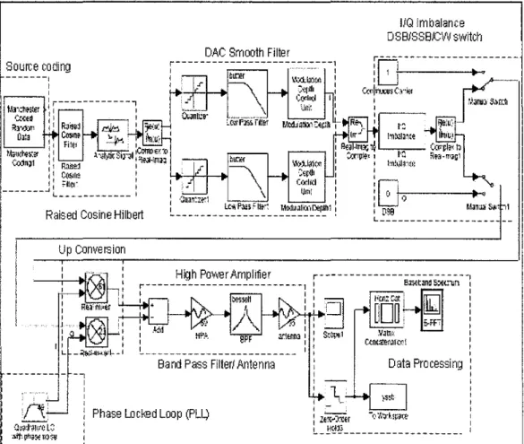
The architecture of the transmitter shown in Figure 2 is chosen to be inphase I quadrature (I-Q) branches for the reason of the single side band (SSB) transmission and different modulation method such as amplitude shift keying (ASK) or phase shift keying (PSK). I-Q imbalance is used to create complex baseband model of signal impairments caused by imbalances between in-phase and quadrature receiver components [l]. Typically, these are caused by differences in the physical channels for the two components of the signal.
Consider the conversion of a single tone at RF to baseband. Ideally, the I and Q outputs of the receiver are
I(t)
=
cos(mt) and (1)Q(t)
=
sin(mt), (2)respectively [2]. Here, OJ is the baseband frequency of the tone. In contrast, a realistic direct conversion receiver produces;
I'(t) = acos(mt) + fJ1 (3)
Q' (t)
=
sin(mt +If/)+ fJQ (4)where If/ is the phase error, which is assigned to the "Q" path, a IS the magnitude error, which is assigned to the "I" path, and fJ1 and fJQ are the DC biases associated with each path.
The I-Q imbalance block applies amplitude and phase imbalances to the in-phase and quadrature components of the input signal, and then combines the results into a complex signal. Commonly, mismatch levels around 1 - 5 % in amplitude and 1 - 5 degrees in phase are stated feasible or realistic [3]. The block diagram of I-Q imbalance subsystems is shown in Fig. 3. The steps taken to perform the I-Q imbalance are as follows;
1. Separates the signal into its in-phase and quadrature components.
2. Applies amplitude and phase imbalances, specified by the I/Q amplitude
imbalance (dB) and I/Q phase imbalance (deg) parameters, respectively, to both components.
3. Combines the in-phase and quadrature components into a complex signal.
4. Applies an in-phase de offset, specified by the I de offset parameter, and a quadrature offset, specified by the Q de offset parameter, to the signal.
Amplitude Phase Imbalance Imbalance
de Offset
Fig 3: Block diagram ofi-Q imbalance on Simulink [I]
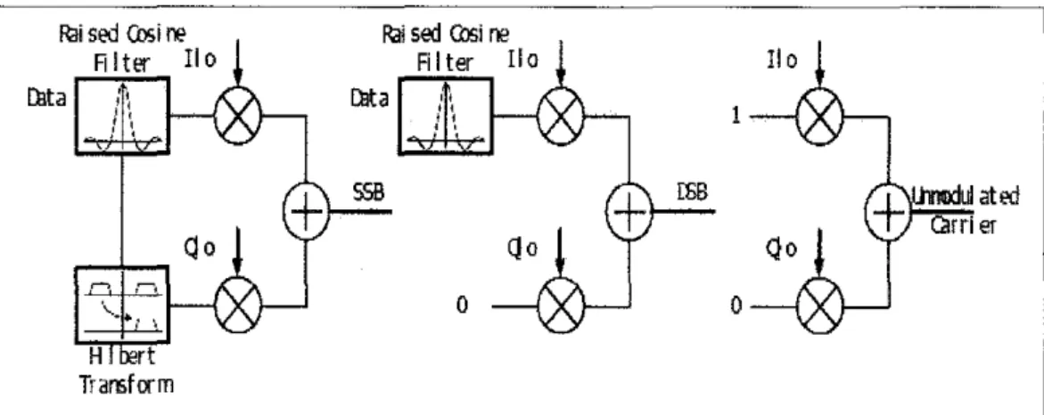
The coding method used for forward link is Non Return Zero Level (NRZL) Coding. The transmitter should fulfill the protocol and support the double side band (DSB) or SSB transmitting for forward link send an un-modulated carrier for return link.
R3i sed Cllsi re Riter Ilo l:llta
H rt Transform
Poi sed Cllsi ne Filter Ilo Dll:a l \ " "
0 0
Figure 4: Configuration For SSB, DSB and return link
Figure 4 shows the configuration of transmitter for different modulation schemes. It shows that the SSB modulation scheme is produced when both data from raised cosine filter and Hilbert transform are mixed together with the
existence of 1-Q imbalance. If there is no output data from raised cosine filter, the DSB modulation scheme is produced with the existence of 1-Q imbalance.
Lastly, the unmodulated carrier is generated when there is no output from both raised cosine filter and Hilbert transform. The transmitter model in Simulink consists of interconnection of these blocks:
1. Coding
2. Raised Cosine Filter 3. Hilbert Transform 4. Quantization 5. Up Converter
6.
Power Amplifier7. Output Band Pass Filter
Detail of these block will be explain in the next session
2.1.1 Coding
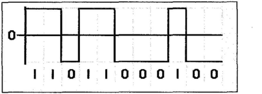
For this project, the protocol is based on using Non Return Zero Level (NRZL) coding for source coding block in transmitter architecture. The NRZL is one of the line coding used in the communication system. The NRZL is the binary code which is "Is" represents one significant condition and "Os" are representing another significant condition. Compare to the return zero (RZ) coding method, this NRZL don't have the rest state. The pulses of this NRZL also have more energy than RZ coding method. The example of the NRZL coding method is shown in Figure 5.
.
-
0
.' - -
I I 0 I I 0 0 0 I 0 0
Figure 5: Example ofNRZL coding method
2.1.2 Raised Cosine Filter
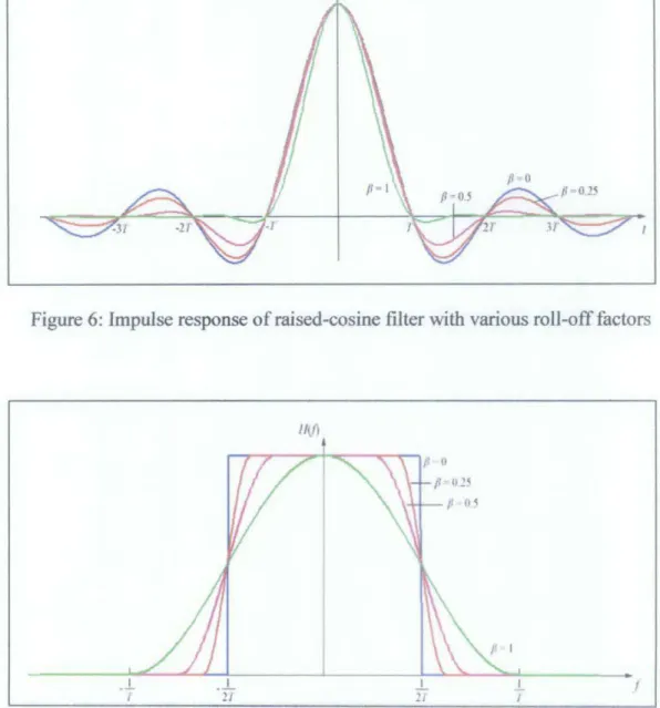
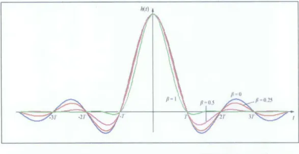
Data transmission over bandlimited channels requires pulse shaping to eliminate or control intersymbol interference (lSI). Raised cosine filters are Nyquist filters use to provide lSI-free transmission [4]. The output of the filter is strictly bandlimited signal. This is desirable since it reduces the interference the modulated signal creates for uses in adjacent channel bands. It allows a communication system to signal at a rate near the Nyquist rate for the channel bandwith without the excessive sidelobe filtering which can cause channel distortion and intersymbol interference (lSI). The impulse response, h(t), is given by
(5)
and the frequency response of the filter is given by
T,
If/~ 1-P
2T
h(t)
= T[l+cos(:n:T[/!/-1-P]JJ 1-P </f/~1+P
2
p
2T ' 2T 2T (6)0, otherwise
where
f3
is the roll-off factor which determines the bandwidth of the pulse shape with values between 0 and I. The plot of impulse response and frequency response for various value ofp
is shown in Figure 6 and Figure 7 respectively.h{t)
Figure 6: Impulse response of raised-cosine filter with various roll-off factors
• .!.
I .!.
I
Figure 7: Frequency response of raised-cosine filter with various roll-off factors
The graphs show the amplitude response as
p
is varied between 0 and I, and the corresponding effect on the impulse response. As can be seen, the time- domain ripple level increases asP
decreases. This shows that the excessbandwidth of the filter can be reduced, but only at the expense of an elongated impulse response. Asp approaches 0, the roll-off zone becomes infinitesimally narrow so the impulse response approaches to an ideal or brick-wall filter.
2.1.3 Analytic Signals and Hilbert Transform
Hilbert transformer is considered as an all pass filter which shifts the phase of its input signal by 90° [5]. The impulse and frequency responses can be formulated as
{ -j, HHT(f)= .
],
f~O
f<O
(7)
(8) Hilbert filters can be used to construct signals with only positive frequency content. These kinds of signals are generally termed as analytic and always have complex value.
The elimination of the negative frequencies can more generally be formulated as follows. Given an arbitrary signal x(t), the complex signal is in the form of
x(t)+ jx8r(t) (9)
where xHr(t) denotes the Hilbert transform of x(t). In this case, the spectrum of complex signal is
X(f)[l+ jHHT(f)] (10)
where
. {1+
j(-j), 1~0{2,
1~01+JH (1)- -
HT - 1 + j(j),
I
< 0 - 0,I
< 0. (11)Equation (11) shows that the original negative frequency content has been eliminated.
2.1.4 Quantization
After digital signal processing, the digitized signal is send into analog part. In practical converting digital to analog using, a digital analog converter (DAC) will introduce convert digital quantization error. In this work, the signal is oversampled by FIR filter such as raised cosine and Hilbert transform, the clock of DAC is usually higher than the signal. In an oversampling circuit, the maximum sinusoidal power to the quantization noise [6] is;
where
SNRm.,. = 6.02N + 1.76 + 10log(OSR)
N is number of quantization bits, OSR is oversampling rate,
SNR is signal to noise ratio.
(12)
The first term in (12) is the signal to noise ratio (SNR) due to the N-bit quantizer while the OSR term is the SNR enhancement obtained from oversampling. This can model the noise power induced by the DAC. The low pass filter after DAC is to smooth the waveform and lower the high order harmonics.
2.1.5 Up Converter
The transmitter architecture of Figure 2 suffers from local oscillator (LO) pulling [7] due to the noisy output of PA that corrupts VCO spectrum. The output power of power Amplifier (PA) is a modulated waveform with high power and a spectrum centered around the LO frequency. Despite of various shielding techniques employed to isolate the voltage controlled oscillator (VCO), the "noisy" output of the PA still corrupts the oscillator spectrum through "injection pulling" or "injection locking" whereby the frequency of an oscillator tends to shift towards the frequency of an external stimulus[8]. The problem worsens if the P A is turned on and off periodically to save power.
Therefore, the VCO must be followed by a buffer stage with high reverse isolation between the VCO and the PA.
2.1.6 Power Amplifier
The power amplifier is modeled with nonlinearities for these types of power amplifiers. The AM/PM effect of amplifier is not included since tags are not sensitive to the phase of the carrier. The power amplifier is to give a proper power gain and the gain range of the power amplifier should cover the regulatory of CEPT, FCC, etc.
2.1. 7 Output Band Pass Filter
The output band pass filter is to remove the out of band spurious spectrum. A fourth order Bessel filter is selected with the bandwidth range from 860MHz to 960MHz. The maximum input power of the filter is about 1 W and it can be implemented by passive elements.
2.2 Model of Receiver
Free Space
<:.\T.:IT~:~ Tag Reflection
---~~~---
Figure 8: Model of Receiver
Model of receiver shown in Figure 8 are built from the combination of these blocks in Simulink :
1. Antenna
2. Low Noise Amplifier (LNA) 3. Direct Conversion
4. Fifth order Butterworth filter
5. Base-band Digital Signal Processing
2.2.1 Antenna
The antenna can be configured in two types, two antennas or one antenna with a circulator. In return link, the receiver of reader listens to the response of tag while the transmitter sends a continuous wave to power up the tag. It is very critical to have a high isolation between transmitter and receiver for a high performance reader.
The direct coupling from transmitter to receiver with one antenna is larger than two antennas because of low isolation performance of circulator.
Assume the transmitting power is 36dBm (FCC), the isolation of a circulator is about 35dB (Commercial circulator can hardly exceed 40dB). Therefore the power seen in the receiver is about OdBm. In this case, the receiver circuit should have a large dynamic range to handle the relative large signal and detect the weak signal backscattered from tag. The direct coupling signal is much larger than the reflection from the enviromnent and the enviromnent can be ignored.
2.2.2 Low Noise Amplifier ( LNA)
The LNA is optional for different antenna configurations. If it is configured with two antennas, the isolation is relative high. In this case, LNA is used to get a proper gain and better noise factor NF of receiver. The gain range is from -10 dB to 10 dB. If a circulator is used, the isolation is very poor and the power into the receiver is very large. In this case, a power splitter is used instead ofLNA because of its capability of handling large signal.
2.2.3 Direct Conversion
The architecture of receiver is direct conversion receiver suitable for multi-protocol operation. The DC offsets are very large due to low isolation between the transmitter and receiver. The receiver will have a multi stage gain to amplifier the weak signal. Since the DC offset is much larger than the signal, the offset may saturate the amplifier if it is not removed. An ac coupling stage is inserted after the mixer filtering out the DC component.
2.2.4 Fifth Order Butterworth Filter
A high order charmel select filter is applied to get a sufficient out of band suppression. The filter type in the receiver is a 5-order Butterworth filter due to it flatness in the passband and suitable for amplitude modulation
2.2.5 Baseband Digital Signal Processing
The baseband DSP is to decode the signal from analogue to digital converter (ADC). The DSP should combine the signal power of 1/Q branch for maximizing the signal power to get the best bit error rate (BER) performance.
2.3 Model of Tag
There are three general varieties of RFID tags, active, passive and semi- passive. Passive tags require no internal power source, so this tag only active
when a reader is nearby to power them up. For semi-passive and active tag, they require an external power source such as small battery to power them up. For this project, passive tag is used. The tag is powered up by the modulated carrier send from the reader. Model of tags shown in Figure 9 consist of two parts:
a) Tag received Power b) Tag Reflection Model
Direction~!
coupler
Traoceilrer-ln;--l ....
~
recen.er I
':::--:-___JRX Reader
Figure 9: Model of Tag
2.3.1 Tag received power
In forward link, the output power is:
where:
PEIRP = PPAGTX
PEIRP is the effective isotropic radiated power, PPA is the power of power amplifier,
Grx is the gain of the transmitter antenna.
The power transmitted from reader to tag can be expressed as:
p"' = PPAGTXGtag(
4~ r
where:
P .-ec is the power received by tag ,
PPA is the power of power amplifier,
(13)
(14)
G rx is the gain of the transmitter antenna, G,ag is the gain of the tag,
A, is the wavelength of the carrier, d is the distance from reader to tag.
2.4 Wireless Channel
The wireless channel is modeled by the Friis transmission equation as shown in equation (15). RFID system is not a line of sight (LOS) communication system. In wireless channel model, the influence of reflection by the environment should be considered.
where:
P = P,G,G,)}
r (4nr)2 (15)
Pr
is the power measured at the receive antenna output port, P1 is the power measured at the transmit antenna input port,G
1 is the gain of the transmit antenna,Gr
is the gain of the receive antenna,A
is the wavelength of the carrier, r is the distance from reader to tag.CHAPTER3 METHODOLOGY
Project methodology had been divided into project activities and tool or software required.
3.1 Project Activities
I
Building the transmitter blockI
l
Find the Simulink block set that gives desired outputJ
I
Connect all the block setl I
I
Used appropriate parameters for the block setI
I
Build a M File S-Function for the appropriate block _\I
Run the simulation of Transmitter blockl I
t
I
Get simulation result for transmitter blockI
Figure 10: Methodology ofthe project
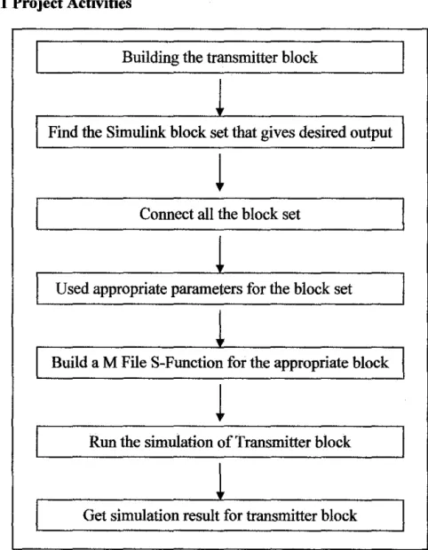
At the early stage, a study and research about an RFID communication system was done to understand its behaviors. After that, the transmitter architecture is developed using Matlab I Simulink. Before the whole transmitter architecture can be produced, the transmitter subsystems block need to be fmd in the Simulink such as analytic signal, quantizer, analog low pass filter and so on.
Unfortunately, there some subsystems block are not available in the Simulink such as modulation depth control unit. M files S-function need to be created in Matlab to produce this modulation depth control unit subsystem block. When some of the subsystem blocks have been identified, they are connected to each other to synchronize to produce a small system. The value of each parameters used in the blocks set must be carefully selected. The examples of parameters used are gain, amplitude, type of filter ,filter order and input type and so on.
3.2 Tool I Equipment Required
• Matlab
• Simulink
3.2.1 S-function
S-function is the System Function in Matlab which provide a powerful mechanism for extending the capabilities of Simulink [9]. S-Function allows users to add their own algorithms to Simulink model. S-function can be defined using M file in Matlab or C language code. S-functions are very useful tool in several situations and included in the Simulink library. An S-function represents a general Simulink block with the input vector, u, output vector, y, and state vector, x, consisting of continuous state, Xc and discrete state, xd. Every S-
function must include code to set the initial values of all elements of the state vector, and to define the sizes of the input vector, the output vector, and the continuous and discrete components of the state vector.
CHAPTER4
RESULT AND DISCUSSION
4.1 Project Progress
Some subsystems of the transmitter model is developed using Matlab and Simulink which involve using communication block library, radio frequency block library and signal processing block library. However there are certain blocks for transmitter architecture model are not in the Simulink library such as modulation depth control unit, so S-function m-files need to be created. The creation of block using S-function has not been successful. At this point, only source coding, raised cosine Hilbert and digital to analog converter subsystems have been done.
4.1.1 Source coding
IlJlt---rr=====~==:l~CJ~
Scope3 Pulse
Generator
~ Bernoulli
Binary
B~Hnoulli Binary Generator
Figure 11: Source coding subsystem
NRZL coding method is used as a source coding for this project. The subsystem is shown in Figure 11. The pulse generator produced the time based
pulse type. For the Bernoulli binary generator, the probability to produce a zero is 0.5, the output data type is double and the sample time is 1. Both output data from the blocks will be multiplied to produce the NRZL coding method. The output for this subsystem is shown in Figure 12. The NRZL coding has amplitude of 1, period of 2 second and 50% pulse width.
Figure 12: NRZL coding
4.1.2 Raised Cosine Hilbert
Bernoulli Bin1ry Gene,tor
Norm•l
R•lsed Cosine Aulytio Sign• I Tr•nsmit Filter
Figure 13: Raised cosine Hilbert subsystem
Soope1
The subsystem for raised cosine Hilbert is shown in Figure 13. The filter type for the raised cosine transmit filter is normal type. The roll off factor is chosen to be 1 and the upsamp/ing factor is 32. The filter gained is normalized. For the analytic signal block, the filter order is chosen to be 100 because the filter order must be in even number. The output for this subsystem is shown in Figure 14.
r - - - i ...... , . . . . . , . . . T - - - r ... ·:· . . ... : ... .
• <!. ••••
Figure 14: Output of raised cosine Hilbert filter
The output of raised cosine Hilbert filter is a bandlimited signal which is required in order to avoid lSI. Because of the group delay (numbers of symbols) is set to be 1, so it shown from the graph that there is a delay at the output from raised cosine filter with the data from zero order hold. The graph shows that the ripple is narrow because of the roll off factor value.
4.1.3 Digital to analog converter ( DAC)
Soopojj
Figure 15: Digital to analog subsystem
The subsystem for DAC is shown in Figure 15. For the quantizer block, the quantization interval is 0.5 and the sample time is -1.-1 is for inherited. The analog low pass filter used is an 8-order butterworth filter with passband edge frequency equal to 30 rads/sec. Figure 16 shows the real and imaginary components of the analytic block which perform Hilbert transformation. The output from quantizer block is in digital form as shown in figure 17.The output from the analog low pass filter block should be in analog form because of the filter characteristic .Figure 18 shows the output from analog low pass filter which is in analog form ..
Figure 16: Output on scope I
··r· -- ···r··---- -;--
... i ...
-~... .
Figure 17: Output from quantizer
···.··· ... ... ····:····-:···
.
.. .
. .
... . .
. .
. .
. . . . . ·.· ... -... .
. .
.
. . •j• ... ~ ... ~· ... ..
.. .
. . . . ::
:: : :
Figure 18: Output analog low pass filter
CHAPTERS
CONCLUSION AND RECOMMENDATION
5.1 Conclusion
The aim of this project is to evaluate the performance of RFID system by varymg the coding method and the operation distance. There will be some simulation result based on the evaluation criteria as the desire output of this project. In the first stage, the simulation model of transmitter being develops. Then, for the second stage, the simulation model for receiver, wireless channel and front-end of tag will be developed. At the final stage, all the simulation models of transmitter, receiver, wireless channel and front-end tag are combined together to produce an RFID system.
Based on the RFID system, some simulation results are produced.
5.2 Recommendation
Throughout this project, certain issues can be highlighted and improved.
Those issues are:
1. Students are required to have a strong background in Matlab/
Simulink especially utilizing S-function since the extension is really helpful in the simulation.
2. Each parameter of the subsystems blocks should be fully understands to avoid misunderstanding and yield better result.
REFERENCES
[1] The Mathwork
http://www.mathworks.com/access/helpdesk/help/toolbox/commblks/index.html?/ac cess/helpdesk/help/toolbox/commblks/ref/igimbalance.html&http://www.mathwork s.com/cgi-
binltexis/webinator/search/?db=MSS&prox=page&rorder=750&rprox=750&rdfreg
=500&rwfreg=500&rlead=250&sufs=O&order=r&is summary on= 1 &ResultCount
= 1 O&guery=ig+imbalance&submitButtonNarne=Search
[2] S.W. Ellingson, Correcting 1-Q Imbalance in Direct Conversion Receivers,
Technical Report, ElectroScience Laboratory, The Ohio State University, February 2003
[3] Peng Yan, Eero Maki-Esko, Mikko Valkarna, and Markku Renfors, Receiver Architecture, http:// www.invocom.et.put.poznan.pl/-invocon!materials.php [4] Ashok Ambardar, Analog and Digital Signal Processing, 2"d Edition
[5] Peng Yan, Eero Maki-Esko, Mikko Valkarna, and Markku Renfors, Bandpass and
Complex Signal and System Concepts,
http://www.invocom.et.put.poznan.pl/-invocon/materials.php, 5 May 2008
[6] David Johns, Ken Martin, "Analog Integrated Circuit Design", John Wiley &
Sons, Inc, 1997
[7] Behzad Razavi, "RF Microelectronics", Prentice Hall, Inc. 1998
[8] K.Kurokawa,"Injection Locking of Microwave Solid-state Oscillators, Proc. IEEE, vol.61. ppl386-1410", Oct 1973
[9] James B. Dabney, Thomas L. Harman, "Mastering Sirnulink 2", Prentice Hall, 1998
System Modeling and Simulation of RFID
Yifeng Han, Qiang Li, Hao Min
Auto-10 Labs at Fudan University, Shanghai, P. R. China, 200433 (han> f a'fudan.edu.cn, hgmng({t fudan.edu.cn, hmm a1tudan.t;dU.L:1)
Abstract
A system simulation environment in Matlab/Simulink of RFID is constructed in this paper.
Special attention is emphasized on the analog/RF circuit. Negative effects are concerned in the system model, such as phase noise of the local oscillator, TX-RX coupling, reflection of the environment, A WGN noise, DC offset, UQ mismatch, etc. Performance of the whole system can be evaluated by changing the coding method, parameters of building blocks, and operation distance. Finally, some simulation results are presented in this paper.
1. Introduction
UHF RFID system can be divided to two parts, readers and tags. Generally, an RFID system contains several readers and a large amount of tags in practical application. The collision problems of both tags and readers are resolved in the arithmetic [I] and MAC protocol [2].
For a simple analysis, a single reader and a single tag bi-directional communication can be investigated to reveal the physical parameters. The communication link is half duplex, reader to tag and then tag to reader. In forward link, reader sends a modulated carrier to tags and powers up the tags.
The tags arbitrate their state and determine which tag responds to reader. In return link, reader sends a continuous wave carrier, tag receives the carrier for power supply and backscatters b) changing the reflection coefficients of antenna. In such a way, data is sent to reader from tag.
Readers should be designed to comply the local frequency regulatory in transmitter. To detect the backscatter signals from tag, a relative high sensitivity (-85dBm e.g.) is chosen at a given bit error rate (BER=le-3, e. g.).
This paper is to construct a system model of the forward link and return link .. In the simulation, protocol of EPC Class I Generation 2 [3] is used as an example. If a few changes at coding, data rate, reflection method etc. are made, it is very convenient to simulate the system performance under other protocols. In section 2, a brief description of system model and system model in Matlab/Simulink is introduced. Section 3 describes the Models of building blocks of RFlD by transmitter, tags, wireless channel and receiver respectively. Section 4 deals with the simulation results of transmitter, tags and receiver. Finally, section 5 presents the discussions and conclusions.
2. System Model of RFID
RFI D system can be partitioned into three simple blocks, reader, tag, and wireless channel, as Figure I. Transmitter and receiver in Figure I are the front end of reader. To get the system
Transritter
••-_.;;.;W;;..;r..;;el;..ess=dTd=•;..•;;..;a;;;.__ ....
r-G
Figure l General building blocks ofRFID
Figure 2 is the simulation environment of transmitter in Simulink. The performance such as output spectrum can be seen by additional signal processing using Matlab. In forward link, it is critical to see whether the transmitting signal is under the frequency mask of the local regulation. Therefore raised cosine filter, Hilbert transform, DAC (quantization error) and filter, PLL, non-ideal mixer and high power amplifier etc. are added. The transmission types can be selected among SSB, DSB and continuous wave carrier by switching the manual switches in Figure 2.
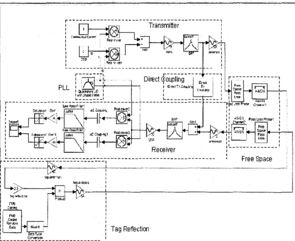
Figure 3 is the simulation environment of return link. The transmitter sends a continuous carrier to power up tag. The free space is modeled by pass loss with phase changing due to distance between reader and tag. A WGN channel is added to model the noise sources from space. Another source of receiving power is the direct coupling from TX to RX. It is modeled by a proper gain and phase delay.
The tag is modeled by coding method, antenna gain, and percent of reflection. The receiver includes band pass filter, LNA, Mixer, AC coupling, channel select filter and the variable gain stages. The BER performance can be seen by comparing the received and down converted signal with the data tag backscattered
~ce
Cocirg
Rai se Ca;i ne HI bert
: ~tlO '
Mf'l O"QQf .._... I
oc
Snttth fi Iter
. - ... .
.
IQ Inml aoce
rH31 s:I3/
ON 9N t ch: ~h:o,---
! -~ . . . .
t:Bta . Processi rg:
. . .
. . ..Figure 2 Transmitter simulation environment in Simulink
Free Space
...
.. -·· - --·-···
' Tag JEfl ecti on
' c~
,..
' •L • • • • .... • • • • • • • .. • ... • .. •
Figure 3 Simulation of return link
3. Models of the Building Blocks of RFID System 3.1 Model ofTransmitter
The architecture of transmitter is chosen to be I/Q-branches for the reasons of SSB transmission and different modulation methods such as ASK or PSK.
The simulation in this paper is based on [3]. The coding for forward link is Manchester coding.
The transmitter should fulfill the protocol and support the DSB or SSB transmitting for forward link, send an un-modulated carrier for return link:. Figure 4 gives the configurations of transmitter for different modulations.
1
0
Figure 4 Configurations for SSB, DSB and return link
3.1.1 Coding
subcarrier coding for return link [3]. The power spectral density of Manchester subcarrier is different with Manchester since a DC component is added by the asymmetric probability of two levels.
BER is introduced to evaluate the performance of a digital communication system. In forward link, the CNR is large enough for a tag to demodulate data by envelope detector. The tag reflects the incident power, and the reflect power is very weak for a passive tag since it can only send the return data through changing RCS (radar cross section) which is very small. If most of the power were reflected, the tag would not work. If less power were reflected, reader would not reach a high sensitivity physically. The SNR requisition under a given BER for some modulation type is listed in Table 1. A BER of le-3 is chosen for RFID system in some products.
Table l. SNR requisition of different modulation types
BER le-3 le-5 le-7
PSK 6.8dB 9.6dB 11.4dB
FMO/Manchester subcarrier 9.8dB 12.6dB 14.4dB
FSK ll.OdB 13.4dB 14.9dB
ASK 12.6dB 15.2dB 18.6dB
3.1.2 Raised Cosine Filer
A band-limited signal, which has no lSI (intersymbol interference), should satisfy Nyquist criterion [4]. Usually, it is realized by a raised cosine filter. Figure 5 is the simulation result of Manchester coding with roll off factor 0.1, 0.5 and 1, the oversampling ratio 32, and data rate 80kbps.
To meet the stringent waveform bound less than 5% of the modulated signal, the roll off factor must chosen to be I.
2
15 '
·I . . . .
-15
• • f •
··~ .: ... , ...
: .
A ;· i J\
alpha=() I - alplla=OS - alpha= I
... ··:· .. i ' 1 .,.
~
i tt ·. ,.. ' .
.. :- ... .
~
...
~-···... , ... 9 .. .
HDJ 1100 1200
v
I:Dl UOO 1!Dl 1600 1700 Tome (us)Figure 5 Manchester coding after raised cosine filter
3.1.3 Hilbert Transform
SSB-AM is derived by removing one of the sidebands of DSB-AM, and occupies one half bandwidth ofDSB-AM [4]. The signal power ofSSB is haJfofthe DSB modulation. The noise power in the bandwidth is also half of the DSB due to the half bandwidth. Therefore, the SNR of SSB and
1 .••
1- ReaiPart
I
_]- Image Pan
1{\
.. os 0
]J · · · · · , ..
~ io
:lO
.{)5 ••
. , . . v ,
~ . . . . ; .... \,.-..J ... : ·;·W
&D liiD 700
lime (us)
Figure 6 Hilbert transform of Manchester coding
When the signals are up-converted and added, the SSB-AM is produced. 1/Q mismatch is one of the problems both in VQ transmitter and in receiver. ln transmitter, the phase and gain mismatch of 1/Q-branches will degrade the suppression of SSB transmission since the DSB transmission only occupies the 1-branch. In practice, it is desirable to maintain the amplitude mismatch below I dB and phase error blow 5° [5].
3.1.4 Quantization
The signal is over sampled by FIR filter such as raised filter and Hilbert transform. After digital signal processing, the digitized signal is send into analog part. In practical, a DAC will convert digital signals into analog, which yields quantization error. The clock of DAC is usually higher than the signal. In an oversampling circuit, the maximum sinusoidal power to the quantization noise is [6]
SNRmax =6.02N+l.76+101og(OSR) (1)
N is number of the quantization bits, OSR is the oversampling rate. The first term of (1) is the SNR due to the N-bit quantizer while the OSR term is the SNR enhancement obtained from oversampling. This can model the noise power induced by the DAC. The low pass filter after DAC is to smooth the waveform and lower the high order harmonics.
3.1.5 Up-converter
The transmitter architecture of Figure 2 suffers from LO pulling [5). The output power of PA is a modulated waveform with high power and a spectrum centered around the LO frequency. Despite of various shielding techniques employed to isolate the VCO, the "noisy" output of the PA still corrupts the oscillator spectrum through "injection pulling" or "injection locking". The problem worsens if the PA is turned on and off periodically to save power. Therefore, the VCO must be followed by a buffer stage with high reverse isolation between the VCO and the PA.
3.1.6 Power Amplifier
The power amplifier is modeled with nonlinearities, IIP2 and IIP3 for different types of power amplifiers. The AM/PM effect of amplifier is not included since tags are not sensitive to the phase of the carrier. The power amplifier is to give a proper power gain and the gain range of the power
3.1.7 Output Band Pass Filer
The output band pass filter is to remove the out of band spurious spectrum. A fourth order Bessel filter is selected with the bandwidth range from 860MHz to 960MHz. The maximum input power of the filter is about t W and it can be implemented by passive elements.
3.2 Model of Tags 3.2.1 Tag Received Power In forward link, the output power is
The Effective Isotropic Radiated Power (EIRP) of the reader is PEIRP· The typical maximum output power is SOOmW, 2W (ERP, CEPT) and 4W (EIRP, FCC). Converted to dBm, the permitted maximum limits are about 29dBm (500mW ERP, 825mW EJRP), 35dBm (2W ERP, 3.3W EIRP) and 36dBm (4W EIRP). GTX is the gain of the transmitter antenna. The typical value is assumed to be 6dBi.
Therefore, the maximum output power from power amplifier should be 23dBm, 29dBm and 30dBm, respectively.
The power transmitted from reader to tag can be expressed as
).. is the wavelength of the carrier. d is the distance from reader to tag.
The tag available power vs. distance can be seen in Figure 7. From the industrial experience, RF input power of lOuW (-20dBm) to SOuW (-13dBm) is required to power on tag.
. . .
2ll o 1 o • • •"' •• o • ... • • ••!•••••• ••••• o . . . o o o oeo
~ 10
I
a...,
..
l!! ~
:: -10
...
-20
·.
-~0~~--~2--~3~-~L-~5--~6---L--~8--~9--~10 Link 01stance (m)
Figure 7 Tag received power before the rectifier
3.2.2 Tag Reflection Model
As we all know, tag received power includes two parts, the reflected power and the available power can be used by the chip. The distribution of these two parts is very critical for a maximum
distance. Ln [7], a detail calculation is performed.
The available power from antenna can be used by the rectifier is
PRJ-,m = piPR/·,m,l + p2PRf.,m,2
The reflect power is
2
= 8
i [P~(1-IPl)+p2 (1-lp2 nJ
ant
~.= .!.Iii -412
Rrod (5)8
(4)
v0 is the peak source voltage that would be observed if the antenna were not loaded by the IC. In time domain, the probabilities that chip in state I and state 2 are pI and p2. P 1.2 are the reflection coefficients. Ram is the real part of the antenna impedance. i1.2 are the current flow through the impedance. Rrad is radiation impedance of antenna.
3.3 Wireless Channel
The wireless channel is modeled by the Friis transmission equation (3). The Palomar project introduced power shadow by reflections of the walls [8].
RFID system is a LOS (Line of Sight) communication system. The influence of reflection by the environment should be considered. The radio propagation model can be expressed as
2 2
( A. ) 112
1 ( . )
112~
( )1 ( . )
P,
= P, - G0 - exp -Jkr0 +G,Llr a,
-exp -Jkr,47Z'
'o
,.1 r, (6)Pr is the received power. P1 is the transmitted power. The antenna gain of transmitter is different in different direction. Go is the antenna gain of the direct path. G1 is the antenna gain of the propagation way numbered i. r (a ,) is the reflection coefficient of each ray. Figure 9 is the simulation results of tag and reader received power due to reflection by walls.
4
!llltanco b_.., Ruder and To11 (m)
(a)
~.~~~~~~0~~~2~~,.~~~&~~1B~~E~n l.ongth oiRoorn (m)
(b)
Figure 8 Simulation of multi-ray indoor propagation model for RFID (a) Tag received power due to reflection by walls,
(b) Reader received power due to reflection by walls
gain since the tag is not facing the center of reader antenna results a smaller power than the Friis model. In this region, power level changes smaller than the far regions. When the distance gets larger, the reflections become more important. When tag is close to the wall that reader faced, the received power by tag changes rapidly and deeply and the maximal amplitude may exceed I OdB. The minimum RF input power for power up the tag would not always get enough because of shadow effect. For a simple analysis and simulation, Friis transmission equation is a good approximation.
Figure 8 (b) is the received reflection power by reader. When the distance between the reader and the wall faced to reader antenna increases, the reflection power changes.
3.3 Model of Receiver 3.3.1 Antenna
The antenna can be configured in two types, two antennas or one antenna with a circulator. In return link, the receiver of reader listens to the response of tag while the transmitter send a continuous wave to power up the tag. It is very critical to have a high isolation between TX and RX for a high perfonnance reader.
The direct coupling from TX to RX with one antenna is larger than two antennas because of low isolation perfonnance of circulator. Assume the transmitting power is 36dBm (FCC), the isolation of a circulator is about 35dB (Commercial circulator can hardly exceed 40dB). Therefore, the power seen in the receiver is about OdBm. Jn this case, the receiver circuit should have a large dynamic range to handle the relative large signal and detect the weak signal backscattered from tag. The direct coupling signal is much larger than the reflection from the environment and the environment can be ignored.
3.3.2 LNA
The LNA is optional for different antenna configurations. If it is configured with two antennas, the isolation is relative high. In this case, LNA is used to get a proper gain and better NF of receiver.
The gain range is from I 0 to I 0 dB. 1 f a circulator is used, the isolation is very poor and the power into the receiver is very large. In this case, a power splitter is used instead of LNA because of its capability of handling large signal.
3.3.3 Direct Conversion
The architecture of receiver is direct conversion receiver suitable for multi-protocol operation.
The DC offsets are very large due to low isolation between the TX and RX. The receiver will have a multi-stage gain to amplifier the weak signal. Since the DC offset is much larger than the signal, the offset may saturate the amplifier if it is not removed. An ac coupling stage is inserted after the mixer filtering out the DC component.
The 1/Q mismatch of the receiver is different with the transmitter. In receiver, the 1/Q mismatch will corrupt the downconverted signal constellation such as QPSK. In RFID system, the modulation used in return link is AM and PSK [8]. It has less influence in the receiver with amplitude modulation.
3.3.4 Filter
A high order channel select filter is applied to get a sufficient out of band suppression. The filter type in the receiver is a 5-order Butterworh filter due to it flatness in the passband and suitable for amplitude modulation.
3.3.5 Base-band DSP
The baseband DSP is to decode the signal from ADC. The DSP should combine the signal power
of UQ branch for maximizing the signal power to get the best BER performance. In additional, some filtering must be made to suppress the out of band interference in further. This part is not included in our simuJation.
4. Simulation Results
4.1 Simulation Results ofTransmitter
The time domain simulation costs a lot of time and we get many data to be processed. Figure 9 is the DSB transmission of Manchester coding with 80k data rate in time domain.
Figure 9 DSB transmission of Manchester coding with 80kbps (a) 100% modulation depth, (b) 30% modulation depth
Figure I 0 is the mask analysis of the transmission corresponding to Figure 9. The x-axis is the frequency offset of the carrier. The red line is the frequency from ETSI EN 302 208-1 (9].
:II
20
l a 10 li 0 ;.
~ e -1o
ln.20 i
Ln
:II
20 If ~ 10
~ ~ 0
e i ·10
en
i
·200.
(a) (b)
Figure 10 Spectrum analysis of DSB transmission (a) 100% modulation depth, (b) 30% modulation depth
Figure II is the SSB transmission of Manchester coding with 80k data rate in time domain.
(a) (b)
Figure It SSB transmission of Manchester coding witb 80kbps (a) tOO% modulation depth, (b) 30% modulation depth
Figure 12 is the mask anaJysis of the transmission corresponding to Figure II. The mask should have some offset since it is transmitting with single sideband .
.co
))
E'lll
! i 10
A 0
~
A-tO
! l l l
·l l
-«1
~
~ • ••!
lD '? 10
~ 0
f
10~-lll
&
.,.:1)
lD
·I 0 I 2 3 4
f~llbl
(a) (b)
Figure 12 Spectrum analysis ofSSB transmission (a) 100% modulation depth, (b) 30% modulation depth
•
l
-
,
I
.
lt
: •
.
' '
'
'
...
!
-«11---'iii----~--+ . ..
.. , .'
~
.
d I
1 .08 .06 .04 .02 0 02 04 06 08 1
fiW'lU-=J(HZ) l1rl
(a) (b)
Figure 13 Tag reflected power
(a) FMO coding with 640kbps, (b) Manchester subcarrier coding with 64kbps
4.2 Simulation Results ofTag
The coding of the return link is FMO and Manchester subcarrier. Figure 13 is the simulation results of tag reflected power at the distance of 2m. Figure 13 (a) is the FMO coding with 640kbps and Figure 13 (b) is the Manchester subcarrier coding with 64kbps.
4.3 Simulation Results of Receiver
Figure 14 is the simulation results of reader-received signals with return link FMO coding 640kbps and 2m-operation distance from reader to tag. The up panel is the received signal of 1-branch and the bottom panel is the received signal ofQ-branch. From the signals shown in Figure 14 (a). we can get the conclusion as follows. At first, the circuits are all in saturated region with the assumption of linear range from I to I. The saturated signal is due to the large DC offset. The saturation time of 1-branch is larger than the Q-branch. The reason is that the direct coupling affects Q-branch more severely than 1-branch results a larger DC offset and a longer settling time. The SNR is better in 1-branch than in Q-branch. Different results can be obtained by changing the phase delay of the direct coupling and the operation distance from reader to tag, Figure 14 (b). The low frequency noise because of LO phase noise and fluctuation of amplitude can hardly removed. Therefore, the circuit of detector is critical.
(a)
Figure 14 Reader received signals (a) Example I, (b) Example 2
(b)
(Up panel is 1-brancb; bottom panel is Q-brancb) 5. Conclusion
In this paper, a system model is developed with some simulation results. At first, the simulation model is introduced briefly. Models of DSP, transmitter and wireless channel, front-end of tag and receiver model are introduced. Finally, some simulation results are presented.
There are some critical problems to be discussed. The raised cosine filter affects the spectrum of the output, and the parameters should be handled carefully. The SSB transmission is not very ideal from the simulation results since a finite length of data is processed. In receiver of reader, the suppression of DC offset and transient response may drive the follow-up circuits into saturation. The
circuits, variable gain stage and detector of receiver are also challenges. The reflection of the objects in environment will mainly affect the operation of tag, and special attention should be paid to diminish the effect of Fresnel zones. All the problems mentioned above should be solved in fur
![Fig 3: Block diagram ofi-Q imbalance on Simulink [I]](https://thumb-ap.123doks.com/thumbv2/azpdforg/11131625.0/14.851.188.760.114.416/fig-block-diagram-ofi-q-imbalance-on-simulink.webp)
