This project involves the study about available wireless systems and how these wireless systems can be implemented in the project. Test method is developed by conducting an experiment in the transfer of the data and the performance measurements are taken into account in the completion of the project. For the RF module, C codes are developed for PIC microcontroller on the transmitter and receiver side.
I also give special thanks to my colleagues who have helped me with valuable advice and opinions regarding the project.
INTRODUCTION
Background of Study
Objective
Scope of Study
THEORY
KC-21 Bluetooth Module
When an RF current is applied to an antenna, an electromagnetic field is created, which is then able to propagate through space. As for this project, the transmission process will use the Amplitude-shift keying (ASK) method. ASK is a form of modulation that represents digital data as differing in the amplitude of a carrier wave [2].
![Figure 1 Bluetooth KC-21 Module [8]](https://thumb-ap.123doks.com/thumbv2/azpdforg/10260270.0/14.829.325.506.87.410/figure-1-bluetooth-kc-21-module-8.webp)
Sfi) -f(t)sin(2jifct + 6)
TLP-434A Transmitter
TTTT
- RLP434A Receiver
- Encoder
- Decoder
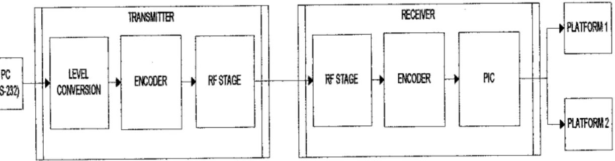
- Serial Communication Interface RS-232
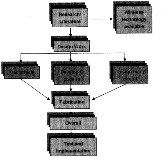
- PROJECT WORK
- Literature review and analysis
- Circuit design and modeling
- Integrating software design with hardware
- Tools required
- RESULT
- Data Transmission for PC to PIC 16F877 Microcontroller
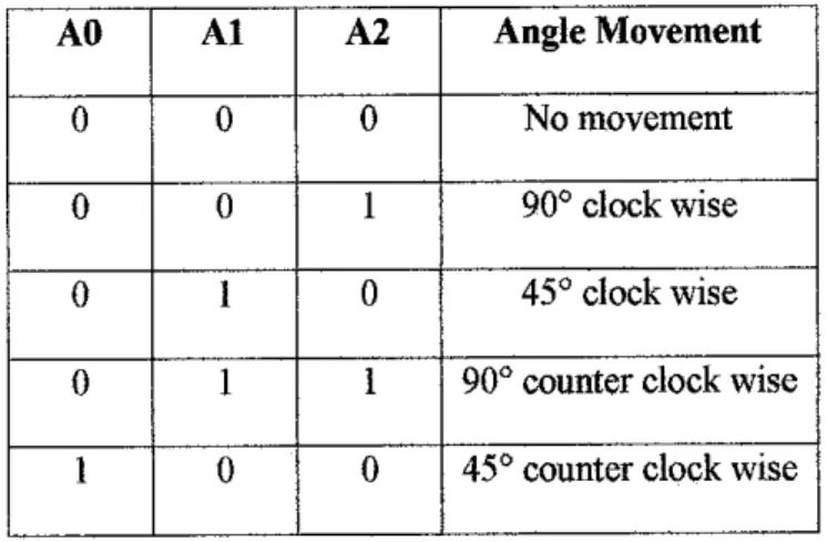
A 2 millisecond pulse train positions the servo motor to the right and a 1.5 millisecond pulse train positions the motor in the 90° position. Two servo motors are attached to the platform to perform the pan and tilt operation. This procedure is used to test how the RS-232 serial communication input is processed and how the input is transferred to the microcontroller by looking at the incoming and outgoing data.
The bit streams representing the character value for the PC will be sent to the microcontroller's communication pin via RS232.
![Figure 5 Encoder 18 pin [5]](https://thumb-ap.123doks.com/thumbv2/azpdforg/10260270.0/17.829.144.702.161.1118/figure-5-encoder-18-pin-5.webp)
CONCLUSION AND RECOMMENDATION
APPENDICES
APPENDIX A
BLUETOOTH KC-21 DATASHEET
Features Fully embedded Bluetooth v1.2 Serial Profile Class2radio Complete RF ready module Wireless data communications ARM7 microprocessor up to 48MHz 8Mb flash memory 921Kbaud data throughput Built-in chip antenna 128-bit encrypted security Range up to 20m LOS SPI interface, up to 24MHz 14 general purpose I /O ATcommandset Multipoint Capability FCC & Bluetooth Qualified Additional Documentation • Getting Started Guide kcSerial2.2UfeerGuide • kcSerial2.2ReferenceGuide • kcSerial 2.2 Configuration Guide KC-21DatasheetBluetoothOEMModule ©Bluetooth' 15mmx27mm Description One of the most powerful Bluetooth modules available, the KC-2 1 Bluetooth OEM module is designed to maximum flexibility. The KC-21 module includes 14 general-purpose input/output lines and offers high-speed serial communication up to 921Kbaud. The KC-21 is a surface mount PCB module that provides fully integrated Bluetooth wireless technology ready to use.
Hardware Specifications General Conditions (Vdo= 3.3V and 25°C) Recommended Operating Conditions RatingMinTypicalMaxUnit Operating Temperature Range-25-80°C SupplyVottageVoD2.73.33.6Voits SignalPinVoltage-3.3-Volts2.Maximum MaxUnit StorageTemperature Range-40-+150° C Supply Voltage,VDD- 0.3-+3.6Volts RF Input Power---5dBm Current Consumption ModesAvgUnit ACLdata115KBaudUARTatmaxthroughput(Master)35.0mA ACLdata115KBaudUARTatmaxthroughput(SlaveA traffic05.0mA traffic)1.0mA traffic05.0mA traffic. traffic,slave28.0mA Connectioninsniff(TsniffMQOms), nodatatraffic,master10.2mA Connectioninsniff(Tsniff=10Qms),nodatatraffic,stave10.8mA Connectioninsniff(Tsniff=375ms),nodatatraffic,master2.75mA Connectioninsniff(Tsniff=376ms),nodatatraffic,withAstandby3. 50mdeepsle,withAbystandby3.50mdeepsle . 16mA Page/Query Scan, Deep Sleep 2.1mA Peak Current 90mA. FCC Regulatory Compliance This module has been tested and found to comply with the FCC Part 5 Rules. Operation is subject to the following two conditions: (1) This device may not cause harmful interference, and (2) this device must accept any interference received, including interference that may cause undesired operation.
Limited Modular Transmitter Approval is given instead of Modular Transmitter Approval because the following condition is not met: • The module has no RF shielding. In accordance with FCC document, DA 00-1407, all final use of this device by OEMs must, (1) be approved by the module manufacturer, KC Wirefree, (2) final installation must follow the instructions in this user manual, (3 ) a written agreement with the OEM will specify which products are approved for this module's final installation to control its end use and ensure FCC Part 15 compliance. FCCLabelInstructions The exterior of end products containing a KC-21 unit must display a label referring to the module provided.
Normally KC Wirefree supplies devices with the final firmware already pre-loaded, so this should not be part of the normal production of a product. Run the BurnFirmWare_pX.bat file, where X represents the COM port, 1-4, of the PC connection.
TfJvufyee
APPENDIX B
TLP-434A/RLP-434A DATASHEET
TLP434A Ultra Small Transmitter Pin 1: GND Pin2: Data Pin 3: Vcc Pin 4: Antenna (RF output) Frequency 315,418 and 433.92 Mhz Modulation:ASK Operating Voltage: 2-12 VDC SymbolParameterConditiontpMeasuresVolimxMinTy.
APPENDIX C
HT-12E ENCODER DATASHEET
HOLTEK
2n Series of Encoders
Input Pins for Address/Data AD8-AD11 Setting These pins can be externally set to VSS or left open.
The 212 series encoders begin a four-word transmission cycle upon receipt of a transmission enable (TE for the HT12E or D8-D11 for the HT12A, active low). This cycle repeats as long as the transmission enable (TE or D8-D11) is held low. Once the transmission enable is high again, the encoder output completes its last cycle and then stops, as shown below.
When the transmission enable is removed during a transmission, the DOUT pin outputs a full word and then stops. When the transmission enable is removed during a transmission, the DOUT outputs a full word and then adds 7 words, all with the data code. The HT12A's address/data bits are transmitted using a 38 kHz carrier for infrared remote control flexibility.
If the transmit enable signal is applied, the encoder scans and transmits the status of the 12 address/data bits serially in the order AO to ADll for the HT12E encoder and AO to Dll for the HT12A. The following is the address/data sequence table for the various models of the 21" encoder series. For the HT12E encoders, transmission is enabled by applying a low signal to the TE pin.
For HT12A encoders, transmission is enabled by applying a low signal to one of the data pins D8-D11. The HT12E must closely follow the application circuits provided by Holtek (see "Apphcation Circuits cuits").
APPENDIX D
HT-12D DECODER DATASHEET
They are paired with Holtek's Encoder Series 2 (see Encoder/Decoder Cross Reference Table). Decoders receive serial addresses and data from a programmed series of 2 encoders that are transmitted by the carrier using an RF or IR transmission medium.
2 if2 Series of Decoders
212 Series of Decoders
Stresses exceeding the range specified in the "Absolute Maxi Mum Ratings" can cause significant damage to the device. Functional operation of this device under conditions other than those listed in the specification is not implied, and prolonged exposure to extreme conditions may affect the reliability of the device. The 212 series of decoders offer different combinations of address and data pins in different packages in order to pair with the 2 series of.
The decoders receive data sent by an encoder and interpret the first N bits of the code period as addresses and the last 12 N bits as data, where N is the address code number. A signal on the DIN pin activates the oscillator which in turn decodes the incoming address and data. If the received address codes all match the contents of the decoder's local address, the 12-N data bits are decoded to activate the output pins and the VT pin is set high to indicate a valid transmission.
The HT12D, on the other hand, provides 4 latch-type data pins whose data remains unchanged until new data is received. The oscillator is disabled in standby mode and is activated when a logic "high" signal is applied to the DIN pin. This means that DIN must be low when there is no input signal.
A correct device must be selected according to the requirements of the individual addresses and data.
APPENDIX E MAX232 DATASHEET
MAX232, MAX232I DUAL EIA-232 DRIVERS/RECEIVERS
UAX232, MAX232I
DUAL EIA-232 DRIVERS/RECEIVERS
MAX232, MAX232I
U1AX232, MAX232I
Texas Instruments Incorporated and its subsidiaries (Tl) reserve the right to make corrections, modifications, improvements and other changes to its products and services at any time and to discontinue products or services without notice. Customers must obtain the latest relevant information before placing orders and must verify that such information is current and complete. All products are sold under Tl's terms and conditions of sale, which are provided at the confirmation of the order.
Tl warrants the performance of its hardware products to the specifications applicable at the time of sale in accordance with Tl's standard warranty. Testing and other quality control techniques are used to the extent Tl deems necessary to support this warranty. Except when required by government requirements, testing of all parameters of each product is not necessarily performed.
To minimize the risks associated with customer products and applications, customers must provide adequate design and operational safeguards. Tl does not warrant or represent that any license, express or implied, is granted under any Tl patent, copyright, mask work right, or other intellectual property right of Tl with respect to any combination, machine, or process in which Tl products or services are used. used. Information published by Tl regarding third party products or services does not constitute a license by Tl to use such products or services, nor a warranty or endorsement thereof.
Use of such information may require a license from a third party under the patents or other intellectual property of a third party, or a license from Tl under the patents or other intellectual property of Tl. The resale of Tl products or services with representations that differ from or exceed the parameters Tl states for that product or service voids all express and implied warranties for the related Tl product or service and.
APPENDIX F
PIC16F84 DATASHEET
PIC16F84A
Data Memory Organization
The first is the Special Function Registers (SFR) area, while the second is the General Purpose Registers (GPR) area. The entire data memory can be accessed directly via the absolute address of each register file or indirectly via the File Select Register (FSR) (Section 2.5). The data memory is divided into two banks containing the general purpose registers and the special function registers.
Each General Purpose Register (GPR) is 8 bits wide and can be accessed directly or indirectly through the FSR (Section 2.5).
Special Function Registers
APPENDIX G
PIC16F877 DATASHEET
Timerl: 16-bit timer/counter with prescaier, can be incremented during sleep via external crystal/clock. Programmable input multiplexing from device inputs and internal voltage reference - Comparator outputs are externally accessible.
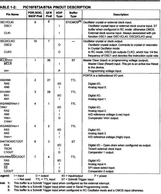
PIC16F87XA
This buffer is a Schmitt Trigger input when This buffer is a Schmitt Trigger input when This buffer is a Schmitt Trigger input when. In RC mode, the OSC2 pin outputs CLKO, which has 1/4 the frequency of OSC1 and indicates the instruction cycle rate. This buffer is a Schmitt Trigger input when configured in RC Oscillator mode and a CMOS input otherwise.
No TTL used = TTL Input This buffer is a Schmitt Trigger input This buffer is a SchmittTrigger input This buffer is a SchmittTrigger input.
APPENDIX H
SERVO MOTOR CIRCUIT
CIRCUIT FOR CONNECTING PC TO MICROCONTROLLER
APPENDIX J
TRANSMITTER CIRCUIT
APPENDIX K RECEIVER CIRCUIT
APPENDIX L
BLUETOOTH CIRCUIT CONNECTION
APPENDIX M
CODING FOR TESTING SERVO MOVEMENT
APPENDIX N
CODING FOR DATA TRANSMISSION FROM PC TO PIC
APPENDIX O
CODING FOR TRANSMITTER
Setthsb(OxOO); //set port B as outputport
Output_high(PIN_B4);
APPENDIX P
CODING FOR RECEIVER
Data=0;
Data^inputjy;
APPENDIX Q
CODING FOR TESTING OF BLUETOOTH DATA TRANSMISSION
BRGHM;
TXEN=1;
CREN-1;
SPEN=1;
APPENDIX R
CODING FOR WIRELESS PANT AND TILT SURVEILLANCE PLATFORM (BLUETOOTH)
BRGHN1;
TXEN-1;
APPENDIX S
CODING FOR WIRELESS PANT AND TILT SURVEILLANCE PLATFORM (SERVO)
![Table 1 KC-21 Pin Configuration [8]](https://thumb-ap.123doks.com/thumbv2/azpdforg/10260270.0/14.829.97.741.594.985/table-1-kc-21-pin-configuration-8.webp)
![Figure 2 Amplitude-shift keying [3]](https://thumb-ap.123doks.com/thumbv2/azpdforg/10260270.0/15.829.182.656.516.764/figure-2-amplitude-shift-keying-3.webp)
![Figure 6 Flow chart of the encoder [5]](https://thumb-ap.123doks.com/thumbv2/azpdforg/10260270.0/17.829.169.644.544.1047/figure-6-flow-chart-of-the-encoder-5.webp)