i
SMART ELECTRONIC LIGHTING BALLAST APPLICATION FOR SALTWATER ENVIRONMENT
By
ROHANA BT MOHD LUDIN
FINAL PROJECT REPORT
Submitted to the Department of Electrical & Electronic Engineering in Partial Fulfillment of the Requirements
for the Degree
Bachelor of Engineering (Hons) (Electrical & Electronic Engineering)
Universiti Teknologi PETRONAS Bandar Seri Iskandar
31750 Tronoh Perak Darul Ridzuan
Copyright 2012 by
Rohana Bt Mohd Ludin, 2012
ii
CERTIFICATION OF APPROVAL
SMART ELECTRONIC LIGHTING BALLAST APPLICATION FOR SALTWATER ENVIRONMENT
by
Rohana Bt Mohd Ludin
A project dissertation submitted to the Department of Electrical & Electronic Engineering
Universiti Teknologi PETRONAS in partial fulfilment of the requirement for the
Bachelor of Engineering (Hons) (Electrical & Electronic Engineering)
Approved:
__________________________
(Dr. Nor Zaihar bin Yahaya) Project Supervisor
UNIVERSITI TEKNOLOGI PETRONAS TRONOH, PERAK
September 2012
iii
CERTIFICATION OF ORIGINALITY
This is to certify that I am responsible for the work submitted in this project, that the original work is my own except as specified in the references and acknowledgements, and that the original work contained herein have not been undertaken or done by unspecified sources or persons.
__________________________
Rohana Bt Mohd Ludin
iv
ACKNOWLEDGMENT
I take this opportunity to express my profound gratitude and deep regards to my supervisor Dr Nor Zaihar B Yahaya for his exemplary guidance, monitoring and constant encouragement throughout the course of this thesis. The blessing, help and guidance given by him time to time shall carry me a long way in the journey of life on which I am about to embark.
I am obliged to technician for the valuable information provided by them in their respective fields. I am grateful for their cooperation during the period of my project.
Lastly, I thank almighty, my parents, brother, sisters and friends for their constant encouragement without which this thesis would not be possible.
v
ABSTRACT
This work is about the design methodology of electronic ballast for saltwater environment application. The effect of environment to electronic devices research stated that electronic circuit exposed to salty environment has high tendency to damage. Therefore, the protection scheme needs to be added to avoid malfunction.
The power supply cut-off circuit is the simplest way to protect ballast from damage at the input terminal. All the circuit simulation is performed using NI Multisim circuit simulator. It is found that self oscillating electronic ballast with power supply cut off circuit is the simplest way to protect ballast circuit at saltwater application. By stages, an electronic ballast circuit is simulated and the output waveform is observed.
Start with bridge rectifier, which is produce smooth DC voltage. Then follow by basic ballast circuit. Next, the circuit improved using self oscillating driver. Lastly, electronic ballast circuit combined with power supply circuit.
vi
TABLE OF CONTENTS
Page
ABSTRACT………..….v
LIST OF FIGURES………..…viii
LIST OF TABLES……….x
CHAPTER 1 INTRODUCTION………1
1.1 Introduction to Electronic Ballast………..1
1.2 Background Studies………2
1.3 Problem Statement ………4
1.4 Project Objectives………..5
1.5 Feasibility Study………5
1.6 Contribution & Significant Of Study……….5
1.7 Gantt Chart……….6
CHAPTER 2 LITERATURE REVIEW...7
2.1 Lighting Ballast….……….7
2.1.1 Magnetic Ballast………...7
2.1.2 Advantages and Disadvantages of Magnetic Ballast……..10
2.1.3 Electronic Ballast………....11
2.1.4 Advantages and Disadvantages of Electronic Ballast…....12
2.1.5 Electronic Ballast circuit and operating principle……...13
2.1.5.1 Full Bridge Rectifier………...…………...14
2.1.5.2 Series LC Resonance Circuit………...15
2.2 Saltwater Environment Application……….…....16
2.2.1 The effect of saltwater environment on electronic ballast..18
2.3 Reviews on Electronic Ballast Design………...20
2.3.1 Review on short circuit protection...21
2.4 Electronic Ballast Efficiency………..…..….23
CHAPTER 3 RESEARCH METHODOLOGY………...24
3.0 Procedure Identification………..…..24
3.1 Research on Electronic Ballast………..………25
3.2 Research on Impact of Saltwater Environment to Electronic Ballast...26
3.3 Design Approach………..….27
vii
3.3.1 Required software………..27
3.3.2 Fluorescent lamp Specification………..28
3.3.3 Electronic Ballast Approach Circuit Diagram…….….….29
3.3.4 Improved Electronic Ballast circuit……….…..33
3.3.5 Cut off circuit………....39
3.3.6 NI Multisim Simulation………...42
3.4 Performance Analysis……….42
CHAPTER 4 RESULT AND DISCUSSION...43
4.1 Electronic Ballast Circuit and Operating Principle……….43
4.1.1 Full Bridge Rectifier………..43
4.2 The Effect of Saltwater Environment on Electronic Ballast…..46
4.3 Electronic Circuit Ballast Simulation………...48
4.3.1 Bridge Rectifier Simulation………..49
4.3.1.1 Bode plot of LC Series Resonant Circuit...49
4.3.1.2 Self oscillating driver...51
4.3.2 Cut off Simulation ………....52
CHAPTER 5 CONCLUSION...54
REFERENCES……….…….55
Appendix A...60
viii
LIST OF FIGURES Page
FIGURE 1 Compact fluorescent lamp and linear fluorescent lamp………..1
FIGURE 2 Damaged Electronic Ballast Used By Petronas Carigali,Miri…………2
FIGURE 3 Basic electronic ballast flow diagram………..3
FIGURE 4 Short circuit in microelectronic due to corrosion[6]………4
FIGURE 5 Magnetic ballast used in older lighting [7]………..7
FIGURE 6 Schematic of traditional ballast with series of capacitor [8]……...….8
FIGURE 7 Voltage and current waveform...9
FIGURE 8 Electronic Ballast used solid state electronic circuitry [13]…………...11
FIGURE 9 Electronic ballast circuitry [13]...………...…………11
FIGURE 10 Block diagram of an electronic ballast...13
FIGURE 11 Full Bridge Rectifier [14]...14
FIGURE 12 Series LC network ………..….…...15
FIGURE 13 Inside magnetic ballast[18]………..……….16
FIGURE 14 Electronic ballast of compact fluorescent lamp [18]…………..……...17
FIGURE 15 Sand inside the ballast casing……….………….…..19
FIGURE 16 Line ground fault...21
FIGURE 17 Short circuit fault...22
FIGURE 18 Flow chart of electronic ballast construction………....24
FIGURE 19 The website of IEEE……….……..………..….…25
FIGURE 20 Sample of Matco Services Inc website………..………...….26
FIGURE 21 NI Multisim software view.………...27
FIGURE 22 Sample of T8 fluorescent lamp……….……….…...28
FIGURE 23 Circuit Configuration [27]………....29
FIGURE 24 Expected input and output waveform of bridge rectifier [28]...30
FIGURE 25 Expected supply current and voltage [27]..………..31
FIGURE 26 Expected simulation result of lamp voltage during starting [27]…....32
FIGURE 27 Expected simulation result for the lamp voltage and current………..32
FIGURE 28 Proposed of self oscillating electronic ballast[30]...33
FIGURE 29 Gate source voltage waveform of one Mosfet [30]...36
FIGURE 30 Current waveform of RLC series filter [30]...36
FIGURE 31 Current and voltage on LCC output filter [30]...37
ix
FIGURE 32 Current and voltage of fluorescent lamp [30]...37
FIGURE 33 Mosfet voltage and current waveforms [30]...38
FIGURE 34 Voltage and current waveform during start up [30]...38
FIGURE 35 Short circuit breaker circuit...39
FIGURE 36 Output voltage of full wave bridge rectifier………...…....43
FIGURE 37 Smooth DC voltage with CB=100μF...44
FIGURE 38 Simulation result for supply voltage L=30 mH ………..…...46
FIGURE 39 Simulation result for supply current L=30 mH ………...46
FIGURE 40 Simulation result for supply voltage L=180mH ………....47
FIGURE 41 Simulation result for supply current L=180mH...47
FIGURE 42 Power supply cut-off circuit...48
FIGURE 43 Self oscillating electronic ballast circuit...48
FIGURE 44 LC series configuration...49
FIGURE 45 Bode plot of LC Series Circuit...49
FIGURE 46 Simulated voltage waveform of gate-source MOSFET (10V/div, 20ms/div)……….51
FIGURE 47 Voltage and current waveform of the lamp...52
FIGURE 48 Output voltage of power supply cut-off circuit without connecting...53 to electronic ballast
x
LIST OF TABLES
Page
TABLE 1 Project Gantt chart………..…6
TABLE 2 Summary of advantages and disadvantages magnetic ballast………..….10
TABLE 3 Summary of Advantages and Disadvantages Electronic Ballast………..12
TABLE 4 Summary of environmental effect to electronic devices ……….…18
TABLE 5 Review on existing electronic ballast design……….………...20
TABLE 6 Design specifications of electronic ballast...35
TABLE 7 Design specification of short circuit protection...41
1
CHAPTER 1 INTRODUCTION
There will be a brief introduction of electronic ballast which is related to the project. Presently, electronic ballast for fluorescent lamp has become common as the standard ballast in the industry. In addition, the technology has also been developed rapidly to increase the performances.
1.1 Introduction To Electronic Ballast
Since the invention of fluorescent lamp in mid 1940, it has been widely used as a preferred real light source due to its high efficiency and longer life span [1]. A fluorescent lamp or fluorescent tube is a gas-discharged lamp that uses electricity to excite mercury vapor as shown in Figure 1. It shows the various type of fluorescent lamp with different size and type.
Figure 1: Compact fluorescent lamp and linear fluorescent lamp [2]
Then, the excited mercury atom produces short-wave ultraviolet light that will cause a phosphor to fluorescent and produce visible light. In order to perform this operation, the fluorescent lamp needs a device called ballast. The main purpose is to generate light of the low pressure flourescent lamp. There are 2 basic types of ballast;
magnetic and electronic [3].
2 1.2 Background Studies
Eletronic ballast is most suitable in saltwater environment than magnetic ballast. The critical environment gives an impact to the performance of the electronic devices such as short circuit. This project is to improve performance of the existing electronic ballast at the saltwater environment. Electronic ballast is widely used for lighting at offshore because electromagnetic ballast is not reliable. This place has high exposure to the salty environment. This environment also effects the electrical contacts, electronic components such as integrated circuit, pcb and the connectors.
Based on Figure 2, the ballast is burnt at the input terminal.
Figure 2 : Damaged electronic ballast which is used in salty environment (offshore) at Petronas Carigali, Miri, Sarawak
Figure 2 shows damaged electronic ballast taken from PETRONAS Carigali, Miri, Sarawak. This project is based on collaboration between PETRONAS Carigali Miri and UTP to investigate the causes of the problem. Figure 3 shows the basic electronic ballast flow diagram. It varies depending on the ballast technology.
3
Figure 3: Basic electronic ballast flow diagram
Main power supply is AC voltage 240V.The function of AC/DC rectifier is to convert AC voltage to DC voltage. It uses bridge rectifier that is made of four diodes in a bridge arrangement to achieve full-wave rectification [4]. The DC/AC inverter is a half-bridge series-resonant parallel-loaded converter.
AC/DC RECTIFIER
DC/AC RECTIFIER
LAMP LIGHT UP MAIN SUPPLY
4 1.3 Problem Statement
Nowadays, electronic ballast is used in environment such as salty, pollution and chemical exposure environment. In this project, the electronic ballast design focuses on the salty environment. Seawater is one of the most influential factors that leads to the corrosion [5]. The most common materials that are attacked by this liquid are metals and alloy.
It does not only affect directly by this liquid but also its surrounding environment. Electrical contacts, microelectronic circuits, and connectors found in common electronics are extremely sensitive to corrosive atmospheric exposure and surface contamination associated with corrosion attack [6] . The presence of less than 1 microgram of corrosion product on the surface of a connector in some cases is sufficient to interrupt the flow of electrons between contacts, thus render the component useless [6].
One of the examples of damaged electronic circuit board is shown in Figure 4. The small corrosion effect will give an effect to the electronic circuit reliability.
This project will investigate the cause and effect of the saltwater environment that cause the damage to electronic ballast.
Figure 4: Short circuit in microelectronic due to corrosion [6]
5 1.4 Project Objectives
1. To understand electronic lighting ballast system
2. To investigate the defect and root cause of the application electronic ballast in saltwater environment
3. To design ballast with cut off power supply protection scheme 4. To analyze the efficiency of the design
1.5 Feasibility Study
This project is to identify the defects and the root cause of the damaged ballast in saltwater environment, where, improvement on existing electronic ballast has become priority. The improvements are to upgrade the protection scheme and analyze the efficiency of the design. This project is feasible within scope and time frame. Table 1 shows the gantt chart of the project. The planning of the project is within the scope of time.
1.6 Contribution & Significance Of Study
The study of electronic ballast used in saltwater environment is basically to find the root cause of the damage. It is also aimed to improve the design to withstand critical environment. This study will give benefit to the ballast company from the research perspective. In addition it will help the company to improve their product efficiency and sale.
Besides, this study will also benefit the clients or customers. They can use this project data as a reference to evaluate electronic ballast they use currently. There are lots of electronic ballasts in the market with different performance and reliability.
6 1.7 Gantt Chart
Table 1: Project Gantt chart
ID Task Name Start Finish Duration Oct 2012 Nov 2012 Dec 2012
16/9 23/9 30/9 7/10 14/10 21/10 28/10 4/11 11/11 18/11 25/11 2/12 9/12 16/12 23/12
1 Discussion on Progress Report 17/9/2012 28/9/2012 10d
27d 5/11/2012
28/9/2012 Working On Progress Report
2 Basic ballast circuit research 24/9/2012 28/9/2012 5d
3 Construct And Simulate In Pspice 28/9/2012 2/11/2012 26d
6 Improve basic circuit 5/11/2012 16/11/2012 10d
7 Preparation On Pre Edx 19/11/2012 23/11/2012 5d
8 Pre-Edx Presentation 26/11/2012 30/11/2012 5d
5d 7/12/2012
3/12/2012 Prepare Draft Report
9 Finalize circuit 26/11/2012 7/12/2012 10d
11 Draft Report Submission 10/12/2012 10/12/2012 1d
15 Viva/Final Presentation 24/12/2012 28/12/2012 5d
10 5 4
1d 5/11/2012
5/11/2012 Progress Report Submission
12 Final & Technical Report Preparation 10/12/2012 17/12/2012 6d 13 Final & Technical Report Submission 17/12/2012 17/12/2012 1d 14 Final Presentation Preparation 17/12/2012 21/12/2012 5d
Table 1 shows the project gantt chart. Project gantt chart is the planning for the whole semester for final year project II.
7
CHAPTER 2
LITERATURE REVIEW
The purpose of literature is to summarize the ideas found with respect to the project. The existing work willbe discussed in this section.
2.1 Lighting Ballast
This section explains the literature review of first objective which is to understand electronic ballast system. There are 2 main types of lighting ballast:
magnetic and electronic. This ballast has their own advantages and disadvantages depending on the application. In this study, electronic ballast is the main focus.
Magnetic ballast will be compared with electronic ballast in terms of lighting operation such as start up time, reliability and flicker.
2.1.1 Magnetic Ballast
First type of ballast is magnetic ballast. Magnetic lamp ballast is effectively a large inductor. It consists of a magnetic core with a copper winding [7].
Figure 5 : Magnetic ballast used in older lighting [7]
8
Figure 6 : Schematic of traditional ballast in series with inductor and capacitor [8]
Figure 5 shows magnetic ballast which is widely used in older lighting system and Figure 6 shows the schematic of conventional ballast in series with inductor and capacitor. For today’s magnetic ballast, the components have been improved in order to excite efficiency and remain the simplicity of the circuit. There are several components of magnetic ballast, such as inductance and capacitor.
Inductance helps control the amount of energy reaching the fluorescent tube.
From Figure 6, when the voltage supply connects to the input of the transformer, current passes through the coils. This creates a magnetic field. It is shown by the arrow mark as I. This phenomenon is called inductance. The inductor can store energy in this magnetic field. But for inductor, this would produce inefficiency.
I
9
Figure 7: Voltage and current waveform
This is because the current is out of phase with the voltage and lags voltage as shown in Figure 7. This will result a poor power factor, meaning power output is less than power input. A capacitor helps improve the power factor and resulting current leads voltage [9].
10
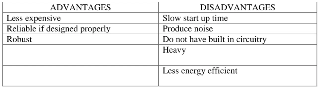
2.1.2 Advantages And Disadvantages Of Magnetic Ballast
Magnetic ballasts are still used because of their affordability. While price range depends on the qualities of the ballast, they are less expensive and easier to produce. The magnetic ballasts are also relatively reliable when designed properly.
Lastly, ballast construction is usually robust. The noticeable disadvantage of magnetic ballast is the start-up time for magnetic ballast to reach full power can be up to 20 minutes [10]. Magnetic ballasts produce a constant hum. But noise output of a magnetic ballasts does not have any effect on performance, it is just distracting.
Magnetic ballasts do not have built in cut off circuitry feature [10]. It means if a magnetic ballast has a short circuit it will continue to operate, but it may give off sparks which may, it turn, cause a fire. Another disadvantage is the weight of magnetic ballast which is heavier than electronic ballast. Magnetic ballasts are less energy efficient, where they dissipate more heat and more exposed fire hazard. Many of them operate for frequency of 60-hertz cycle, which is enough to keep the bulb lit but produce flicker as the frequency tries to maintain constant light. Magnetic ballast do not have the capabilities in dimming and cannot be used with multiple bulbs [11].
The advantages and disadvantages of magnetic ballast are given in Table 2.
Table 2 : Summary of advantages and disadvantes magnetic ballast
ADVANTAGES DISADVANTAGES
Less expensive Slow start up time
Reliable if designed properly Produce noise
Robust Do not have built in circuitry
Heavy
Less energy efficient
11 2.1.3 Electronic Ballast
Electronic ballasts have been available since at least the beginning of the 1980's [12]. The invention of electronic ballast leads to energy consumption reduction and improved performance. Figure 8 shows a sample of electronic ballast in the market.
Figure 8 : Electronic Ballast uses solid state electronic circuitry [13]
Figure 9 : Electronic ballast circuitry [13]
On the other hand, Figure 9 shows the circuit inside casing. They consist of a electronic components such as diode, resistor, capacitor and inductor.
There are few main function of the electronic ballast :
Provide start up voltage across the end electrodes of lamp
Maintain the constant current when the lamp is operating at steady state condition
Ensure the circuit remain stable even under the fault condition
Nowadays, electronic ballast design have been developed to increase the benefits such as robust, energy saving, cost saving, long life span and also efficient.
The feature of the electronic ballast can be added from the aspect of circuit function and also the physical condition to meet requirement at different type of environment.
12
2.1.4 Advantages And Disadvantages Of Electronic Ballast
The start-up time to reach full power for electronic ballast is typically faster than magnetic ballast. Also, electronic ballasts are almost completely silent during its function. Electronic ballast also has lighter weight than magnetic ballast. In addition electronic ballasts are more energy efficient, which means they dissipate less heat.
Less heat output means they are less fire hazard.
It much lighter than magnetic ballast. Electronic ballast is more efficient than magnetic ballast and can save energy. It tends to eliminate flickers and makes the bulb light up more efficient. A very important benefit of electronic ballast is that of cut-off circuitry. They are wired so that if a short circuit is detected, the ballasts cause the light to shut off. So, it can prevent sparks and fire.
Electronic ballast also have some disadvantages. Electronic ballasts cost are more expensive than magnetic ballast. Electronic ballasts are less robustly constructed than magnetic ballast, making them prone to physical and electrical damage. Lastly, the high frequency operation is a potential source of radio interference. Table 3 shows the summarization of the advantages and disadvantages of electronic ballast.
Table 3: Summary of Advantages and Disadvantages Electronic Ballast
ADVANTAGES DISADVANTAGES
Fast start up time Expensive
Not produce noise Less robust
Lighter weight Potential source of radio interference Energy efficient
Cut off circuitry
13
2.1.5 Electronic Ballast circuit and operating principle
Electronic ballast circuit is combination of bridge rectifier and resonant circuit. By definition, it is a device that maintains the current through a fluorescent lamp at the desired constant value and sometimes provides the necessary starting voltage and current. Fluorescent lamp can still function properly without ballast but it will not last long and shorten the lifetime period. A block diagram of high frequency electronic ballast for driving a fluorescent lamp is shown in Figure 10.
Figure 10: Block diagram of an electronic ballast
A power factor correction and low pass filter are usually required in front of the electronic ballast to shape the input line current and to reduce harmonic currents.
The bridge rectifier is required to provide a smooth dc link voltage for the high frequency inverter stage.
14 2.1.5.1 Full Bridge Rectifier
Figure 11 : Full Bridge Rectifier [14]
Figure 11 shows a bridge rectifier uses four diodes in a bridge arrangement to achieve full-wave rectification. It is used to convert AC power to DC power.
Bridge rectifier conducts both current directions, positive and also negative. During positive half-cycle, the top the ac voltage Vac is positive and the bottom is negative.
Therefore, D3 and D2 are in forward biased.
The electrons flow from D3 then continue to D2 and from there to the top of Vac. This will produce a complete closed circuit and current can indeed flow. At this time, D1 & D2 is reversed biased. During negative cycle, the top end of Vac is negative and the bottom is positive. Therefore, D1 and D4 is in forward biased. The electrons flows from D1 through D4. At this time, D3 and D2 is in reversed biased.
D1 D2
D3 D4
Vac
15 2.1.5.2 Series LC Resonance Circuit
Resonance is an RLC circuit in which the capacitive and inductive reactance are equal in magnitude, thereby resulting in purely impedance. Figure 12 shows the configuration of series LC resonance circuit. The circuit consists of resistor, capacitor and inductance. The resonant filter is fundamental in the design of the electronic ballast, because it allows manipulating the frequency spectrum of waveform according to require frequency [15].
A resonant behavior of the circuit is used to preheat, ignite and dim lamp [16]. During preheating, the lamp does not conduct and the circuit is a high Q factor series LC. Q factor is the ratio of reactance to the resistance [17]. Decreasing the frequency will produce high voltage on lamp. At the ignition point, the voltage meets a peak and Q factor changes resulting in low voltage. Decreasing the frequency will increase the voltage until lamp fully light.
Figure 12: Series LC network
16 2.2 Saltwater Environment Application
Next, for second objective is to summarize application of electronic ballast in saltwater application. Seawater is one of the most corroded and most abundant naturally occurring electrolyte, covering about 70 % of the earth's surface [5-17]. The magnetic ballast is not reliable in saltwater application. Due to the disadvantages of magnetic ballast, it is not reliable in saltwater environment.
In this environment, the exposure to short circuit is high because of corrosion or water splash. It means if a magnetic ballast has a short circuit it will continue to operate, but it may give off sparks which may, it turn, cause a fire. Unlike electronic ballast, it has built in cut-off circuitry. So, if there a short circuit is detected, the ballasts cause the light to shut off.
Since magnetic ballast has a lot of disadvantages over electronic ballast, therefore electronic ballast is more efficient in saltwater environment. Magnetic ballast has also high potential to rust because of copper material. Figure 13 shows the constructions inside the magnetic ballast. Almost all of the constructions of magnetic ballast are made from metal.
Figure 13: Inside magnetic ballast [18]
17
Unlike magnetic ballast, electronic ballast uses electronic component and less use of components that made from copper or metal. But, it still has few copper material such as the printed circuit board (PCB). Figure 14 shows inside of electronic ballast which is used for compact fluorescent lamp. The main components in electronic ballast are transformer, capacitor, transistor and resistor.
Figure 14: Electronic ballast of compact fluorescent lamp [18]
18
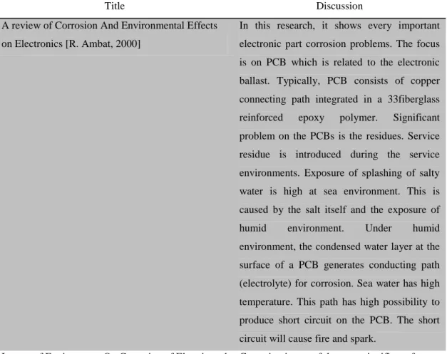
2.2.1 The effect of saltwater environment on electronic ballast
This section will discuss on the effect of saltwater environment on electronic circuit. Table 4 shows the summary of environmental effect to electronic devices.
Table 4: Summary of environmental effect to electronic devices
Title Discussion
A review of Corrosion And Environmental Effects on Electronics [R. Ambat, 2000]
In this research, it shows every important electronic part corrosion problems. The focus is on PCB which is related to the electronic ballast. Typically, PCB consists of copper connecting path integrated in a 33fiberglass reinforced epoxy polymer. Significant problem on the PCBs is the residues. Service residue is introduced during the service environments. Exposure of splashing of salty water is high at sea environment. This is caused by the salt itself and the exposure of humid environment. Under humid environment, the condensed water layer at the surface of a PCB generates conducting path (electrolyte) for corrosion. Sea water has high temperature. This path has high possibility to produce short circuit on the PCB. The short circuit will cause fire and spark.
Impact of Environment On Corrosion of Electric and Electronic Devices [E. Z. Delgadp, 1994]
Corrosion is one of the most significant factors affecting the reliability of electrical and electronic equipment. The failure of the electronic device is due to contaminants of environment, humidity and the temperature.
The environment has an important impact on performance of electronic devices, involving economical aspects and determining the useful life of equipment
Environmental Testing of Electronics [MATCO Service Inc, 2012]
The most sensitive electronic components are electrical contact, microelectronic circuits and connectors. These components expose to surface contaminants if place at humid environments and affect the functionality.
19
Electronic ballast will be exposed to spark inside the casing if any short circuit occurs. In order to prevent this, one method is to fill in sand inside the ballast casing. Figure 15 shows how the casing of electronic ballast filled with sand. It is to avoid oxygen leading to fire if sparks occur.
Figure 15: Sand inside the ballast casing
20 2.3 Review on Electronic Ballast Design
Then, third objective is electronic ballast design. There are many journals for electronic ballast design. Table 5 shows the review of journal and research of electronic ballast.
Table 5: Review on existing electronic ballast design
Author Description Advantages Disadvantages
S. O. René Osorio, et.al.
This paper describes a nonlinear model of high intensity discharge (HID) lamps based on electrical variables.[21]
High frequency
For HID lamp only No power supply cut off circuit
Y. T. Ho, (2008 )
This paper presents the method to design high frequency electronic ballast.[4-21]
High frequency
No power supply cut off circuit
S. Ashish, S.
Bhim, (2010)
This paper deals with an almost unity power factor (UPF) improved power quality based electronic ballast. The proposed electronic ballast consists of a PFC (power factor corrected) SEPIC (Single Ended Primary Inductance Converter) converter, which operates in discontinuous conduction mode (DCM), and a high frequency dc-ac inverter.[22]
This design has unity power factor which mean the output is same with the input
The input terminal, it use half bridge rectifier with high frequency
M. S. Aniel, G. A. Carlos, et.al., (2004)
This paper proposes a new electronic ballast
employing a Boost Half-Bridge topology. A Boost converter is
used to control the input power factor, and a Half-Bridge
topology is used to drive the fluorescent lamp[23].
This design is simple and robust alternative on the reduction of cost, weight, size and number of
components issues.
There is no protection circuit included in the circuit design.
21 2.3.1 Review on short circuit protection
Overcurrent is the major issue and overcurrent protection is fundamental to a safe and useful installation. Overcurrent is a condition in which too much current is flowing through the circuit. The causes of overcurrent are faults and overloads [24].
In this project, faults is main cause for designing a ballast protection scheme.
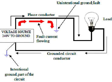
Fault is defined as a problem with an electrical circuit that does not operate properly. The problem is caused by physical damage to the system, faulty installation, faulty equipment or any other factors. In most cases, a very high current flow is associated with a fault. There are 2 types of faults; ground faults and short circuits. When a circuit allows current to flow to ground using a pathway other than the grounded circuit conductor, the circuit is said to have a ground fault.
Figure 16: Line ground fault
Figure 16 shows a line ground fault with low impedance to ground. The low impedance allows current in the circuit to increase. The red error shows the flow of fault current. This excessive current that flows in the circuit which causes many problems and dangers. Hence, this can superheat the air inside enclosures, eventually cause them to explode.
22
The second type of fault is short circuit. Short circuits differ from ground faults in one major way: they involve only the circuit conductors and no current is escaping from the circuit. In short circuit, the load is bypassed and the circuit conductor themselves represent the only impedance on the circuit as seen in Figure 17. The red arrow shows the fault current flowing to the ground. This short circuit has the potential to cause major damage to equipment such as burning and explosion.
Figure 17: Short circuit fault
23 2.4 Electronic Ballast Efficiency
The last objective is to perform analysis of electronic ballast. Nowadays, technology of electronic ballasts for fluorescent lighting system is moving fast and becomes the standard in the industry and further improvements continues to increase the performance of electronic ballasts. Electronic ballast offers a lot of advantages such as high frequency, reduce lamp flicker, less audible noise, extended lamp life time, light weight and control flexibility compared to magnetic ballast [25]. The performance of electronic ballast can be represented by power factor, input current, crest factor and ballast effieciency [26].
24
CHAPTER 3
RESEARCH METHODOLOGY
3.0 Procedure Identification
Figure 18 : Flow chart of the methodology of the project
Firstly, the research of the electronic ballast for normal environment and critical environment will be conducted. The electronic ballast is for saltwater environment application. Then, from the information and datasheets, electronic ballast will be simulated. NI Multisim will be used as the software to analyze the circuit. The bridge rectifier circuit is expected to produce a DC from the AC supply.
The inverter circuit will produce a high frequency square wave. If the simulation produces a desired result, then it will proceed with the stage of analysis the performance.Testing and troubleshooting will be carried out to verify the electronic ballast meets requirement. During this stage, there are several performance analysis need to be done such as output frequency, crest factor and efficiency.
25 3.1 Research on Electronic Ballast
Research is conducted to achieved first objective which is to understand electronic ballast system. Research paper is a thesis driven exploration of thoughtful reading on a particular subject. The reading material may come from several sources.
Conference proceeding papers are paper that represent by the researcher at the conference. The sources of these papers are from the internet which is IEEE Institute of Electrical and Electronic Engineers. Figure 19 shows the snapshot of IEEE website.
Figure 19: IEEE website snapshot
26
3.2 Research on Impact of Saltwater Environment to Electronic Ballast
The method for second objective is research on existing work on the effect of critical environment to electronic devices. Second method is to capture the problem for electronic device in saltwater application. Presently, the knowledge on corrosion issues of electronics are very limited [19]. There are some papers that discuss the effect of corrosion and environment on electronic circuits.
First paper reviewed is entitled “A review of corrosion and environment affects on electronics” [19]. This paper represents the important components in electronic devices that can be affected by the corrosion such as integrated circuits (ICs), printed circuit board (PCB), switches and etc. Also, discussion on material used in electronic systems, factor influencing corrosion, types of corrosion observed in electronics and testing methods.
Second paper is “ The impact of environment on corrosion of electric and electronic devices” [20]. This paper discusses the main corrosion failures and various criteria for adopting prevention and control measures.
Third method to study the impact of the environment to electronic devices as refered to Matco Service Incorporated website [6]. This website gives the info about material corrosion depending on the different environment. Figure 20 shows the snapshot of Matco Service Inc website.
Figure 20: Snapshot of Matco Service Inc website
27 3.3 Design Approach
The third objective is to design electronic ballast with protection scheme.
Fundamental circuit of electronic ballast must be constructed and compared with desired result. Then, another features of the circuit will be improved.
3.3.1 Required software:
Circuit simulation is important in circuit. By simulating the circuits, errors can be detected early in the process, and avoid costly and time-consuming prototyping. The most reliable software for the simulation is National Instruments Multisim Simulation as illustrated in Figure 21.
Figure 21: NI Multisim software view
28 3.3.2 Fluorescent lamp Specification:
Figure 22 shows fluorescent lamp that will be used in this simulation. In the simulation circuit, lamp will modeled as resistance. The category is T8 Fluorescent Tube and the rating is as follow:
Lamp nominal wattage: 36watt
Figure 22: Sample of T8 fluorescent lamp
29
3.3.3 Electronic Ballast Approach Circuit Diagram:
The basic circuit configuration of electronic ballast is shown in Figure 23.
The circuit design starts with basic circuit of ballast which consists of single phase voltage supply, series input resistor, full wave bridge rectifier, and a resonant circuit consist of capacitor C, inductor L and resistor R as a load. This circuit has dimming capability with the application of transistor [27]. The circuit will be modified to produce no dimming capability. This can be achieved by removing transistor. The resonant circuit oscillates at high frequency of 40 kHz amd high frequency harmonics are blocked by the input inductor [27]. If the series inductor increases, harmonic contents will reduce.
Figure 23: Circuit Configuration [27]
Figure 24 illustrates an expected output waveform of the full wave rectifier which is the input at voltage supply terminal of electronic ballast. Bridge rectifier provides full wave rectification.
30
Figure 24: Expected input and output waveform of full wave bridge rectifier [28]
The value of the DC output of bridge rectifier can be calculated based on the formula below. In case of full wave rectifier,
(1)
for both positive and negative half cycles. Hence;
Vdc = (2)
Therefore;
Full wave (3)
The root-mean-square (rms) value of load voltage is VL, which defined as : (4)
or
Full-wave (5)
The rectification ratio is : (6)
31
Series resonance circuit will be used in the ballast circuit. The resonance frequency is expected to be 40 kHz. The calculation of resonance frequency as shown below:
(7) Occurs when circuit is
(8) Resonance Frequency,
,
(9)
(a) at (a)at
Figure 25: Expected supply current and voltage [27]
Figure 25 shows the supply current and voltage of duty cycle 0.4 and at two different values of series inductor 30mH and 180mH. The values of supply inductor will give effect to the shape of sine wave input. Noticed that the electronic ballast has the advantages of making the power factor of the supply current almost unity.
32
Figure 26: Expected simulation result of lamp voltage during start up [27]
Figure 26 illustrates expected result of the lamp voltage during start up. The starting voltage should be very high initially then decreases as the lamp resistance decreases and takes steady state value during normal operation
Figure 27: Expected simulation result for the lamp voltage and current [27]
Voltage Current
Voltage Current
Voltage decreasing High start up voltage
33
Figure 27 shows the lamp voltage and current waveform at duty cycles 0.3 and 0.4 . The lamp current is nearly in phase with the lamp voltage and this ensures that the fluorescent lamp acts as a nearly resistive load at high frequency. The lamp current and voltage increase as the the duty cycle increases. Increasing the lamp current and lamp voltage as the duty cycle increases means power delivered to the lamp is increased and consequently the illumination of the lamp is increased as the duty cycle increases.
3.3.4 Improved Electronic Ballast circuit
Then, after the basic circuit design is completed and achieved desired result, design continues with advanced circuit which is called “self oscillating electronic ballast” or SOEB. The circuit is easily employed with integrated circuit driver, with well known features. But, when using self oscillating circuit, there will be improvements such as simplicity, low cost and low energy consumption [29]. The selection of suitable components, parameters and calculation will be determined. The complete circuit of SOEB is shown in Figure 21.
Figure 28: Proposed of self oscillating electronic ballast[30]
Lamp modeled as resistance
Resonant circuit
34
In this circuit, lamp is modeled as a resistance. SOEB is designed to drive 32 W fluorescent lamp at operating frequency 40 kHz supplied from 240V, 50Hz utility line. The RMS value of the fundamental component of inverter output voltage can be determined by expanding the square voltage in Fourier series , by
(10)
Vpp is the peak to peak voltage of the square waveform, delivered to resonant filter and load.
A square waveform voltage to the resonant circuit when zener diodes change their polarity and connecting zener diodes Iz current and Vz voltage. Bridge rectifier that formed by D1-D4 and the capacitor CB are responsible to produce a continous voltage. Through this voltage, capacitor CQ is charged by resistor RQ. When voltage of CQ reachs diac avalanche voltage, a pulse between gate and source of M2 is applied. So, the current will be flowing to the resonant circuit that formed by Cs, Ls
and Cp. Lp winding is in series with the filter form withLs1, Ls2, and zener diode Dz1- Dz4 , the self oscillating gate driver.
The current through Lp is reflected to Ls1 andLs2, switching MOSFET M1 and M2 of the asymmetric half bridge inverter. A high frequency Vab square wave voltage, feeds the parallel resonant LCC filter used for lamp ignition and current stabilisation in steady state. Resistor Rm is to ensure initial condition for the capacitor of resonant circuit and M2 conduction for ignition. The diode D5 is used to avoid improper diac conduction and simultanneous conduction of M1 and M2 after lamp ignition.
35 Design specification:
Table 6: Design specifications of electronic ballast
Component Specification
Cs Polypropylene capacitor,
147nF/400v
Cp Polypropylene capacitor,
6.8nF/1.2kv
Ls Resonant inductor, 2.275mH, 137
turns on core EE 20/10/5 1300- 1P12R-Thornton
Cff Polypropylene capacitor,
15nF/400v
Rff Resistor 6.8kΩ, 1/8W
Lp, Ls1,Ls2 Current transformer Lm=20mH, 300/70/70 turns on core EE 30/15/7 1800-IP12R-Thornton
Diac DB3
Rq Resistor 220kΩ, 1/8W
Cq Ceramic capacitor 100nF/63V
Rm Resistor 470kΩ, 1/8W
Ds UF4007 Diode
M1,M2 IRF740 Mosfets
D1-D4 1N4007 Diodes
R Lamp 32 W
CB Electrolytic capacitor, 100μF
36
Table 6 shows the design specification of electronic ballast circuit. The specification may vary depends on the desired output. The circuit will be re-designed until desired output is obtained.
Figure 29: Gate source voltage waveform of one Mosfet [30]
Figure 30: Current waveform of RLC series filter [30]
Figure 29 shows the gate-source voltage on one of the Mosfet of Half Bridge Inverter.
Figure 30 shows the branch of series resonant RLC current.
37
Figure 31: Current and voltage on LCC output filter [30]
Figure 32: Current and voltage of fluorescent lamp [30]
Figure 31 shows the current and voltage of LCC output filter. Figure 32 shows the fluorescent lamp voltage and current.
38
Figure 33: Mosfet voltage and current waveforms [30]
Figure 34: Voltage and current waveform during the fluorescent lamp start up [30]
The fluorescent lamp voltage start up is shown in Figure 34. During the start up, the voltage is maximum in order to ioniz the gas inside the tube. But, the current still maintain at lower value. This is clearly showned that the function of the electronic ballast is to limit the current. Then, the lamp would not be destroyed by the high current. After the tube has completely ionized, the voltage will be decreased just enough value to keep the lamp lit. Also, current maintains when the lamp has reached steady state condition.
Steady state condition Maximum voltage at start up
39 3.3.5 Cut off circuit
After the research, electronic ballast used for saltwater environment is not much different from regular electronic ballast. Their casing if different based on the explosion proof standard EX. The casing needs to be robust, water proof and not rust.
In this case, the electronic ballast is damaged at the input power supply. The use of cut-off circuit at the input terminal is imperative. The circuit needs to be high sensitivity, simple and robust. For the protection scheme, electronic circuit breaker or cut-off circuit can be added at the input terminal for short circuit protection.
Figure 35: Short circuit breaker circuit
The output of the short circuit protection must be 240 V in order to give enough voltage to elctronic ballast to operate. This kind of circuit breaker is low cost and easy to construct. The circuit will protect the equipment against a possible short circuit conditions. The circuit operation is a follow. The sensing element of the circuit is optocoupler and it is the heart of the whole system. Opto-coupler consists of an LED and a switching transistor arrangement internally. The transistor will switch ON in response to the LED illumination. Thus, triggering of the transistor which forms the output of the device takes place without any physical or electrical contact rather through the passage of light rays from the LED.
40
The built in LED is the input of the device to switched the transistor of the opto-coupler. In this circuit, bridge network supply the voltage to opto-coupler LED which is voltage source from the potential generated across resistor R1.
Resistor R1 is connected in such a way that AC mains current to the electronic ballast wiring passes through it and therefore any overload or overcurrent is subjected to the R1. During an over load or short circuit conditions, R1 quickly develops a potential across it which is rectified and sent to the opto-coupler LED.
The LED immediately illuminates and switching ON the corresponding transistor.
Refer to the circuit in Figure 35, opto transistor’s emitter is connected to the gate of an external SCR, whose anode is further connected to a TRIAC’s gate. During normal operation, TRIAC remains ON allowing the load connected across it to remain operational.
This is because SCR also remains OFF and allows the TRIAC to acquire its gate current through R3. However, in case of an overload or a short circuit, as mention in literature review, the optocoupler transistor conducts and triggers the SCR. This instantly pulls the gate potential of the TRIAC to ground, inhibiting it from conducting. TRIAC immediately OFF, safeguarding the load and the house wiring to which it is configured. SCR remains latched , until the problem is rectified and the circuit is restarted. The section that consists of C1, Z1 and C2 is a simple transformerless power supply circuit used for powering SCR and TRIAC. The circuit is design based on the following parameters.
41 Design specification:
Table 7: Design specification of short circuit protection Component Name Specification
Vin
R1 Resistance is calculated to produce 2 V across it at the determined critical load condition
R2,R3,R4
R5
R6
C1,C2
SCR C106
TRIAC BT136 or higher rating OPTO-COUPLER MCT2E
ZENER
DIODES 1N4007
Table 7 shows the design specification of the circuit. The specification stated may vary depends on the desired output. The output should be same with the input supply. The circuit will be re-designed until desired output is obtained.
42 3.3.6 NI Multisim Simulation
The purpose of the simulation is to check whether the circuit meet the expection result. After the circuit with parameters as shown in the design specification constructed, the waveforms will be observed. This is to ensure the correct output from the designed circuit can be identified if the waveform do not indicate the correct result, the circuit will be re-designed either by changing the parameters values.
3.4 Performance Analysis
The last method is for fourth objective. Fourth objective is to analyze the efficiency of the circuit.
1. Efficiency: Efficiency is a term to describe level of effectiveness of the ballast.
Efficiency which describes ballast performance, is used for a no dimensional quantity [31]
2. Input Waveform: Obtaining the input waveform will enable to determine current crest factor.
(11)
American National Standard Institute (ANSI) specification requires that lamps to be operated with crest factor equal to or less than 1.7, sine wave has a crest factors 1.4 [30]. Higher crest factor tends to reduce lamp life span. Determining the waveform of the ballast input supply will enable the input estimation and current distortion. Both voltage and current should be in sinusoidal form. Any distortion of the current waveform will distort voltage in electrical system, therefore reduce power factor.
(10)
43 CHAPTER 4
RESULT AND DISCUSSION
This chapter will elaborate on the findings gathered for this project. This chapter will perform all the method that mentioned in methodology section. Based on the result occurred, I would discuss about the performance of the circuit and any things that related with the project. The construction of the ballast circuit is done in stages. Starting with bridge rectifier, then followed by self oscillating drive and lastly is resonant circuit. The output will be recorded at each stage to give clear function of every stage of electronic ballast.
4.1 Bridge Rectifier
The following waveforms are the simulated results for circuit Figure 10 (full bridge). As required, the wave is full rectification. The result for calculation is shown in Figure 36.
Figure 36: Output voltage of bridge rectifier T
Rectifier output voltage =338.6V @ Vm
44
From equation (1) – (6), information obtained as follow.
DC voltage that has been produced is 216V RMS load voltage that has been produced is 240V The rectification ratio is 81 %.
=
The output frequency of rectifier is equal to the input frequency.
Figure 36 shows the output voltage of the bridge rectifier. The output voltage should produce full wave rectification. RMS voltage is 240V. The output frequency of the rectifier is equal to line frequency. The function of rectifier is to produce DC voltage as supply to self oscillating driver. But, the waveform is not smooth DC. The solution is by adding capacitor in parallel with diode. A 100μF of capacitor is enough to produce smooth DC going. Figure 37 shows the smooth DC voltage waveform.
DC current of rectifier is 10 mA. The DC current calculation as shown below.
Figure 37: Smooth DC voltage with CB=100μF
Smooth DC voltage = 338V
45
46 4.2 Electronic ballast fundamental circuit
Electronic ballast fundamental circuit consists of rectifier and resonant circuit. For resonance circuit, it is expected to produce 40 kHz output frequency. The parameters of the circuit is determined by the following formulas. The simulation results are based on the circuit in Figure 18
For , choose So,
Figure 38 and Figure 39 show the input voltage and current of ballast circuit by using Ls= 30mH.
Figure 38: Simulation result for supply voltage L=30 mH
Figure 39: Simulation result for supply current L=30 mH
Vin = 339.4v
Iin = 323.2mA
47
The maximum voltage of the supply is 339.4 V. The maximum supply current is 323.3mA. Figure 40 and Figure 41 show the voltage and current supply at L=180mH.
Figure 40: Simulation results for supply voltage L=180mH
Figure 41: Simulation results for supply current L=180mH
Noticed that electronic ballast has the advantage of making the power factor of the supply current almost unity. This can be seen by changing the value of inductance, does not effect the value of current .
Iin=338.3
Iin=338.5
48
4.3 Improved electronic ballast circuit with power supply cut-off circuit Figure 42 and Figure 43 show the improved electronic ballast circuit with power supply cut-off circuit. The self oscillating circuit is added to basic ballast circuit.
Figure 42: Power supply cut-off circuit
Figure 43: Self oscillating electronic ballast circuit
49 4.3.1 Electronic Ballast Simulation
4.3.1.1 Bode plot of LC Series Resonant Circuit
Bode plot is useful method to represent the gain and phase of a system as a function of frequency. This is referred to as the frequency domain behavior of a system. This section is analysis of LC resonant circuit of the self oscillating electronic ballast. The parameters value of Ls, Cs and Rlamp are same as in Table 6. The circuit configuration is shown in Figure 44. The resultant bode plot is shown in Figure 45.
Figure 44: LC series configuration
Figure 45: Bode plot of LC Series Circuit
50
From the designed circuit,series LC circuit is expected to produce 40kHz output frequency. The line voltage is 240V and line frequency is 50Hz.
51 4.3.1.2 Self oscillating driver
The simulation of self oscillating electronic ballast is done by using NI Multisim software. The simulation result is slightly different with desired result because of the component selection. The limitation of the software cause the actual result differ with desired result. Input voltage to the self oscillating driver is supplied by bridge rectifier circuit which is 240V. Figure 46 shows the voltage measured at one of MOSFET gate-source terminal.The value of pulse voltage is +10V and -12V. Pulse voltage is the switching voltage of the MOSFET.
Figure 46: Simulated voltage waveform of gate-source MOSFET (10V/div, 20ms/div)
-12V +10V
0
Delay 30s
Transient Analysis for 600s
52 4.3.2 Cut off Simulation
The conventional electronic ballast has been improved by adding power supply cut off at the input terminal. This circuit is added to solve the problem at section 1.2.
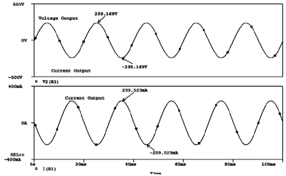
Figure 47: Voltage and current waveform of the lamp
From the observations, output of power supply cut-off circuit affected by the load.
The output voltage is vary when the load is connected. Figure 50 shows the output voltage of power supply cut-off circuit without connecting to electronic ballast. The voltage is equal to the input voltage.
53
Figure 48: Output voltage of power supply cut-off circuit without connecting to electronic ballast
Output voltage = 240V
54
CHAPTER 5 CONCLUSION
The task for research is completed. Some of the journal and research papers that are relevant to the topic have been reviewed. In order to get the best result, the comparison of all the journal and research are necessary. The simulation of the circuit is started with basic circuit then basic circuit diagram will be improved by adding some other features such as self oscillating driver. Simulation of electronic ballast driving a fluorescent lamp at high frequency is carried out using NI Multisim software programme.The simulation result is compared with desired result.
Troubleshooting stage is the most important stage. In order to get correct result, every parameter need to be observed such as voltage and current. In the future, it recommended to carry out with experimental result.

![Figure 6 : Schematic of traditional ballast in series with inductor and capacitor [8]](https://thumb-ap.123doks.com/thumbv2/azpdforg/11176075.0/18.892.289.683.113.372/figure-6-schematic-traditional-ballast-series-inductor-capacitor.webp)