Inquiries regarding the use of the book should be addressed to the Rights and Permissions Department of INTECHOPEN LIMITED ([email protected]). A Concise Testimony to Advances in Condensed Matter Physics One of the important topics in the emerging field of physics is condensed matter.
A succinct testimony of advances in condensed matter physics One of the important topics in the protuberant area of physics is condensed
There is a wide variety in the branch of condensed matter physics, such as crystallography, metallurgy, elasticity and magnetism. Studies on condensed matter physics show significant properties in solid materials, especially at the atomic scale.
Topical advancements in recent advancements in the field of condensed matter and materials physics
Current Advances in Recent Advances in the Field of Condensed Matter and Materials Physics condensed matter and materials physics. The entire perception of contemporary technology is based on the ideologies of condensed matter and material physics.
Conclusion
The Fermi-Hubbard model is a key concept in condensed matter physics and provides important insights into electronic and magnetic properties of materials. Viral shells—study the condensed matter physics to the assembly and maturation of viral capsids [30].
Introduction
In this chapter, we provide a current summary of recent frontline research progress related to excitons in atomically thin 2D materials and vdWHs. Afterwards, we introduce several representative optoelectronic and photonic applications based on excitonic effects of 2D materials.
Exciton physics in 2D semiconductors and insulators
Excitons, trions, biexcitons, and interlayer excitons
Excitons can be bright or dark depending on the spin orientation of the individual carriers: the electron and the hole, as shown in Figure 2(b). Similar to monolayer excitons, interlayer excitons can also be either bright or dark depending on the spin and momentum of the states involved [ 49 , 50 ].
Excitons in atomically thin 2D materials
Due to significant Coulomb interactions in 2D materials, an exciton can capture an additional charge to form a charged exciton known as a trion, a localized excitation composed of three charged quasiparticles (Figure 2(c)). In addition to the intralayer excitons mentioned above, interlayer excitons, where the involved electrons and holes are located in different layers, can also be formed in bilayer or few-layer 2D materials, especially in vdWH due to the strong Coulomb interaction (Figure 2 (e)).
Excitons in vdWHs
When higher order excitonic quasiparticles form, more energy is required i.e. the binding energy of trion or biexciton. For the two signature relaxation processes in vdWHs (that is, the population decay of optically excited excitons and the exciton spin valley lifetime that determines the information storage time in the spin valley degree of freedom), they are both significantly longer than the case of a single layer.
Tuning methods of excitons
- Electrical tuning
- Magnetic tuning
- Optical tuning
- Mechanical tuning
Another work demonstrated the continuous tuning of the exciton binding energy in monolayer WS2 field effect transistors, finding the ground and excited excitonic states as a function of the gate voltage [87]. A schematic representation of the valley polariton phenomenon is shown in Figure 10(c), where the micro-cavity structure consists of silver mirrors with a silicon dioxide cavity layer embedded with the WS2 monolayer.
Optoelectronic devices
Electroluminescent devices
The funnel effect is a rare method to control the motion of excitons, paving the way to create a continuously varying band gap profile in initially homogeneous, atomically thin 2D materials. The funnel effect is a rare method to control the motion of excitons, paving the way to create a continuously varying band gap profile in initially homogeneous, atomically thin 2D materials.
Photovoltaic solar cells
For impact excitation devices, excitations are generated by impact excitation of excitations in the high-field regime rather than bipolar recombination. For bilayer emission devices, emission occurs due to the recombination of electrons and holes residing in the adjacent layers.
Photodetectors
To enhance the light absorption of 2D semiconductor photovoltaic cells in the ultra-thin limit, light-trapping designs are needed, such as using plasmonic metal particles, shells, or resonators to amplify photocurrent and photoluminescence. For graphene-based photodiodes, the earliest reported photodiodes are metal-graphene. metal photodiodes, in which photocurrent was generated by local illumination of the metal/graphene interfaces of a back-gated graphene field-effect transistor. a) Scheme of a graphene hybrid photoconductor [141].
Summary and perspective
Binding energies and spatial structures of small carrier complexes in monolayer transition metal dichalcogenides via Monte Carlo diffusion. Polarization switching and electrical control of excitons between layers in two-dimensional van der Waals heterostructures.
Excitonic and biexcitonic properties in low-dimensional semiconductors
Excitons and biexcitons in two-dimensional semiconductor structures This section presents a subject of an enormous significance for the excitons
The promising area of excitonics represents the science and production of the excitons in disordered and low dimensionality semiconductors (organic. Several researchers have shown that with the emergence of the exciton binding energy value in low dimensional semiconductor systems, the biexciton binding energy.
Excitons and biexcitons in one-dimensional semiconductor structures One-dimensional semiconductor structures have obtained a remarkable consid-
Various theoretical and experimental analyzes have been developed to improve excitonic devices using IX propagation in different types of single QWs and coupled QWs [92, 93]. 103] provided a valuable survey on the special features of long-lived exciton, trion, and biexciton cases in CdSe/CdTe colloidal QWs and proposed a new light collector model with minimal energy losses.
Excitons and biexcitons in zero-dimensional semiconductor structures Zero-dimensional semiconductor structures have captivated a notable interest
In the conditions of cryogenic temperatures, an increasing quantum yield of photoluminescence was reported under the conditions of incorporation of a WSe2 layer into a three-layer composition in contrast to the case of two-layer heterostructures. In this context, some researchers have elucidated the role of indirect exciton expansion (indirect exciton — IX — is a bound electron-hole pair in separate QW layers [89]) observed in vdW transition metal dichalcogenide (TMD) heterostructures at room temperature, and this study helps to advance exciton devices with energy-productive computation and ideal link quality for optical communication cases [90, 91]. ].
Conclusions
Excitonic states in semiconductor quantum dots within the framework of the modified effective mass method. Optical spectroscopy of excitons with spatially separated electrons and holes in nanosystems containing dielectric quantum dots.
Classification and preparation of amorphous semiconductors Amorphous semiconductor can be classified as tetrahedral-bonded Si like a
The binary alloys of amorphous semiconductors are technologically important materials because of their direct and rather large gaps [24]. Classification and manufacture of amorphous semiconductors Amorphous semiconductor can be classified as tetrahedrally bonded Si as a.
Band models of amorphous semiconductors
- Cohen-Fritzsche-Ovshinsky (CFO) model
- Davis and Mott (DM) model
- Street and Mott model
- Kastner Adler and Fritzsche (KAF) model
Defects in the random network, such as dangling bonds, vacancies, etc., result in a band compensation level near the middle of the gap. In 1975, Emin [33] proposed that charge carriers in an amorphous semiconductor can go into self-trapped states (small polarons) as a result of polarization in the surrounding lattice.
Preparation of amorphous semiconductors 1 Melt-quenching technique
Thermal evaporation technique
The material placed in the boat should have a low melting point than the molybdenum, which can evaporate easily and spread evenly on the substrate. An oil diffusion pump capable of producing a vacuum of 10−6 Torr in the chamber must be maintained for the vaporization of materials.
Basic properties of amorphous semiconductors 1 Structural properties
Electrical properties
The band conduction occurs when the carriers will excite outside the mobility edges in non-localized states. The transport above Ec is the band conduction type for electrons and the transport below Ev is band conduction for holes.
Optical properties
Little variation in bond length and bond angle and other imperfections result in broadening of the bond edges. In an indirect bandgap semiconductor, the maximum energy of the valence band occurs at a different value of momentum than the minimum of the energy of the conduction band (Figure 7).
Results
At low temperature, conduction occurs by thermally assisted tunneling of carriers between the localized states near the Fermi energy EF. At low temperature, conduction occurs by thermally assisted tunneling of carriers between the localized states near the Fermi energy EF.
Conclusions
The increase in the optical gap upon the addition of sulfur to In-Se thin films may be due to the reduction of disorder in the system and also to the reduction of the density of localized states. Prediction of the effect of additives on the density of valence alternation centers in lone pair semiconductors.
Historical evolution of the traveling-wave parametric amplifiers The theory of a new concept of microwave amplifier was developed by Cullen
Historical evolution of the traveling wave parametric amplifiers The theory of a new concept of microwave amplifier was developed by Cullen. The study of the collective behavior of groups of Josephson junctions forming a transmission line has been an active field of study of several theoretical works [21, 22].
Theoretical models for a 4WM process in a TWJPA
- The classical theoretical model
- Quantum Hamiltonian model based on continuous-mode operators
- Quantum Hamiltonian model based on discrete-mode operators
- Models comparison
An alternative approach for deriving the TWJPA quantum dynamics is proposed in [32]. Therefore, the quantum Hamiltonian of the system can be expressed with a first nonlinear order approximation as
Conclusions
Detailed calculations of the output state of a TWJPA in the case of a single photon input state and in the case of a coherent input state are presented for example in [32]. This work was partially funded by the Joint Research Project PARAWAVE of the European Metrology Program for Innovation and Research (EMPIR).
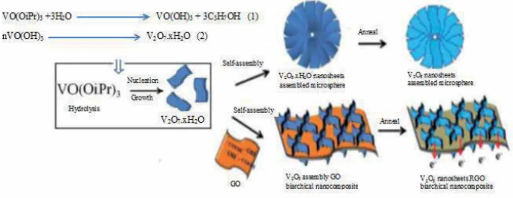
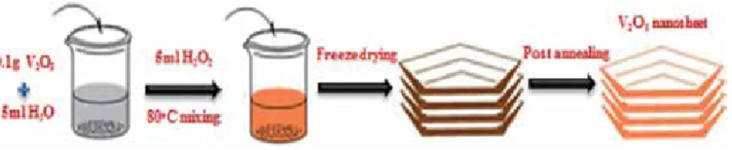
Vanadium oxide nanosheets’ preparation and characterization by SEM and TEM
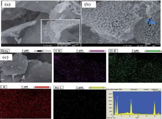
Schematic representation of the formation of 3-D nanosheets of V2O5/hierarchical RGO nanocomposite [14]. Surfaces act as reaction centers. The inset in (a) shows the profile of a single nanocomposite sheet; (c) SEM image of V2O5 nanosheets/RGO hierarchical nanocomposite with corresponding EDS maps of V, O and C elements (Au is from sputter coating) [14]. a and b) TEM images of V2O5 nanosheets/RGO nanocomposite at different magnifications; (c) HR-TEM image of V2O5 nanosheets/RGO nanocomposite; and (d) selected area electron diffraction (SAED) pattern [14].
Nickel oxide nanosheets preparation and characterization by SEM and TEM
By reducing the amount of sodium oxalate to 0.022 g, nanoparticles of NiC2O4.H2O were generated as shown in Figure 2b [46]. By reducing the amount of sodium oxalate to 0.022 g, nanoparticles of NiC2O4.H2O were generated as shown in Figure 2b [46].
Zinc oxide nanosheets preparation and morphology study by SEM and TEM
A schematic diagram of the growth of ZnO nanostructures fabricated by the hydrothermal preheating method is shown in Figure 14. The SEM image shown in Figure 15(a) demonstrates that the sample obtained after 12 hours of preheating has a high-density ZnO architecture that grows uniformly and is highly dispersed in the substrates without any aggregation, thus achieving high yield and good uniformity. state of manufacture [48].
Conclusion
Template-less synthesis of ultra-large V2O5 nanosheets with exceptionally thin thickness for high-performance lithium-ion batteries. Carbon nanotube promoted Co-Cu catalyst for highly efficient synthesis of higher alcohols from syngas.
Modification of graphene with self-assembled monolayers
Surface charge transfer depends on the relative energy of the dopant's highest occupied molecular orbital (HOMO) or lowest unoccupied molecular orbital (LUMO) relative to the Fermi level of graphene. This clearly indicates a modification of the electronic properties of graphene that becomes available by suitably modifying the SAM techniques.
Applications of graphene/SAM structure
Biosensor
The monolayer can also be used as a physical separator in order to improve the sensory properties of the layer below. The measured fluorescence spectra showed that the increase in intensity was related to the concentration of the target molecule ( Figure 3 ), and linear correlation was obtained using GO, which was necessary for defining the device as a sensor [ 35 ].
Device
This process effectively increased the conductivity of graphene. a) Optical microscope (b) SEM images of the open contact graphene device. The same group also used APTES as a SAM molecule and 2,3,5,6-tetrafluoro-7,7,8,8-tetracyanoquinodimethane (F4-TCNQ) as a doping agent to modify the properties of graphene and examined the thickness of F4-TCNQ related to the properties of the graphitic bilayer F4-TCNQ in the double graphs F4-TCNQ in relation to the electrical properties of graphitic F4-TCNQ 2/3AMSO2-H. As a substrate.
Interface modifier
This process allowed the surface modification for the contact angle to be low enough to achieve complete wetting that causes the GO suspension to adhere to the Au surface (Figure 16a) [53]. To increase the hydrophobicity of the film, an OTS-SAM outer layer is introduced, which reduced the friction and increased the anti-wear life [61].
Spacer
Graphene synthesis by SAM
Work function engineering of self-assembled monolayer graphene electrodes for high performance organic field effect transistors. A multivariate curve resolution evaluation of an in-situ ATR-FTIR spectroscopy study of the electrochemical reduction of graphene oxide.
Simulation procedure and stress calculation
Wu et al. [18] performed MD simulation to investigate the effects of temperature, charge and discharge rate, dwell time, and composition of Ni-Al alloys on the nanoimprint lithography process. Geometries of models with three different well shapes: (a) rectangular well, (b) spherical well, and (c) Berkovich well.
Simulation results and discussion
Effect of indenter shapes on load: Displacement curves
Finally, the atomic configurations and their evolutions are observed by the visualization tools, AtomEye [34], which details the microstructural evolution of nanoindentation. The stress tensor for an atom is calculated as a time-averaged value over a number of time steps after relaxation from a compression step, because atom α of the atomic stress tensor is defined as [35, 36]:.
Effect of indenter shapes on stress distributions
For a Berkovich indenter, the force acting on the indenter slowly increases with the increase in penetration depths, the load drops are usually small or not noticeable. Although the load for the Berkovich indenter is the smallest of the load-displacement curves in Figure 2, the contact area of the indenter is also the smallest, resulting in a voltage value that is still high near the indenter.
Effect of indenter shapes on surface and internal microstructures of specimen To understand the microstructure evolution of the specimen during nanoinden-
When the unloading is completed, the indentation returns to its original place, the stress cannot be fully recovered, and there are still many dislocations on the surface of the sample for the cases of rectangular and spherical indentation, and these dislocations move slowly towards the surface and the boundary of the sample during unloading, as in the form of microspection, as shown in Fig. in the case of the Berkovich indenter, there is almost no displacement of the sample surface at the finished unloading site (see Figure 5c). For the Berkovich indenter, a sudden increase in stress near the indentation and other parts of the specimen is very low, which is the reason for the sharp indentation stress concentration.
Jitter Effects on Chaotic
Mathematical model
- Basic state
- Perturbed state
T¼T0þΔT at z¼0 and T¼T0 at z¼d, (8) where q�> is the velocity of the fluid,Ω�> is the vorticity vector, p�> is the fluid pressure,ρ�> is the density,ν�> is the kinematic viscosity, the ratio is the KT� and diffusivity, is the ratio rmal expansion coefficient. T¼T0þΔT at z¼0 and T¼T0 at z¼d, (8) where q�> is the velocity of the fluid,Ω� > is the vorticity vector, p� > is the fluid pressure,ρ� > is the density,ν�> is the kinematic viscosity, and� is the kinematic viscosity and � ratio rmal expansion coefficient.
Truncated Galerkin expansion
In the basic state, we superimpose the perturbations on the shape. 4)–(7) and using the ground state solutions, we obtain the equations governing the perturbations in the form 4)–(7) and using the ground state solutions, we obtain the equations governing the perturbations in the form
Stability analyses
- Dissipation
- Equilibrium points
Stability of equilibrium points
- Nusselt number
To understand the stability of the system, we determine the fixed points of the system and will try to find the nature of these fixed points through eigenequation. The characteristic values of the above Jacobian matrix, obtained by solving for the zeros of the characteristic polynomial, provide the stability conditions.
Result and discussion
The plate consists of two different dielectric layers with a dielectric interface that is periodically corrugated in the transverse direction of the waveguide (in the direction perpendicular to the direction of wave propagation). In the second part of this chapter, we present calculations of the induced inhomogeneous electric field of the wave near the corrugated dielectric interface.
Wave electric fields in an open waveguide with a plate consisting of two dielectric layers with a corrugated interface
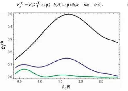
The first harmonic electric field of the vibration is smaller for both the higher and lower vibration amplitude. So we have the expression for the x-component of the first harmonic electric field of a wave at y¼R (in the region where the conducting channel is).
Electron interaction with electromagnetic wave
More precisely, the electron drift speed must slightly exceed the phase speed of the electromagnetic wave [7].). Due to the change of the electron velocity in the electric field, the electron flow becomes velocity modulated.
Conclusion
Electrons in the conducting channel move in the transverse direction of the waveguide (in a direction perpendicular to the direction of wave propagation). The floating electrons interact with the inhomogeneous electric field induced near the dielectric interface by the TE wave of the waveguide.