Inquiries about the use of the book should be directed to INTECHOPEN LIMITED rights and permissions department ([email protected]). The publisher accepts no responsibility for any damage or injury to persons or property resulting from the use of any materials, instructions, methods or ideas contained in the book.
Synthesis methods of 2D materials 1 Graphene
Tungsten disulfide (WS 2 )
Molybdenum disulfide (MoS 2 )
Applications of 2D materials 1 Graphene
Tungsten disulfide (WS 2 )
Molybdenum disulfide (MoS 2 )
Graphene is widely used for a variety of applications, including energy storage, solar cells, and gas sensing. We recently demonstrated a new type of graphene gas sensor based on the AC electroluminescence (EL) principle [4].
Conclusion
Most applications of Si3N4 have been used in terms of improving properties such as surface modulation for orthopedic applications [25] and bio-medical applications [26]. Layer-controlled, wafer-scale, and conformal synthesis of tungsten disulfide nanosheets using atomic layer deposition.
Introduction
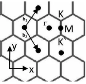
The chiral vector Ch is usually written from the two integers n and m as. According to the manufacturer's (Graphene Supermarket™), structural analysis for fluorinated graphene nanosheets (GNPs), the lateral dimensions of the wrinkled sheet-like outer surface of the GNPs are ~1–5 μm [ 6 ].
Experimental
Graphene nanoplatelets (GNPs) are usually produced by intercalation of graphite in various ways, followed by an acid cleaning process and further exfoliation of the original GNP flakes [9]. The modular software program Gwyddion was used to generate three-dimensional visualization of the aggregate structures of the nanoplates.
Results
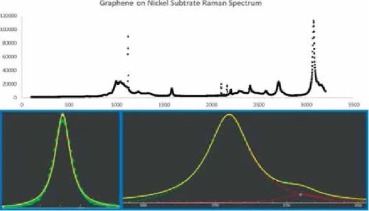
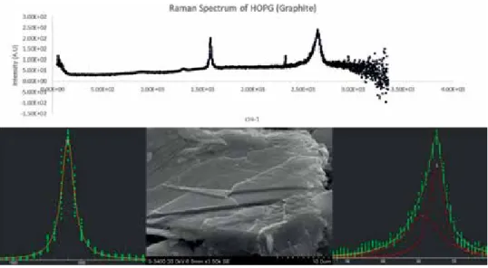
In the case of graphene, the G′ band has a greater intensity than the G band, which is the case for G bands illustrated in Figures 7 and 8 . The G′ band of graphite is also shifted to a higher frequency compared to that of graphene [11]. The absence of the peak (103) in the undoped sample is considered as the doping concentration increases. The direct and indirect band gap of the co-doped ZnO thin film is shown in Figure 8.
The transmittance of the films increases from 68.5 to 83.5% and then decreases as the doping concentration increases. The direct and indirect band gap of the Co-doped ZnO thin film is shown in Figure 8. The transmittance of the films increases from 68.5 to 83.5% and then decreases as the doping concentration increases.
In the case of Y-doped ZnO thin films, the electrical resistivity of the film first decreases and then increases as the Y doping concentration increases [26].
Kinetics and thermodynamics of g-SiN formation on the Si (111) surface
Formation kinetics of silicon nitride
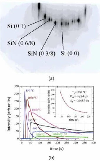
In our experiments, silicon surface nitridation starts with the initiation of ammonia flux on the pure Si (111) substrate heated to temperatures above 750°C [25]. As an example, the inset in Figure 1b shows the fit of the experimental curve to the exponential law at T = 1050°C. Inset Figure 1b shows the approximation of the kinetic curve obtained at T = 1050°C (gray, solid) by the exponential function (red, dash).
Since the rate of formation of the structure (8 × 8) is high during the nitridation process, the equilibrium concentration of mobile adatoms Sia does not have time to establish and the coverage of the surface by the two-dimensional phase (8 × 8) is determined by the initial concentration of mobile silicon adatoms at the Si surface at a given temperature. It should be emphasized once more that the formation of the (8 × 8) structure arises from interaction of ammonia with the mobile silicon adatoms rather than the dangling bonds of silicon atoms incorporated in lattice site (i.e. immobile) on the Si (111) surface.
Thermal decomposition of a two-dimensional layer (8 × 8)
The inset of Fig. 2a shows the energy diagrams: the solid curve corresponds to the formation and decay of the (8 × 8) structure, and the dashed–dotted curve to the formation of amorphous Si3N4. Since the activation energy of decomposition cannot be less than the heat of formation (that is, Ea ≥ ΔH), then the heat of formation of the structure (8 × 8) ΔH is not greater than 4 eV. The inset of Fig. 2a schematically shows the relationship between the heat of formation and the activation energy of the thermal decomposition of the (8 × 8) structure, and also shows the energy diagram of the formation of the Si3N4 amorphous phase.
In our case, at a much lower temperature, T = 1055°C, the complete decay of the (8 × 8) structure takes about a minute, confirming the lower thermal stability of the (8 × 8) structure compared to the β-Si3N4 crystal. The activation energy for the decomposition of the (8 × 8) structure measured here coincides with the activation energy of the thermal surface decomposition of β-Si3N4 (93 kcal/mol), but the pre-exponential factor s) is 106 times higher than the pre-exponential factor for β-Si3N4 surface decomposition.
Comparative STM/STS study of the (7 × 7) and (8 × 8) structures on the Si (111)
When the Si-N bonds are broken, the formation of activated nitrogen atoms N* weakly bound on the surface and after the formation of N2 molecules (N* + N* = N2) occurs. Thus, the structure (8 × 8) at a temperature above 980 ° C is destroyed, both during exposure to vacuum and during the continuation of the nitriding process under the flow of ammonia, when it turns into amorphous Si3N4. Therefore, the experimental data on the transformation to an amorphous phase and thermal decomposition evidence the metastability of the (8 × 8) phase, in contrast to the stable crystalline phase of β-Si3N4 or the amorphous phase of Si3N4.
STM/STS of the structure (8 × 8)
The atomic structure of the pristine surface (7 × 7) and the surface with chemisorbed ammonia on Si(111) (obtained at 750°C, 4 min, PNH3 = 10−7 Torr) were investigated in real space by scanning tunneling microscopy (STM). We performed scanning tunneling spectroscopy (STS) measurements of a clean surface (7 × 7) and on a chemisorbed ammonia surface (Figure 4c). The size of the hexagonal side in the STM images represented by the authors (see Figure 5a and b in the article [24]), as well as in our case, was about 6 Å.
Consequently, the honeycomb structure detected in this work and in the work [24] does not correspond to the structure of the β-Si3N4. It seems that in most studies devoted to STM of the (8 × 8) structure, only the adsorption phase has been clearly observed, because usually the ordering of the structure is not very high due to the mobility of adatoms (see, therefore, the 6 Å honeycomb structure has not been considered until now in the modeling of (8 × 8) structure.
HRTEM study of van der Waals structure of silicon nitride and aluminum nitride
Moreover, in the works [48, 49] devoted to the calculation of electronic states (0001) β-Si3N4, no HOMO states related to dangling bonds were found. As will be shown further, it is better to associate this peak in the density of states (8 × 8) with π band.
Graphene-like models of the structure (8 × 8)
HRTEM study of the van der Waals structure of silicon nitride and aluminum aluminum nitride. The interplanar spacing on the Si substrate in the silicon nitride and AlN layers was determined, see Figure 7. Van der Waals and Graphene-Like Layers of Silicon Nitride and Aluminum Nitride DOI: http://dx.doi.org/10.5772/intechopen.81775.
If only the silicon nitride layer had dangling bonds (either silicon or nitrogen), then the AlN layer would have formed in the bulk wurtzite structure (formation of graphene-like AlN is discussed below). Possible graphene-like models of the g-Si3N4 and g-Si3N3 silicon nitride layer are shown in Figure 8.
Graphene-like AlN layer formation on Si (111) surface by ammonia MBE
We observed the appearance of AlN diffraction spots and the transformation of the (8 × 8) structure into a new quadruple structure. The increase in lattice constant from 3.08 to 3.09 Å under Al flow without ammonia flow (i.e., no AlN growth) is clearly visible. The lateral size of the g-AlN islands was estimated from the RHEED data as
The fractional streaks of the (4 × 4) structure gradually dim along with the increase in fundamental (0 1) g-AlN streak intensity. The value 3.125 Å corresponds to the bulk value of the wurtzite AlN lattice constant at high temperature [52].
Conclusion
The thermal decomposition kinetics of this two-dimensional silicon nitride layer was studied. As a result, the polarizability and dielectric function are shown to strongly depend on the direction of the transferred moment. As a result, the polarizability and dielectric function are shown to strongly depend on the direction of the transferred moment.
In the range of 0.2≤ q≤0.5 (1=Å), there is a clear dependence of the dielectric function on the direction of the transferred momentumq. At absolute zero temperature (T = 0) and with free carrier density corresponding to chosen Fermi energyEF, we presented numerical results for Re[ϵðq;ω¼0Þ] in different directions of the transferred momentumq.
Thin Films for Photo-Voltaic Applications
Experimental methods and results 1 RF sputtering
- Scanning electron microscopy
- Transmission electron microscopy and atom probe tomography
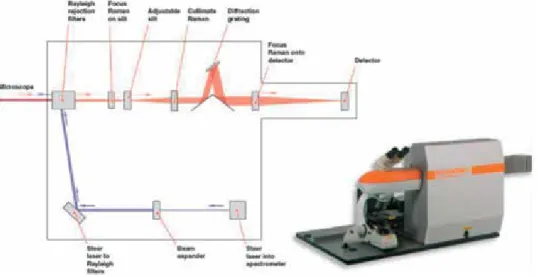
- Raman spectroscopy
- Grazing incidence X-ray diffraction (GIXD)
- Nanoscale mechanical properties
- Electrical transport and resistivity
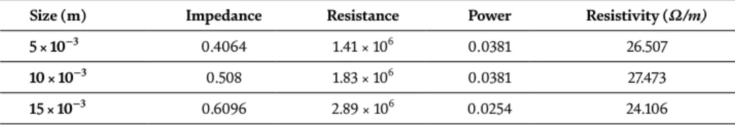
The observations show a high degree of porosity and vertically aligned MoS2 film matrix, as shown in Figure 2A-C which is consistent with Kong et al. The crystal structure was studied using electron microscopy techniques as described by Chianelli et al. Scanning electron images taken during the ablation procedure to prepare a needle for atom probe tomography in a MoS2 thin film (green square and circles are the areas of interest and cut using Ga ions and Omiprobe® micromanipulators.), as discussed by Szász et al. 3), having.
Razing incidence X-ray diffraction, it was possible to observe a dominant (101) reflection at 2θ ~30°, in agreement with Liu et al. 3). Razing incidence X-ray diffraction, it was possible to observe a dominant (101) reflectance at 2θ ~30°, in agreement with Liu et al.
Discussion and conclusion
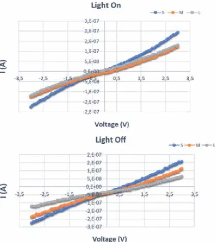
Resistance ρ values, calculated from I-V curves measured in the presence of white light and dark environment using four-point method over MoS2 film's surface. Above: I-V curves measured in the presence of white light and using four-point method MoS2 film. This chapter is distributed under the terms of the Creative Commons Attribution License (http://creativecommons.org/licenses/ . by/3.0), which permits unrestricted use, distribution, and reproduction in any medium, provided the original work is properly cited.
HRTEM and molecular modeling of the MoS2-Co9S8 interface: understanding the promotion effect in bulk HDS catalysts. Structural and textural properties of Fe2O3/γ-Al2O3 catalysts and their importance in the catalytic reforming of CH4 with H2S for hydrogen production.