Graphene is one of the most promising materials in the world and has attracted a lot of attention. Much research has been done to investigate the promising properties of the single-layer graphene sheets (SLGSs) after the appearance of the new method of graphene sheet preparation.
Mechanical properties
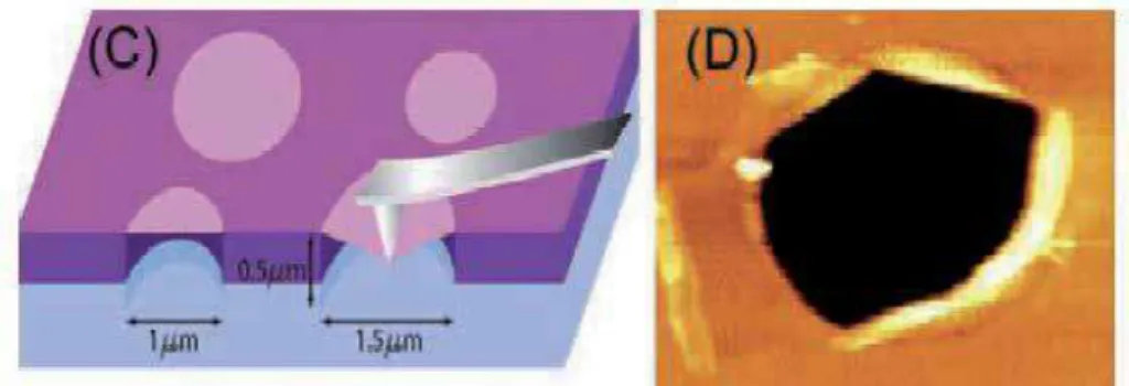
Under the simultaneous action of these problems, atomic bonds near a crack tip are broken and propagation takes place. Their simulation showed that with the low-strength adhesive, tearing occurs in the conqueror armchair direction of the hexagonal crystal lattice of graphene, and meanwhile, occasional direction change is rarely observed.
Thermal Properties
The direction of heat flow in two-dimensional graphene can be divided into in-plane and out-of-plane directions. As can be seen in Figure 3a, the thermal conductivity along the c axis of pyrolytic graphite is only ~6 W m-1 K-1 at room temperature.
Electrical Properties of Graphene
The electronic properties of graphene are one of the prominent matters that related experimental studies have addressed. The high electronic mobility of graphene allows the development of the quantum hall effect (an effect visible in conductor and semiconductor materials; when there are both electric and magnetic fields at the same time in a conductor or semiconductor material, an electric potential perpendicular to the magnetic field can arise, causing electric current perpendicular to the magnetic fields and high electromagnetic fields and high electromagnetic fields (F4). Novoselov, et al., 2005;.
![Figure 3. (a) Thermal conductivity κ as a function of temperature for representative data of suspended graphene [55], SiO 2 -supported graphene [64], ~20-nm-wide graphene nanoribbons (GNRs)[63], suspended single-walled CNTs (SWCNTs)[66], multi-wal](https://thumb-ap.123doks.com/thumbv2/1libvncom/9200755.0/16.765.117.657.480.723/thermal-conductivity-temperature-representative-suspended-supported-nanoribbons-suspended.webp)
Molecular Dynamics (MD) modeling
Lattice Mechanics
The most important equation that we use in this technique is the Lagrange equations of motion. In lattice mechanics, we limit our studies to associate cells, which may comprise multiple unit cells; this is the consequence of the principle I discussed above.
Multi scale boundary condition
To solve the above equation of motion, we need to use mathematics such as the Fourier transform or the Laplace transform. In other words, we might be able to solve one part of the problem with atomistic modeling and the other part with continuum; the multiscale method uses both simultaneously and then links them together.
Multi scale Modeling
- MAAD
- Coarse-Grained Molecular Dynamics (CGMD)
- Quasi-Continuum Method
- Coupled Atomistics And Discrete Dislocation (CADD)
The link between atomistic and continuum is obtained by using the Cauchy Born rule. One of the best assumptions in this approach is that defects within atomistic region are allowed to move through the atomistic/continuum boundary in the continuum modeled by discrete dislocation mechanics.
Bridging- Scale Modeling
Equations of motion
Using the bridge scale enables us to decompose the total kinetic energy into the sum of the coarse-scale kinetic energy plus the fine-scale kinetic energy. However, as we will discuss, since we will eliminate the fine scale from the coarse scale, q will be limited to the fine scale (not the entire domain), and so it is not possible to compute the coarse scale solution everywhere via direct projection of the MD displacements.
Removing fine- scale degree of freedom in coarse- scale region
This is the unwanted degree of freedom that lengthens the time spent solving the FE, so we need to eliminate the effects of fine scales that extend into the coarse-scale region. These forces arise from the initial conditions on the eliminated fine-scale degrees of freedom.
Author details
In any case, all these nc atoms are located in the MD region with linear or harmonic behavior. The impedance force fimp has become for us a device to cancel out all the tiny information that cannot be represented in the continuum. These terms represent thermally motivated displacements and forces acting on a reduced MD system with fine-scale degrees of freedom removed.
34; Molecular Dynamics Methodology for the Study of the Solvent Effects on a Concentrated Diels-Alder Reaction and the Separation of the Post-Reaction Mixture." Computers and Chemical Engineering S27-S33. 34; Raman Measurements of Thermal Transport in Suspended Single-Layer Graphene of Variable Sizes in Vacuum and Gaseous Environments." ACS nano.
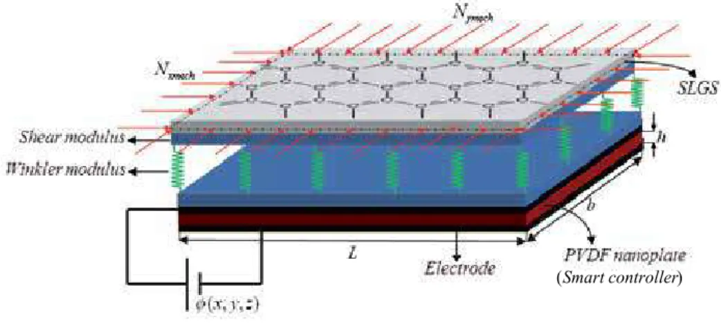
Modeling and Control of a Smart Single-Layer Graphene Sheet
Ghorbanpour Arani and F. Ebrahimi
- Introduction
- Review of nonlocal piezoelasticity and Mindlin plate theory
- Nonlocal piezoelasticity
- Mindlin plate theory
- Modeling of the problem
- Constitutive relations for PVDF nanoplate
- Constitutive relations for SLGS
- Solution procedure
- Numerical results
- Conclusion
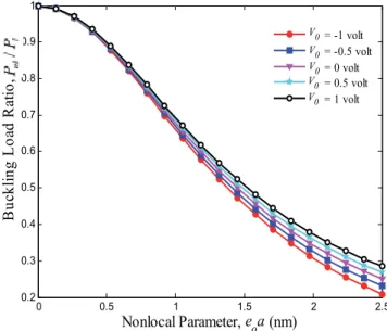
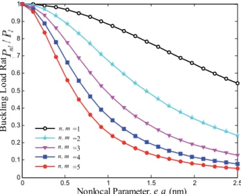
Figure 3 Effect of external stress on the deflection load ratio compared to the non-local parameter. 6 Effect of external stress on the ratio of deflection load to axial half-wave number. Effect of external stress on the ratio of deflection load to axial half-wave number.
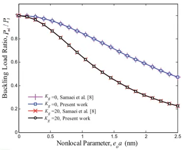
7 Effect of external stress on bending load ratio versus shear modulus parameter. Effect of external stress on bending load ratio versus shear modulus parameter.
Appendix A
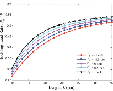
The governing equations are obtained based on the nonlocal Mindlin plate theory, so that the effects of the coefficient of the small-scale elastic medium, the number of modes, and the length of the graphene are discussed. The results show that the imposed external stress is an effective control parameter for SLGS bending. It was found that the effect of external stress becomes more pronounced at higher nonlocal parameters and shear modulus.
It is also observed that for a given length, the SLGS with a negative external stress will bend first compared to the SLGS with a positive one. Finally, we hope that the results presented in this paper will be helpful in the study and design of connected systems based on smart control and electromechanical systems.
Review of Graphene Technology and Its Applications for Electronic Devices
Graphene fabrication
- Exfoliation
- Carbon nanotube unzipping
- Sublimation and reconstruction from carbide
- Growth through condensation after carbide formation
- Epitaxial growth of graphene on a non-carbide forming catalyst
This rather crude method creates a random array of single- and double-layer graphene flakes on a desired substrate, which has been a key driver for research into many of graphene's properties. 21] This method has problems with the formation of defects due to shear stress and the reliable placement of graphene flakes after exfoliation. 33] There has also been some work using Ni and Cu bilayers to catalyze the production of graphene from SiC, achieving growth at higher pressures and lower temperatures.
The sublimation of graphene from SiC also creates a Si2O3 insulating underlayer that could aid in the transfer process. 31, 32] It is generally accepted that the production of graphene by surface absorption of carbon onto a non-carbide producing metal (such as Cu or Ir) is an epitaxial process due to the register between the underlying Cu (or Ir) crystal structure and the graphene layer.
![Figure 3. Diagram showing multiple mechanisms for inducing a band gap in graphene [19].](https://thumb-ap.123doks.com/thumbv2/1libvncom/9200755.0/68.765.106.668.125.532/figure-diagram-showing-multiple-mechanisms-inducing-band-graphene.webp)
Graphene doping
- Electrostatic doping
- Chemical doping
- Geometry restriction
43] Most electrostatic gates are achieved through a horizontal device architecture to preserve the mobility of graphene for ultra-fast devices. 19, 46] The chemical dopant mechanism of graphene works by ionically or covalently bonding the dopant to the delocalized pz orbital. The final way to anesthetize graphene is by breaking graphene's lattice periodicity, as shown in Figure 15.
19, 53] This can be done by reducing the size of a graphene sheet in one direction so that the Fermi levels of the periodic boundary conditions are refined, providing doping through a quantum confinement effect. 13, 53] This has been shown to be achieved by patterning graphene into one-dimensional ribbons.
![Figure 10. Diagram showing charge injection and Fermi modification of a graphene Schottky contact [43].](https://thumb-ap.123doks.com/thumbv2/1libvncom/9200755.0/73.765.273.490.117.231/figure-diagram-showing-injection-modification-graphene-schottky-contact.webp)
Graphene Field Effect Transistors (GFETs) and Radio Frequency (RF) electronics
- Short channel effects
- Metallic doping by source drain contacts in graphene
- Dielectric deposition and trap states
- FET design and gate coupling
- Graphene FET and RF electronic performance
To overcome some of the short channel problems and problems with graphene integration in ordinary process streams, a wafer binding type Integration has been proposed as shown in Figure 19. To demonstrate this is the amount of voltage reinforcement in such a graph-Fet drawn as a contour plot with the voltage reinforcing axis on the right side of the graph as shown in Figure 12, which shows a Threshold Frequarity, . The duct length of the graph-fet.
62] One group theoretically tuned all the parasitic capacitances that would limit the graphene channel mobility; this includes removing Schottky interactions at the source and drain contacts, removing any trapped states in the oxide, ignoring any electron/hole coupling effects, and perfectly matching the gate voltage to the channel potential, allowing a GFET operating at 1.5 THz. 62] By allowing the current to saturate the GFET, a voltage gain can be projected into the graphene channel; however, this would deteriorate the operating frequency of the GFET as shown in Figure 25.
![Figure 15. Different defined graphene sheet edge states and the associated band diagrams showing opening according to edge definitions [52].](https://thumb-ap.123doks.com/thumbv2/1libvncom/9200755.0/78.765.249.518.474.735/figure-different-defined-graphene-associated-diagrams-according-definitions.webp)
Graphene use in Electro-Optical (EO) devices
62] This GFET is optimized to have zero gain due to current saturation in the 50 nm channel. One of the interesting applications for graphene is its use in EO devices and lasers. 63–67] The problem with using graphene for pure optical devices is due to its inherent thinness that absorbs only 2.3% of incident light per layer.
63–67] This makes it more desirable to integrate graphene with other electro-optical components such as photonic cavities or a plasmonic waveguide with the example shown in Figure 26. 63] The modulator operated up to a frequency of 1.2 GHz, which was limited by the time constant of the RC capacitor.
Graphene Infrared (IR) detectors
Another group used an array of aligned graphene nanoribbons, as shown in Figure 27, to open up a small bandgap that has significant fabrication problems and noise properties of the nanoribbon edges. 45] Groups that have tried thermal IR detectors seem to have created more novelty, with one group using multiple vertically aligned graphene flakes, while another group used a resonant structure of two graphene sheets separated by a dielectric to tune the photon wavelength of absorption, as shown in Figure 28. Finally, another group used the photothermoelectric effect as shown in Figure 29 to induce an electric current in graphene due to electrical gates or dissimilarities similar metal contacts.
The resonance-based IR detector shown in Figure 28 uses the phonon resonance of two separate graphene sheets separated by a dielectric, allowing wavelength detection to be tuned based on the separation distance, but fabrication is difficult, requiring pristine graphene and no trapped states in the oxide that would both modify the resonant frequency and potentially contaminate the detector beyond its detection range. The photothermoelectric effect detector shown in Figure 29 is relatively straight forward, with contamination only affecting the velocity of the detector and the noise only being susceptible to confinement states of the insulating oxide onto which the graphene is transferred.
![Figure 27. The utilization of graphene nanoribbons to open a small band gap that is enhanced through the use of p- p-and n-type graphene contacts [45]](https://thumb-ap.123doks.com/thumbv2/1libvncom/9200755.0/85.765.249.514.303.745/figure-utilization-graphene-nanoribbons-small-enhanced-graphene-contacts.webp)
Conclusion
The use of graphene nanoribbons to open a small band gap that is enhanced by the use of p- and n-type graphene contacts [45]. It has been found that although the integration of graphene is challenging due to mobility degradation. The unique thermal-based properties of graphene either in a traditional bolometric type of device or one based on current produced from the photoelectric effect enabled the creation of a graphene IR detector with sensitivity to a 2.5 THz (119 µm) laser.
Han, Barbaros Özyilmaz, Yuanbo Zhang in Philip Kim, »Energy Band- Gap Engineering of Graphene Nanoribbons«, Physical Review Letters, številka 98, Arti. Vasko, “Electro-optics of graphene: Field-modulated refleksija in dvolomnost”, Physical Review B, Issue 81, Article Number.
From Functionalization to Applications
- What is photoactive graphene?
- Why photoactive graphene?
- Rational design of photoactive graphene
- Processability
- Energy level tuning
- Chemical functionalization
- Energy transfer and charge transfer
- Charge transfer
- Energy transfer
- Applications of photoactive graphene
- Organic Photovoltaic (OPV)
- Photocatalysts
- Conclusions and outlooks
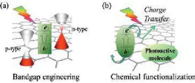
Recent research results have shown that chemical functionalization of graphene with photoactive moieties is a necessity to exploit its full potential.[8]. In addition, the functional molecules attached to the basal face of graphene lead to modification of the π–. The linear relationship between the absorbance and the concentrations of the graphene moiety in the composites indicates good dispersibility of the composite.
The π–π stacking interaction between the aromatic graphene backbone and conjugated planar molecules enables synergistic binding interactions. These measurement results provide quantitative insight, both kinetically and spectroscopically, into the nature of the interactions between graphene and photoactive molecules.
![Figure 3. (a) Thermal conductivity κ as a function of temperature for representative data of suspended graphene [55], SiO 2 -supported graphene [64], ~20-nm-wide graphene nanoribbons (GNRs)[63], suspended single-walled CNTs (SWCNTs)[66], multi-wal](https://thumb-ap.123doks.com/thumbv2/1libvncom/9200755.0/15.765.101.663.324.606/thermal-conductivity-temperature-representative-suspended-supported-nanoribbons-suspended.webp)
![Figure 3. Diagram showing multiple mechanisms for inducing a band gap in graphene [19].](https://thumb-ap.123doks.com/thumbv2/1libvncom/9200755.0/67.765.90.677.114.561/figure-diagram-showing-multiple-mechanisms-inducing-band-graphene.webp)
