Inquiries regarding the use of the book should be addressed to the Rights and Permissions Department of INTECHOPEN LIMITED ([email protected]). In particular, the change in optical properties in the nanometer has attracted the interest of the scientific community.
157 Surface Plasmon Enhanced Chemical Reactions on Metal Nanostructures
Introduction
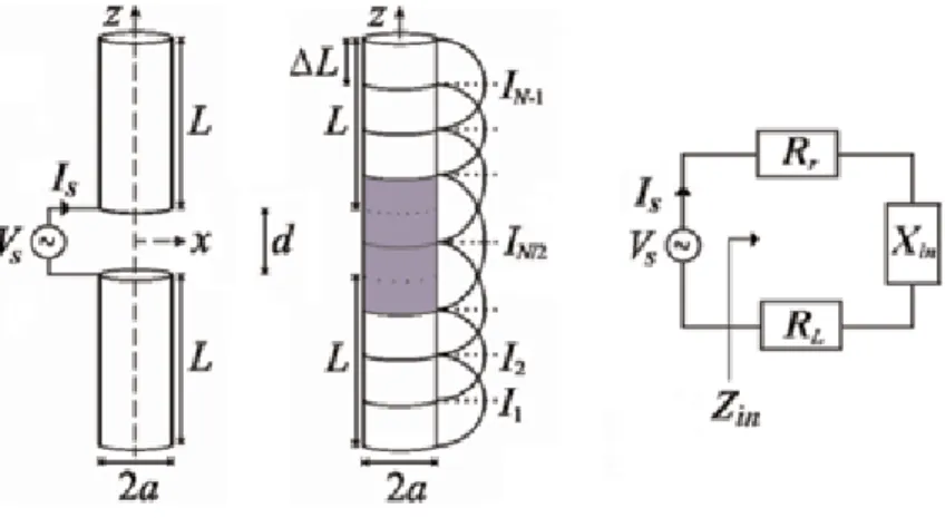
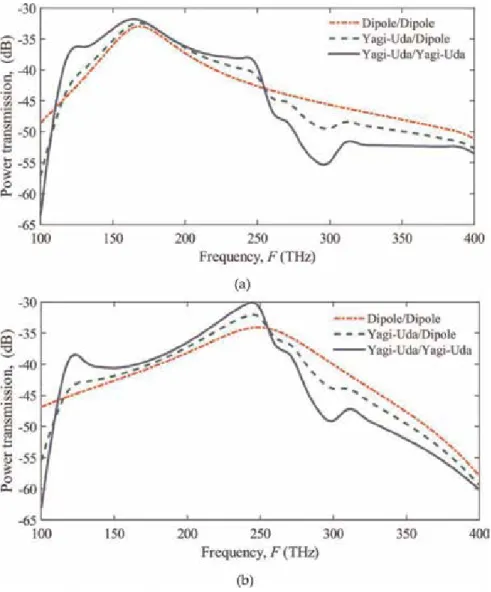
In this work, we present a theoretical analysis of wireless optical nanolinks formed by plasmonic nanoantennas, where the considered antennas are Yagi-Uda and cylindrical nanodipoles made of Au. In this analysis, the transmit power and the near electric field are investigated for three nanolinks: Yagi-Uda/dipole, Yagi-Uda/.
Description of nanolinks
The nanojunction is located in free space and is formed by cylindrical gold conductors. The receiver antenna is a dipole (Figure 1 right), located in the z = 0 plane and shifted to a dTR.
Numerical model
- Method of moments
- Finite element method
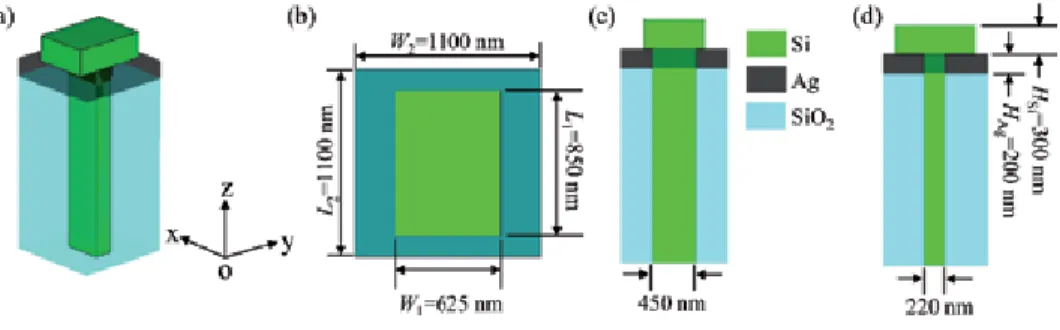
In this figure, L is the arm length, d is the nanodipole gap, and a is the dipole radius. The integral equation for the scattered field along the length l of the nanodipole is given by
Numerical results
- Isolated antennas in transmitting mode
- Nanolinks analysis
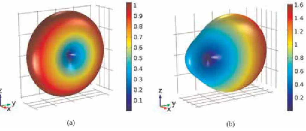
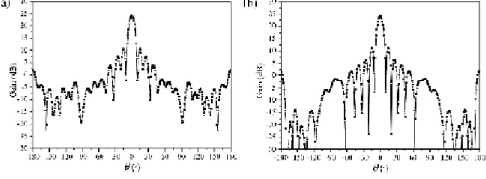
It is observed that the maximum gain of the Yagi-Uda (Gmax≈1.6) is approximately 60% greater than the maximum gain (Gmax≈1) of the dipole. For the case of the Yagi-Uda antenna, the maximum gain occurs in the +y direction with a small lobe in their direction.
Conclusions
Based on the light interference principle, beam steering is realized by controlling the phase of the light emitted by each nanoantenna in the optical antenna array. This kind of bottom-fed plasmonic nanoantenna is suitable for expanding the nanoantenna array.
Plasmonic nanoantenna
- Radiation characteristics of the designed plasmonic nanoantenna
- Parameter analysis of the plasmonic nanoantenna
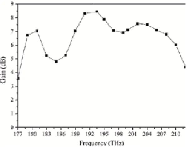
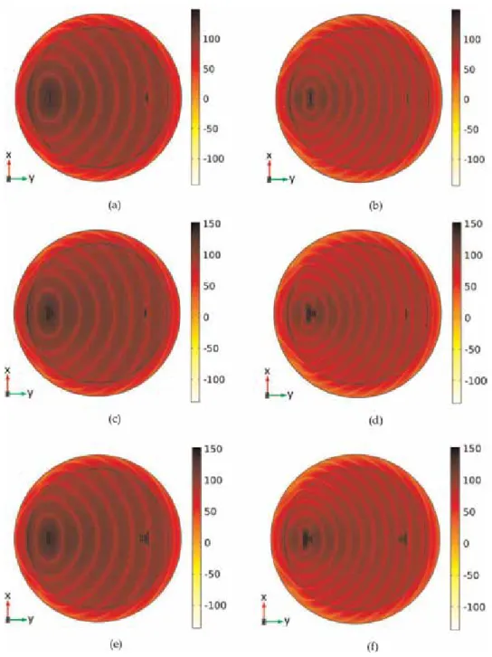
Simulated optical field in (a) x-o-y cross section and (b) x-o-z cross section of the designed plasmonic nanoantenna at 193.5 THz. The variation of gain with the length of the silver block (L2) increasing from 900 to 1300 nm is shown in Figure 7(b).
Plasmonic nanoantenna arrays
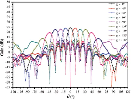
Finally, the influences of the heights of silicon block (HSi) and silver block (HAg) in the plasmonic nanoantenna structure on the gain are also analyzed, as shown in Figure 8 (a) and (b), respectively. 8 × 8 array structure with 0.7λ0 element spacing in x and y axis directions.
Conclusion
This chapter discusses different approaches for calculating the modified Mie-Lorenz coefficients of the graphene-based multilayer cylindrical and spherical geometries. In addition, the real and imaginary parts of the graphene equivalent bulk dielectric constant are shown in Figure 2(c) and (d).
Graphene-coated cylindrical tubes
- Scattering from graphene-coated wires
- Multilayered graphene-based cylindrical structures
In the above equation, Z is the solution of Bessel's differential equation and n is its order. The plasmon excitation frequency is the complex poles of the extracted coefficients [24], which will be discussed in the next subsection.
Graphene-coated spherical structures
- Multilayered graphene-based spherical structures
Later, the extracted modified Mie-Lorenz coefficients can be rewritten in the form of polynomials. Later, the extracted modified Mie-Lorenz coefficients can be rewritten in the form of polynomials.
Nanoplasmonics and quantum treatment of plasmons
- Basic principles
- Specific properties of surface plasmons
- Plasmon loss mechanisms
- Surface plasmons in quantum mechanical picture
Interaction of an electromagnetic field with surface plasma waves and generation of surface plasmon polariton waves. where "β" is the Landau nonlocal parameter that becomes important for large values of wavenumber. It can be concluded that in the "x" direction "ΔxΔα ≥2π" in which α is the x-component of the wave number.
Physical models for analyzing plasmonic nanolasers
- Plasmon cavity quantum electrodynamics (PCQED)
- Quantum mechanical atomic-scale model
- Mean-field atomic-scale model (optical Bloch)
- Semiclassical rate equations
One of the most fundamental differences between them is the enhancement of the spontaneous emission rate in a plasmonic cavity by the Purcell factor. In a homogeneous medium, the spontaneous emission rate "A" is equal to "1/τsp0" and "τsp0" is the spontaneous emission lifetime of the material.
Different structures of metallic nanoscale plasmon sources
In these equations, "n" is the excited-state carrier population, "s" is the number of plasmons in the lasing mode, and "Rp" is the carrier generation rate. Different structures of plasmonic nanolasers: (a) plane plasmonic nanolaser [13] (subwavelength in one dimension), (b) typical nanowire-based plasmonic nanolaser [16] (subwavelength in two dimensions), and (c) quantum cavity plasmonic laser [15] (subwavelength in three dimensions).
Proposed nanoresonator structures
Many of the semiconductors were typical optoelectronic materials (III-V and II-IV alloys) such as GaAs, AlGaAs, ZnS, InGaAs, InP, etc. [13]. By using the Finite Difference Time Domain (FDTD) mode analysis method and numerically solving nonlinear velocity equations of (37), the output performance of the proposed structures can be derived.
Conclusion
This book chapter provides more details for the development of these two simple methods and the discussion of the improved mechanism, which can be very useful for the next generation of photodetection. The diameters and spacing of Au NPs will affect the resonance wavelength and absorption of the device. ii).
- The preparation process
- The performance of the WS 2 -based photodetector
- The theoretical mechanism
The bandgap is approximately 1.96 eV, as shown in the inset. d) The AFM elevation profiles and associated AFM image of 1 L-WS2. Visible to NIR light response of the fabricated photodetector [22]. a) The drain-source current (IDS ) changes from −2 to 2 V due to the drain-source bias. The optical power is 20.5 mW/cm2 for these three wavelengths.
The preparation and theoretical mechanism of magnetron- sputtering-based MoS 2 photodetectors
- The preparation process
- The structure of the MoS 2 -based photodetector
- The performance of the MoS 2 -based photodetector
- The operational mechanism
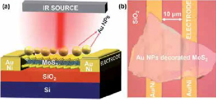
Raman shift of exfoliated bare MoS2 sheet and Au NPs decorated MoS2 with different (b) sputtering electric current (LPP1, HPP1). Figure 10a,b shows the cross section of the simulated electric field distribution of Au NPs decorated MoS2.
Optical trapping and optical tweezers
Although several research works in the literature have considered loss in plasmonics as detrimental, it is now known that loss in plasmonics can be beneficial for rapid on-chip manipulation of nanoparticles [ 17 , 20 ]. The loss-induced heating effect resulted in a growing thermoplasmonic metasurface field.
Plasmonic optical tweezers
The first challenge arises because the value of the gradient force is proportional to the third power of the particle radius in the quasi-static limit. The thermal gradient results in a gradient in the permeability and electrical conductivity of the fluid.
Electrothermoplasmonic, electro-osmotic and thermophoretic effects As mentioned in the previous section, the heating effect from plasmonic
When the temperature in the liquid is no longer uniform due to a thermal gradient, a gradient in the dielectric constant and conductivity of the liquid will also be induced. The direction of the DEP force is along the electric field intensity gradient and its sign depends on the sign of the Clausius-Mossoti factor.
Thermoplasmonic nanohole metasurface
Due to the plasmon response, the electromagnetic field is restricted near the edges of the nanohole and the region between the nanohole, as shown in Figure 2. Experimental images of trapped particles on the surface of the nanohole array are shown in Figure 5(b).
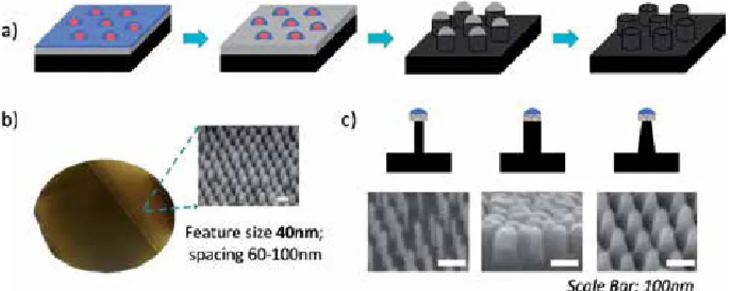
Spatially controlled fabrication of nanoscale templates 1 Fabrication of self-assembled templates
- Reproducibility and scalability
The distribution of the subsequent pattern on the surface can be varied in steps <5% of the mean value, through control of the evaporation rate or the concentration of the micelles in solution. Schematic representation of the self-assembly of amphiphilic di-block copolymer into reverse micelles and their subsequent assembly to form two-dimensional arrays on the surface.
Nanoplasmonic arrays by pattern transfer
- Nanoparticle cluster arrays
- Metal nanopillars arrays
- Nanorods and nanodisc arrays from nanoimprint lithography from self-assembly derived high-resolution masters
The low standard deviation of the template allows for a low standard deviation in the geometric attributes of the clusters as well (Figure 5). Separations between clusters are controlled by controlling the stencil height.
Conclusions and outlook
Using a ferrocenylsilane-based block copolymer as a template to produce nanotextured Ag surfaces: Uniformly enhanced surface enhanced Raman scattering of active substrates. Arrays of metal nanoparticles: A common substrate for both surface-enhanced Raman scattering and surface-enhanced infrared absorption.
Lembrikov, David Ianetz and Yossef Ben Ezra
Hydrodynamics of SmALC in the external electric field
In this section we briefly discuss the SmALC hydrodynamics and derive the equation of motion for the normal displacement of the smectic layer u x, y, z, tð Þ in the external electric field E!ðx, y, z, tÞ. 2ε0εikEiEk (7) Here K�10�11N is the Franke elastic constant related to the orientational energy SmALC within the layers, ε0 is the free space permittivity and εiki the SmALC permittivity tensor including the terms determined by the smectic layer stresses.
SPP modes in a MIM waveguide with SmALC core
The SmALC in the waveguide core is homeotropically oriented, i.e. the smectic layers are parallel to the waveguide cladding z¼ �d, while the elongated SmALC molecules are mainly parallel to the Z-axis [29]. The electric field of the counter-propagating SPP modes of type (26) in the MIM waveguide SmALC core has the shape.
Nonlinear interaction of SPPs in the MIM waveguide
Time dependence of SPP normalized intensities I1,2ð Þt for pump wave amplitude ESA10ð Þt. We evaluated the dynamic lattice displacement of the smectic layer augmented by perturbing SPPs.
Surface plasmon resonance effect on PMNMs and its fast relaxations The phenomenon of collective excitation of free electrons present in the noble
Effect of surface plasmon resonance in PMNM and its fast relaxations The phenomenon of collective excitation of free electrons present in the noble. A significant decrease in the lifetime of hot carriers was observed as the size of silver nanoparticles increased [20].
Photoinduced charge transfer of aromatic nitro and amino molecules on PMNMs
- Effect of pH toward photochemical reaction on PATP-adsorbed PMNMs In order to give a clear explanation of the effect of pH, adsorption of molecules
- Adsorption configurations of PATP on PMNMs
- Surface catalytic coupling reactions on PMNMs
But for DMAB, such a Raman spectrum for PATP adsorbed on silver cannot be obtained even considering the photon-driven charge transfer mechanism. Therefore, the directions of charge transfer are opposite for the low-lying excited states of PATP and DMAB.
Aerobic oxidation-assisted aromatic amine on PMNMs photocatalysts The mechanism for the electrochemical reduction of aromatic nitro compounds
In the absence of active oxygen species, the hot-hole oxidation mechanism for the conversion of PATP to DMAB is shown in Figure 8B. The presence of interfacial defects/small clusters prolongs the lifetime of hot electrons or holes on the surface of PMNMs. An apparent decrease in the lifetime of hot electrons and holes was observed as the continuous distribution of energy band seen around the Fermi level on the PMNMs [62].
Summary and prospects
The major concern for hot electrons can only be observed in the photochemical reactions on the surface of PMNMs. Charge-transfer resonance process in surface-enhanced Raman scattering of p-aminothiophenol adsorbed on silver - Herzberg-Teller contribution.
Novel two-dimensional materials beyond graphene
- Buckled honeycomb lattices
- Molybdenum disulfide and transition-metal dichalcogenides
As we will see below, all the individual electronic and collective properties of curved honeycombs depend on both band gaps Δ<,> and can therefore be tuned by changing the perpendicular electric field to create different types of functional electronic devices. A set of somewhat cumbersome analytical expressions for the components of the wave functions corresponding to the dispersions in Eq.
Thermal plasmons in graphene and other materials
For MoS2, its dispersions and DOS corresponding to the parabolic band approximation in Eq. 23), are also shown for comparison. The dielectric function introduced in equation 4) is directly determined by the finite temperature polarization function or polarizability, ΠTðq,ωjμð ÞT Þ, which is,.
Chemical potential at finite temperatures