Moreover, at the end of the chapter, different applications of these nanomaterials are explored. Much of the interest in nanotechnology is due to the fact that the nanoscale features are very different from the larger scale with which we are familiar. The first nanoscale observations were made in the first decade of the 20th century by Richard Adolf Zsigmondy.

APPLICATIONS
RECENT RESEARCH AND FUTURE PERSPECTIVES
Exploiting the full potential of nanotechnology requires a significant amount of research required in the fields of nanotechnology. The number of Science Citation Index (SCI) papers reflecting discoveries in the field of nanotechnology reached about 65,000 in 2008 compared to 18,000 in 2000, indicating the rapid increase in popularity and interest in nanotechnology. The 2007 cost of the medical system in the United States consists of $90 billion spent on cancer treatment.

CONCLUSIONS
GENERIC METHODOLOGIES
INTRODUCTION
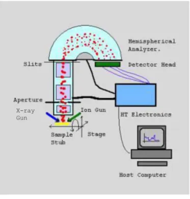
SCANNING PROBES
- SCANNING TUNNELING MICROSCOPY
- ATOMIC FORCE MICROSCOPY
- MAGNETIC FORCE MICROSCOPY
Microscopes have always been one of the essential instruments for research in the biomedical field. Comparison of STM topographies of a graphene wrinkle and a "flat" part of the same graphene sheet. An image of the magnetic stray field is obtained by slowly scanning the cantilever over the sample surface in a raster-like manner.

ELECTRON MICROSCOPY
- SCANNING ELECTRON MICROSCOPY
- TRANSMISSION ELECTRON MICROSCOPY
An electron gun, located at the top of the column, produces electrons and accelerates them to an energy level of 0.1–30 keV. This process reduces the size of the electron source (~50 μm for a tungsten filament) to the final required spot size (1–100 nm). The image contrast was reversibly switched when switching back and forth between 1 and 5 kV, indicating a contrast dependence of the SAM on the operating voltage of the SEM.
DIFFRACTION TECHNIQUES .1 X-RAY DIFFRACTION
A technique based on HCDF-TEM to examine the dislocation structure was presented and then applied to examine the dislocation density in trimodal Al MMCs containing nanocrystalline (NC-Al) and coarse-grained (CG-Al) AA5083 Al alloy. It was measured that the density of dislocations in the CG-Al phase is relatively small, 4 × 10¹⁴ m−2, even after hot expansion ratio (HSR) extrusion. The authors have successfully conducted an investigation where they indicate that the CG-Al phase can significantly increase the ductility of trimodal Al MMCs.
SPECTROSCOPY TECHNIQUES
- FOURIER TRANSFORM INFRARED SPECTROSCOPY
The FTIR spectrometer gives the most accurate and precise result in the infrared spectrum compared to other methods. It has a single beam splitter in the middle that splits the light source into two equal parts. After exiting the interferometer, the beam is focused through the sample in the sample compartment.
SURFACE ANALYSIS AND DEPTH PROFILING .1 AUGER ELECTRON SPECTROSCOPY
- SECONDARY ION MASS SPECTROSCOPY
When the ion hits the surface of the material, its charge and kinetic energy are transferred to the surface molecules in contact. As the outer layer of the sample slowly wears away, depth profiling enables a continuous, layer-by-layer analysis of its surfaces. In addition, the area analyzed on the sample is dependent on the size of the ion beam.
CONCLUSIONS
With this beam, more complex molecules will be able to detach from the surface. This modification has already boosted SIMS research in the biological field, because scientists are able to study the surface of the material without reducing it to simple carbons. Spectroscopy techniques such as FTIR allow us to analyze the composition of materials at the nanoscale quickly without damaging the sample itself, while the SIMS technique is able to demonstrate 3D profiling of the material.
SMART NANOMATERIALS *
CHAPTER 3
- INTRODUCTION
- NANOSCALE MATERIALS .1 HYDROGELS
- POLYMER BRUSHES
- CARBON NANOTUBES
- CELLULOSE
- MECHANISMS OF RESPONSE
- pH-RESPONSIVE NANOMATERIALS
- LIGHT-RESPONSIVE NANOMATERIALS
- TEMPERATURE-RESPONSIVE NANOMATERIALS
- MAGNETIC FIELD RESPONSIVE NANOMATERIALS
- BIOLOGICAL AND CHEMICAL RESPONSIVE NANOMATERIALS
- SYNTHESIS
- COACERVATION/PRECIPITATION
- LAYER-BY-LAYER POLYMERIC SHELL
- GRAFTING ONTO THE SURFACE OF PARTICLES
- HETEROGENEOUS POLYMERIZATION
- APPLICATIONS
- ENTRAPPING ABILITY AS NANOCARRIERS
- BIOLOGICAL POTENTIAL
- FIELD-EFFECT TRANSISTORS
- FIELD EMISSION DISPLAYS
- CURRENT RESEARCH AND FUTURE PERSPECTIVES
- CONCLUSIONS
Changing the pH of the solution shifts the chemical equilibrium and changes the degree of ionization (charging neutral particles) of the polymer chains (Ruhe et al., 2004). This increase in heat will result in the swelling of the polymer shells, which is an ideal change in drug delivery applications. One of the emerging applications of smart nanomaterials is the development of smart nanotextiles.

NANOSENSORS *
CHAPTER 4
- INTRODUCTION
- MANUFACTURING METHODS
- TOP–DOWN LITHOGRAPHY
- BOTTOM–UP ASSEMBLY
- MOLECULAR SELF-ASSEMBLY
- TYPES OF NANOSENSORS .1 CHEMICAL NANOSENSORS
- NANOBIOSENSORS
- NANOSCALE ELECTROMETERS
- DEPLOYABLE NANOSENSORS
- MULTIANALYTE SENSOR ARRAYS
- NANOSTRUCTURES AND MATERIALS .1 NANOWIRES
- CARBON NANOTUBES
- THIN FILMS
- NANOPARTICLES
- POROUS SILICON
- APPLICATIONS .1 MEDICINE
- SECURITY
- ENVIRONMENTAL
- INDUSTRIAL
- CURRENT RESEARCH AND FUTURE PERSPECTIVES
- CONCLUSIONS
In the top-down approach, highly ordered nanolines can be obtained via various lithography methods such as electron beam lithography or nanoimprint lithography. By means of molecular self-assembly, the desired structure is programmed into the shape and functional groups of the molecules. The nanotube's conductive properties change when chemicals in the surrounding environment bind to the tube.
Nanowires exhibit a change in conductivity in response to variations in the potential or electric field at the surface of the FET (Patololsky, 2006). LSPR spectra are extremely sensitive to these changes in refractive index, and the resulting shift in LSPR spectra can be used to detect molecules. By adjusting the size of semiconductor QDs, arbitrary fluorescence colors in the visible spectrum can be obtained.
The resistance then produced is correlated with the amount of gas present in the human breath (Gouma, 2010) (Stanacevic, 2004). This knowledge can be used to accurately and quickly treat any threats or diseases present nearby. Aguilar (2010) describes a nanosensor capable of detecting trace amounts of various explosives, including TNT, in the presence of interferents.
The sensors are reversible because the components are hydrophobic and remain in the sensor core.

NANOPARTICLES *
CHAPTER 5
- INTRODUCTION
- SYNTHESIS AND CHARACTERISTICS
- MAGNETIC NANOPARTICLES
- METAL NANOPARTICLES .1 Synthesis methods
- POLYMER NANOPARTICLES FOR SEMICONDUCTORS
- APPLICATIONS
- APPLICATION OF MAGNETIC NANOPARTICLES
- APPLICATION OF METALLIC NANOPARTICLES
- APPLICATION OF POLYMER NANOPARTICLES
- CURRENT RESEARCH AND FUTURE PERSPECTIVES
- CONCLUSIONS
One of the many methods is the polyol method that does not use metal bodies. Concentration of precursors (arbitrary units) InjectionNucleation Growth from solution. A) Monodisperse colloidal growth concept of the La Mer model, (B) typical synthetic apparatus. In order to achieve dispersion, "the entropic penalty associated with nanoparticle addition must be balanced by favorable enthalpy interactions" (Polymer-Nanoparticle Composites Part 1 (Nanotechnology), 2010).
Also, for separation applications, it can be used in optical sensing, due to the high sensitivity of magnetic nanoparticles. Due to the guide of the magnet, it can be delivered to the specific site and then the medicine is released. It then releases the drug due to a change in the internal environment (such as pH).
The integration of nanoparticles into polymers is one of the most significant theoretical and experimental interests in the polymer and engineering communities. 2003) reviewed some of the physical properties of magnetic nanoparticles and described some of their biomedical applications. In addition to looking at the applications of magnetic nanoparticles, much research is dedicated to the actual preparation of the particles.
For this reason, isotopic substitution was used to verify "the frequency assignment and the results conclusively demonstrate that the impurities originate from precursors." An isochronous annealing experiment was also performed to study the formation and stability of CO2 molecules.

NANOPOLYMERS *
CHAPTER 6
- NANOPOLYMERS AND THEIR APPLICATIONS
- FABRICATING NANOPOLYMERS: ELECTROSPINNING
- ENVIRONMENTAL APPLICATIONS
- FUEL CELLS .1 Introduction
- HEAVY METAL ION REMOVAL .1 Introduction
- SOLAR ENERGY .1 Introduction
- BIOMEDICAL TECHNOLOGY
- WOUND HEALING
- BIOMATERIALS
- POLYMERIC NANOFIBERS AS SENSORS
- CLASSIFICATION OF POLYMERIC NANOFIBERS
- HOW A POLYMERIC NANOFIBER SENSOR WORKS
- FABRICATION OF NANOPOLYMERIC SENSORS
- TYPES OF SENSORS
- CONCLUSIONS
Solar cells are made from the same type of semiconductor materials, such as silicon, that are used in the microelectronics industry. If it is close to the surface of the epithelium, it will gradually be pushed out of the host. If the mechanical strength of the scaffold can be increased, the nanofiber can be practically used for bone regeneration.
It was found that the higher the fibrinogen content in the composite, the smaller the water contact and the smaller the fiber diameter of the nanofiber. This current is measured and correlated to the concentration of the particular compound being measured. The method of doping can include many processes depending on the shape of the polymeric base.
Polymeric nanosensors can be used in many applications related to any of the above, which can include almost anything tangible. All the conducting materials used in the following experiments exhibit some molecular polarity. The greater slope above shows the greater sensitivity of the nanopolymeric sensor compared to film sensors.
Results for PEO/LiclO4 humidity sensor compared to the film sensor. a) the results for the PEO/LiclO4 sensor and (b) the film sensor.

NANOTUBES *
CHAPTER 7
- INTRODUCTION
- HISTORY
- CLASSIFICATION OF CNTs
- MOLECULAR STRUCTURE
- STRUCTURES OF SWCNTs
- PROPERTIES
- MECHANICAL PROPERTIES
- ELECTRICAL PROPERTIES
- THERMAL PROPERTIES
- PRODUCTION METHODS OF NTs
- ARC DISCHARGE METHOD
- LASER ABLATION METHOD
- CVD METHOD
- PURIFICATION OF NTs
- AIR OXIDATION
- ACID REFLUXING
- SURFACTANT-AIDED SONICATION, FILTRATION, AND ANNEALING
- APPLICATIONS OF CNTs
- EXISTING APPLICATIONS .1 CNT composites
- POTENTIAL AND UNDER DEVELOPMENT APPLICATIONS .1 Body armor
- CURRENT RESEARCH AND FUTURE PERSPECTIVES
This strength is a result of the sp2 covalent bonds created between the individual carbon atoms. Functionalization of the tubes and use of surfactants in combination with sonication are some of the methods developed. Carbon nanotubes – the path towards applications. critical on the NT tip structure: increased emission results from opening of NT tips. stone and molybdenum tip arrays, NT field-emitting surfaces are easier to fabricate and require less vacuum for operation.
Production of the NTs in the reaction chamber results in the formation of a smoke-like superelastic material. Due to special alignment of NTs arrays, they can be drawn into sheets at speeds of up to 2 m/s. In addition, the irradiance intensity of the NT filament is much stronger than that of.
The inner layer of the antenna contains NTs with a lower bandgap compared to that of the outer layer. The NT speakers can be stretched up to twice their original size with little change in sound intensity (Xiao, 2008). Due to the transparency and high flexibility of NT sheets, they can be placed almost anywhere.
Applying an electric current to the NT films results in the generation of heat, which causes the surrounding air to expand and sound waves are generated.

NANOSHELLS *
CHAPTER 8
- INTRODUCTION .1 NANOTECHNOLOGY
- NANOSHELLS
- TYPES OF NANOSHELLS
- OXIDE NANOSHELLS
- METAL NANOSHELLS
- PROPERTIES OF NANOSHELL PARTICLES
- OPTICAL PROPERTIES
- LUMINESCENCE PROPERTIES
- THERMAL PROPERTIES
- SURFACE CHEMICAL AND CATALYTIC PROPERTIES
- MAGNETIC PROPERTIES
- APPLICATIONS OF NANOSHELLS
- PROTECTIVE WATERPROOF COATINGS FOR WOOD, METAL, AND STONE
- ION-SELECTIVE FILMS
- GOLD NANOSHELLS FOR BLOOD IMMUNOASSAY AND CANCER DETECTION AND THERAPY
- CURRENT RESEARCH AND FUTURE PERSPECTIVES
In the case of metal nanoshells, such as silica-shelled gold, the thickness of the shell can be up to about 20 nm. Nanoshells can be obtained in several ways, depending on the size and intended use of the nanoshell. The optical properties and absorption of gold nanoshells can be changed based on the thickness of the gold layer on silica core particles.
By changing the thickness of the shell by a small value, the color of the core-shell particles can be adjusted from one color to another. By changing the thickness of the shell, the variation in melting point can be observed. Complete deformation of the shell can be observed when silica-gold nanoshell particles are heated.
It is also non-magnetic and therefore does not affect the magnetic properties of nuclear particles. The optical properties of the nanoshells can be tailored so that they can be used for imaging and therapy. Selective nanoshell accumulation can be used for tumor imaging using the high permeability and retention properties of cancer cells (Pradeep, 2009).
This shows that the gold nanoshells appear at lower energies than nanospheres of the same diameter.

ELECTRONIC AND ELECTRO-
OPTIC NANOTECHNOLOGY * CHAPTER 9
- HISTORY
- THEORY OF ELECTRONIC NANOTECHNOLOGY .1 EFFECT OF SIZE ON METALS
- QUANTUM NANOSTRUCTURES
- THEORY OF ELECTRO-OPTIC NANOTECHNOLOGY
- ABSORPTION AND EMISSION TRENDS
- DISPLAYS
- POLYMER-DISPERSED LIQUID CRYSTALS
- DENDRIMERS
- MODULATORS
- PHOTODETECTORS
- ELECTROPHORETIC DISPLAY SYSTEMS
- SWITCHES
- PHOTONIC CRYSTALS
- MULTIPLEXERS
- CURRENT RESEARCH AND FUTURE PERSPECTIVES
One of the first applications found was their ability to emit very specific wavelengths of light. This effectively encompasses some of the challenges in electro-optical nanotechnology, including those presented in the literature review. It has been observed that as the particle size decreases, there is a shift in the absorption spectra to the blue (Poole & Owens, 2003).
The natural state of a smart window appears opaque due to the random orientations of the liquid crystals in the polymer. Nanoscale electro-optic modulators will be an integral part of a nanoscale communication network (Vlasov, Green, & Xia, 2008). There is no doubt that the field of electro-optical nanotechnology is one of the most valued areas in nanotechnology because its applications are almost limitless ranging from detectors to device displays.
Quadratic electro-optical effect is a change in the refractive index of a material in response to an applied electric field. Quadratic electro-optical effect in a nano-optical material based on the non-conjugated conductive polymer, poly(ethylenepyrrolediyl) derivative. Metal (gold) electrodes with a slit were deposited on the glass slide by evaporation prior to deposition of the PEP thin film.
Oscilloscope tracing of the modulation signal (peak waveform) in quadratic electro-optical measurement of doped PEP.


