The theory of an exciton formed by an electron and a spatially separated hole is developed in the framework of the modified effective mass method. A review devoted to the theory of excitonic quasimolecules (biexcitons) (consisting of spatially separated electrons and holes) in a nanosystem consisting of ZnSe quantum dots synthesized in a borosilicate glass matrix is developed within the context of the modified effective mass approximation.
Introduction
Spectroscopy of excitons in Quasi - Zero - Dimensional nanosystems
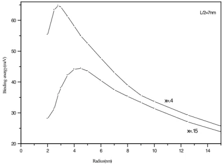
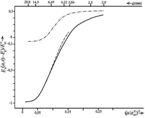
Therefore, the exciton ground state binding energies Eex(a, ε) (21) differ slightly from the corresponding total exciton ground state energies E0(a, ε) (17). The satisfaction of condition (23) likely makes it possible to neglect the effect of the complex QD valence band structure on the total energy (17) and binding energy (21) of the exciton ground state in the nano-.
Excitonic quasimolecules formed from spatially separated electrons and holes
The biggest contribution to the exchange is the interaction energy, which is created by the exchange energy of the interaction of the electron е(1) with the holes h (B), as well as the electron е(2) with the holes h (B) and the electron е(2) with the holes h (A). As a result, the average energy of the Coulomb interaction and the average energy of the exchange interaction of electrons е(1) and е(2) with holes h (A) and h (B) are greatly reduced compared to the binding energy of the exciton Eex(a), which results in the biexciton decay in the nanosystem into two excitons (formed from spatially separated electrons and holes) localized above the surface of QD(A) and QD(B) s.
Theory of new superatoms — Analogue atoms from the group of alkali metals
A large shift of the conduction band (about 400 meV) is a potential barrier for electrons (electrons move in the matrix and do not penetrate the volume QD). The polarization interaction energy of the electron and hole with a spherical surface section (QD matrix) provides a much smaller contribution to the potential energy of the Hamiltonian, and therefore contributions to a first approximation can be neglected [20–22].
Conclusions
Position of energy levels of the valence electron in some alkali metal atoms (K, Rb, Sc) and a new artificial atom, X. Level shifts of the valence electron (ΔERbк, ΔEScRb, ΔExSc) are relative to the adjacent level.
Author details
Thus, we propose a new model of an artificial atom, which is a quasi-atomic heterostructure consisting of a spherical QD (core superatom) with radius a and which contains zinc selenide in its scope surrounded by a matrix of borosilicate glass (in the volume of the QD, the effective mass of the hole mh, e and the effective mass of the electron me(1) is located in the matrix), and which is allowed to find a new artificial atom X (not in the periodic table of Mendeleev), which is similar to a new individual to an alkali metal atom.
Binding energy of the exciton of a spatially separated electron and hole in quasi-zero-dimensional semiconductor nanosystems. Theory of excitons formed from spatially separated electrons and holes in quasi-zero-dimensional semiconductor nanosystems.
Excitons and Trions
- Theoretical model
- Exciton
- Negative trion
- Positive trion
- Results and discussion
- Conclusion
- Appendix
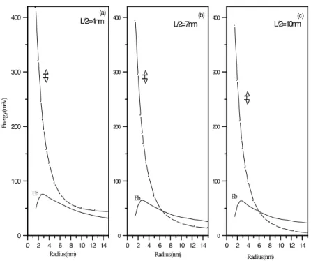
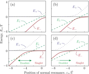
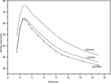
Crossing the binding energy curve with the Hamiltonian curve confirms our discussion above. We calculated the negatively charged exciton binding energy (E-b solid squares) and the positively charged exciton binding energy (E+b solid circles) as a function of the QD half-height.
On the ’Three-Orders Time-Limit’ for Phase Decoherence in Quantum Dots
Limitations on the quantum processing of information
To find another method of quantum error correction (despite great efforts there is still no relevant solution). In the case of quantum cryptography, equipment requirements [18] are more easily met with respect to decoherence and this is why this quantum technology (public key distribution via a quantum channel) has been used in practice in optical systems [fiber optic over distances of 100 km (up to 1000 km), and outside over distances of 2 km].
Quantum dots—the prospective technology for quantum gates
In nanotechnological and optical projects involving quantum computers (multi-qubit), the difference in the time speed of quantum operations compared to decoherence still does not exceed three orders of magnitude. 4 ensure that the time speed for the execution of logical operations must be at least six orders of magnitude faster than the decoherence time speed.
Phase decoherence of orbital degrees of freedom in nanostructures
- Phonon-induced dephasing of excitons localized in quantum dots
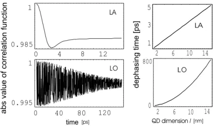
Through this technique, the correlation function of the exciton (electron) in the QD can be expressed, which defines the overlap (the scalar product) of the state of the carrier gradually dressed by phonons with the initial state of the bare exciton (or electron) in the dot. The excess energy of the lattice distortion (for acoustic phonons) along with the polarization energy (for optical phonons) is carried outside the QD by the LA and LO phonons (by their wave packets), respectively.
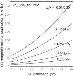
The universal rule for the estimation of the dephasing time of localized excitons in nanostructures
Modulus of the correlation function|a(t)a+(0)|(the fidelity measure of the ground excitonic state) versus time for increasing temperatures. Left: the modulus of the correlation function for LA (upper) and LO (lower) phonons, respectively.
Decoherence of the degrees of freedom of spin in quantum dots
- Dephasing induced by the dressing of QD exciton spin with magnons in a diluted magnetic semiconductor’s surroundings
- Spin waves in the diluted magnetic semiconductor
- Dressing of the QD’s local exciton spin by magnons from the surrounding DMS
- Explicit form of the interaction of magnons with QD spin causing the spin pure dephasing
A more detailed analysis of the problem (as will be presented below) shows that spin waves cause harmful decoherence within time velocities on the order of 500-1000 ps, which is a serious negative side effect that threatens the feasibility of the spin logic gate (again, in the middle of the six-order time window between the control time and the amplitude decoherence for spins [54]). The above formula (35) allows the calculation of the correlation function I(t) and the estimation of the spin dephasing time.
Magnon-induced versus phonon-induced QD exciton dephasing
It should be emphasized that due to spin conservation in the vertex, the two magnons must participate simultaneously in the interaction responsible for the dressing of the exciton state with the magnon cloud (i.e. this interaction part which causes the pure dephasing of the exciton spin). These factors tend to zero with decreasing temperature and completely freeze the pure dephasing of the exciton spin at T = 0 (in contrast to the charge dephasing process of phonons, which is kept strong even at T = 0—this is due to the emission factor 1+n(k) → 1 for T → 0, limit with 0 angle with phonon., low temperature, non-i.ex.
Conclusions
This difference is caused by the compatibility of the energy scale for carriers trapped in QDs with the band-phonon energy scale. Dressing the electrons/holes/excitons in QDs with bandphonons from the surrounding crystal induces the dephasing of charge (orbital degrees of freedom) in QDs (the off-diagonal decoherence).
Charge States in Andreev Quantum Dots
The origin of the fractional charge
To form a hole, the electron in the |k state attracts an electron in the |−k state and transfers to the superconductor forming a Cooper pair. The resulting state in a normal region maintains the electron-hole symmetry and thus carries an integer, if measured in the electron charge units, charge (we ignore hereafter a slight violation of the electron-hole symmetry of the order of ∆/EF arising as a result of finiteness of the Fermi energy).
A single Andreev level
Let us denote the position of the nth resonance relative to the Fermi level EF as εD = En+eVg−EF. Let us denote the position of the nth resonance relative to the Fermi level EF asεD = En+eVg−EF.
The charge of the Andreev quantum dot
The charge of the state |ν can also be found by differentiating the energy of this stateεν. The charge of the state|ν can also be found by differentiating the energy of this state εν.
Quantum fluctuations of the charge
Charge fluctuations due to electron-phonon interaction
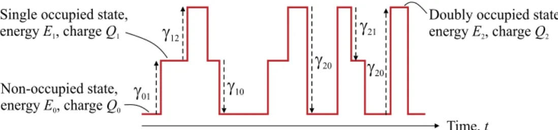
We see that the charge of the singly filled state (which has an integer charge) does not fluctuate, while the charges of the ground state and the doubly excited state (which has a fractional charge) fluctuate quite a lot. Transitions 0↔1 occur via emission of the extra quasiparticle with the energy belonging to the continuous spectrum, E>∆.
Fluctuations of the gate potential
One sees that the process 0 ↔ 2 is more frequent than the process 0 ↔1, since the latter includes the exponential factor exp(−∆/T), which enables reduction of the frequency γ01, by lowering the temperature, see Fig. belongs to the continuous spectrum which is accompanied by absorption of the phonon and decay of the Cooper pair. One sees that the process 0 ↔ 2 is more frequent than the process 0↔ 1, since the latter includes the exponential factor exp(−∆/T), which allows reduction of the frequency γ01 by lowering the temperature, see Fig.
Coulomb interaction
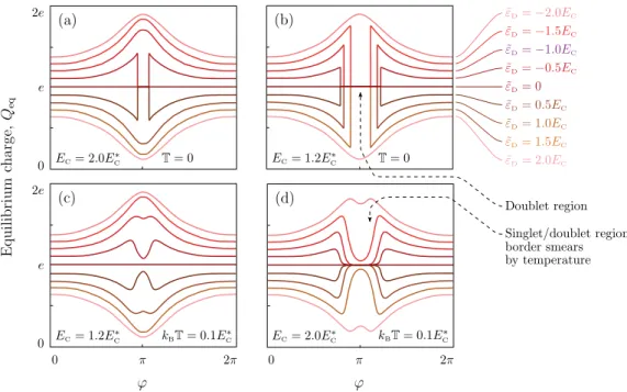
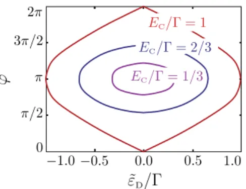
The doublet region in the coordinates (ϕ, ˜εD), where ˜εD =εD+2EC is the position of the normal resonance shifted by the Coulomb interaction. Everywhere except in the doublet region, the charge of the ground state is equal to Q−, while the charge in the doublet region is Q1=e.
Scaling of the charge
- Model rectangular potential
- Parabolic potential
- Graphene stripe with linear dispersion
In the case of a multi-walled nanotube (or normal metal) there may be more than one channel. Now, the phase-sensitive part of the contact-hybridized charge Q(ϕ,µ) can be calculated by summing over all channels.
Measuring of the fractional charge
Both are proportional to the width of the contact W, but in the case of SNS contact the factor does not depend on µ. However, the 0↔2 process can occur too quickly, at frequencies that exceed the resolution of the single-electron transistors.
Measurement of the flux by the Andreev quantum dot
The Andreev quantum dot charge can be measured with a sensitive magnetometer, for example, with a one-electron transistor. Nanomechanical effects can also suppress or enhance the Andreev quantum dot sensitivity with respect to the phase difference [49].
Conclusions
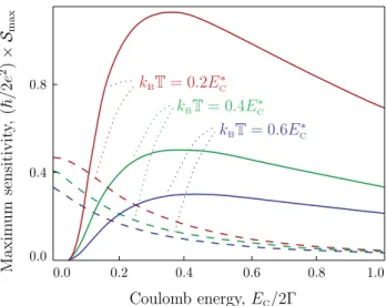
The 3EC∗ doublet region partially absorbs the I interval and the maximum at zero temperature is reached at the boundary of the doublet region. In the limit of small Coulomb interaction, the sensitivity is determined by the asymmetry of the quantum dot.
Applications
Quantum Dots Prepared by Droplet Epitaxial Method
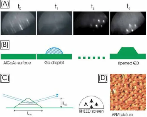
The droplet epitaxial technique
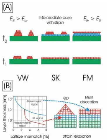
- Technological background and preliminaries of the droplet epitaxial technique It is well known in our profession that the grown structure can be classified in three growth
- Principles of DE
- QD engineering
The deformation takes place by adapting the uniform layer to the grid of the substrate. In the case of the DE, the surface clustering is done using the Volmer-Weber-like growth mode.
Droplet formation
- The initial surface status
- Size and density of the droplets
- Droplet–surface interaction
Here we discuss the dependence of the droplet shape and the so-called thermal etching. At the interface, the metal components of the substrate mix with the Ga atoms in the droplet.
Formation of QD
- Preparation technology
- Geometry and electronic structure of QD
- Some aspects to the kinetics of QD growth
Thus, the surface process is dominant during the processing time of QD production. The crystallization seed grows partly upwards and also partly in the direction of the drop inside.
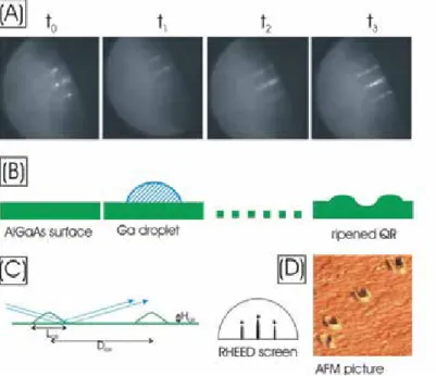
Ringlike QD preparation
- Growth technology of ringlike QD
- Geometry and electronic structure of the ringlike QD
- Some aspects to the formation of ringlike nanostructure
The initial phase of the surfaces is the same as in the case of conventional QD. It is known that the melting point decreases with decreasing particle size.
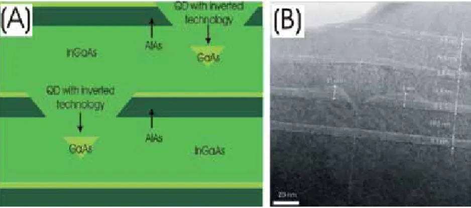
Specular-shaped QDs and complexes
- The inverted QDs
- The laterally aligned QD pairs
- Configuration of QD ensembles
The schematic and TEM image of the inverted QD structure is shown in Figure 11. In addition, the TEM image shows a thickening of the AlAs layer in the surrounding nanohole.
Acknowledgements
In the first case, the micro-PL spectra of a single QD pair show the ensemble of emissions, which may indicate the existence of a tunnel coupling between the members of the pair. During the preparation of the QD molecule, the height of the GaAs mound decreases from the original value and also the diameter decreases.
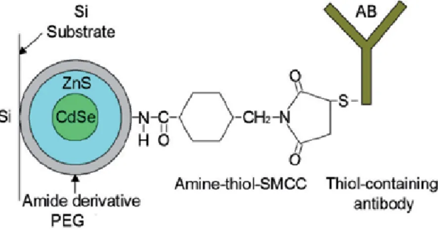
Antibodies
Physical Reasons for Differing Emission in CdSe/ZnS and CdSeTe/ZnS Quantum Dots in Bioconjugation in CdSeTe/ZnS Quantum Dots in Bioconjugation at.
Torchynska
QD bioconjugation process and experimental details
Raman scattering spectra were measured at 300 K using the Lab-Raman HR800 Horiba Jovin-Yvon spectrometer. Raman scattering spectra were measured at 300 K using the Lab-Raman HR800 Horiba Jovin-Yvon spectrometer.
The bioconjugation study of CdSe/ZnS QDs
- CdSe/ZnS QDs bioconjugated to HPV E7 and PRV Ab
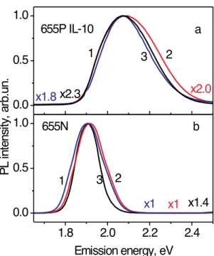
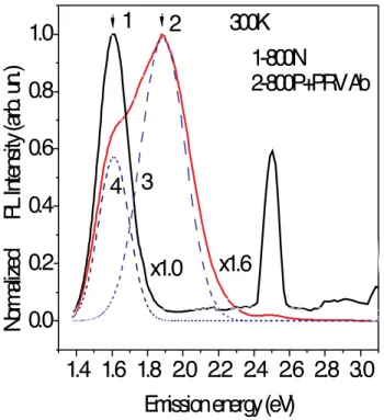
The PL spectra of 655N QDs kept a Gaussian shape of PL band (1.90 eV) at all excitation intensities. At the same time, the intensity of PL band related to the antibodies was 10-fold smaller than the PL intensity of CdSe/ZnS QD emission upon the UV excitation.
Discussion of the CdSe/ZnS QD bioconjugation
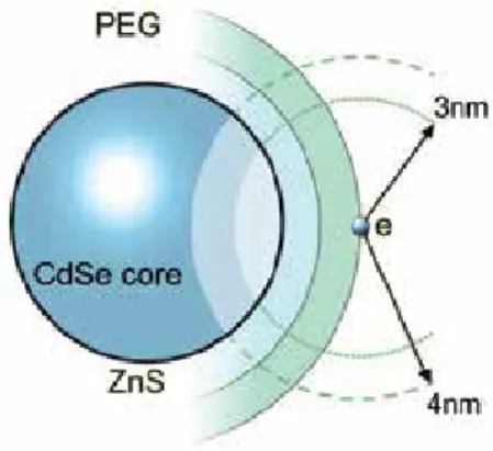
Another reason for the “blue” shift of PL peak in bioconjugated QDs can be connected with the change of potential barrier at the surface of QDs bioconjugated to the loaded antibodies. The extra charge attached to the outside will form a blocking electric field, "shortening" the effective volume of QDs (Figure 10).
The bioconjugation study of CdSeTe/ZnS QDs
- CdSeTe/ZnS QDs bioconjugated to the HPV and PRV antibodies
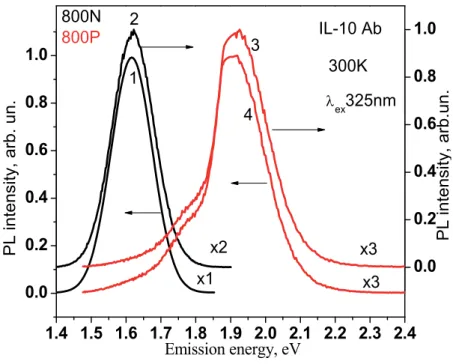
At the same time, the PL intensity of QDs decreases in the case of bioconjugation to anti-IL-10 Ab (Figure 11, curves 3 and 4). At the same time, the PL intensity of the main PL I band decreases and an additional PL band appears in the spectral range of 2.2-3.0 eV.
Discussion of the CdSeTe/ZnS QD bioconjugation
To make the decision about the most likely physical reasons for PL transformation in CdSeTe/ZnS QDs, let us analyze all these factors in detail. i) The emission of HPV or PRV antibodies and PBS can be excited together with the QD emission upon PL excitation by UV light (325 nm). Therefore, the change of the energy band profile in the bi-core CdSeTe/ZnS QDs upon bioconjugation with the charged antibodies allows to explain the features of the PL spectra of the bioconjugated QDs.
Conclusion
Bioconjugation of QDs with charged antibodies stimulates a "blue" energy shift of PL bands associated with exciton emission in CdSe or CdSeTe cores. The change in the energy band profile and the "blue" shift of the QD energy level due to the change in the potential barrier on the QD surface were shown to be the dominant reasons for the transformation of the PL spectrum in the charged antibody-conjugated CdSeTe/ZnS double-core QDs.