Gate Lock Counter Displays the value of the 20-bit counter that gates the latched output of the PLL. Bandwidth Shows the typical and min to max bandwidth value of the PLL in megahertz or kilohertz. Displays the memory initialization file (.mif) generated by the compiler to represent the initial state of the scan chain.
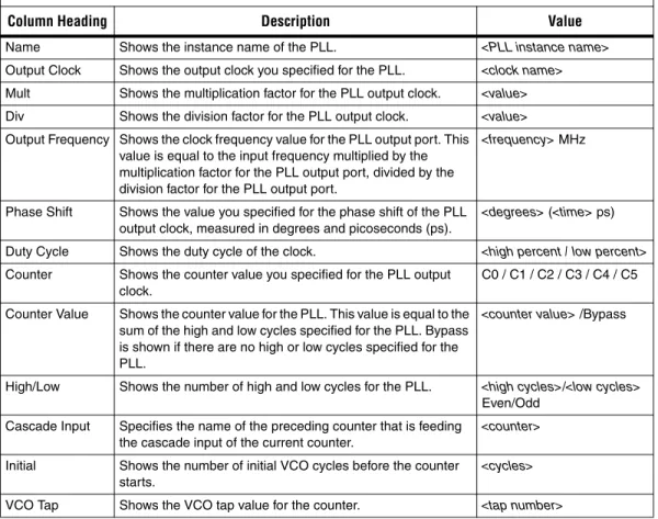
The PLL Usage section reports the values of the specific output clock(s) for the PLLs in the design. Phase Shift Shows the value you specified for the phase shift of the PLL output clock, measured in degrees and picoseconds (ps). This value is equal to the sum of the high and low cycles specified for the PLL.
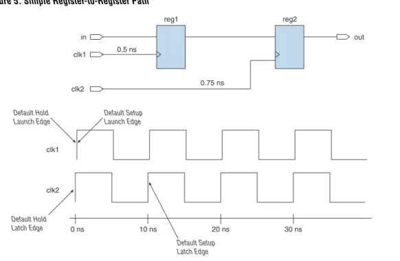
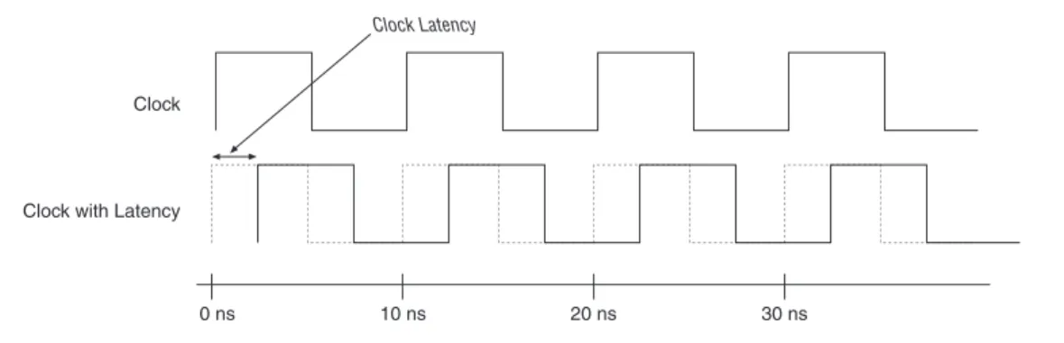
Clock Latency
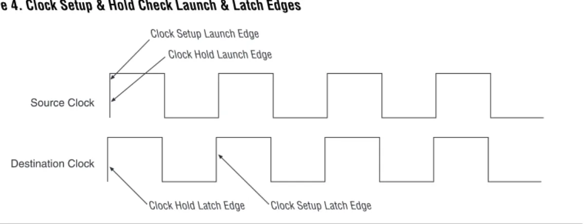
Clock skew = (Shortest clock path to destination register + early clock delay) – (Longest clock path to source register + late clock delay). Clock skew = (longest clock path to destination register + late clock delay) – (shortest clock path to source register + early clock delay). You can specify the clock delay value by using the List Path command on any clock setup or clock hold path.
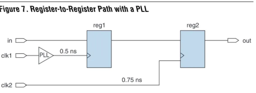
1 Each user-specified phase to one of the PLL's output clocks is modeled as an offset. The clock latency enable option in the Timing Analyzer allows the clock offset to be modeled as clock latency. It does not affect the setup and hold relationships of register-to-register paths.
Enable the clock delay option to prevent setting and hold ratios from changing in designs that contain PLLs.
Clock Switchover
The Timing Analyzer issues a message similar to the one shown in Figure 16 when an individual clock setting overrides the default clock setting on the PLL's input clock pin. When using clock switching, set individual clock settings on the input clock to the PLL and perform a timing analysis for all input clock frequencies and phase shifts. This ensures that the design meets the timing requirements when running at the primary or secondary clock frequency.
This is not necessary if all input clock frequencies and phase shifts are the same.
Clock Uncertainty
Clock Setup Uncertainty Assignment
Clock Hold Uncertainty Assignment
Rerunning the Timing Analyzer increased the required hold relationship from 0.0 ns to 0.5 ns, reducing the backlash time for this design to 0.423 ns (Figure 21).
Application Examples
Aligning the Clock Edges at a Dedicated Clock Input Pin, a Core Register & an External Clock Output Pin
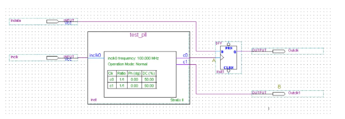
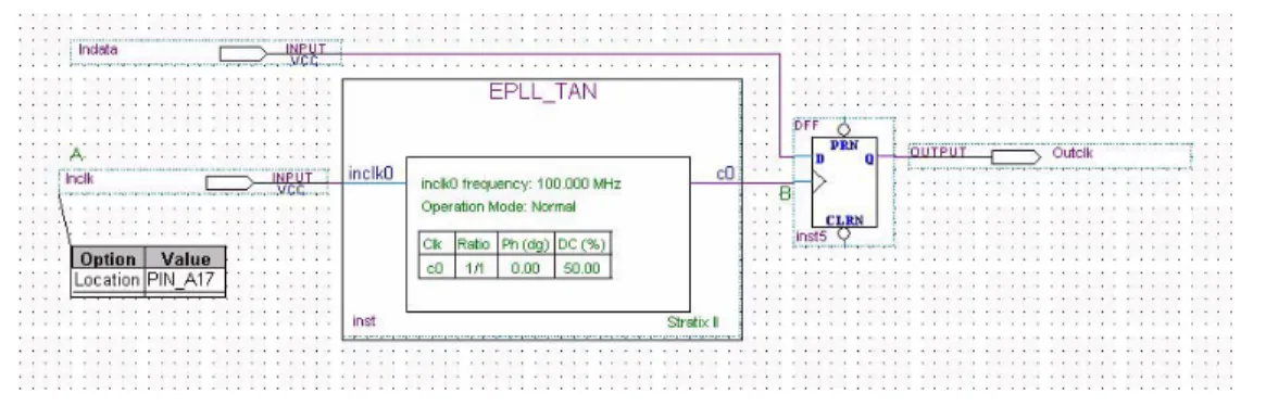
Create the simple PLL register design, shown in Figure 22, and set the PLL to run in normal mode. Normal mode aligns the input clock edge to the PLL (inclk) with the clock edge at the clock gate of the register (A). The path details of the Timing Analysis list show an offset of -2.23 ns between the input clock (inclk) and the C0 clock output of the PLL.
In addition, the Timing Analyzer reports that the shortest clock path from the C0 output of the PLL to point A is 2.203 ns. In effect, this means that the input clock edge is aligned with the clock input at the DFF (A). Expand the tco section of the Timing Report and select List Paths for the PLL output to the output pin (outclk1) (Figure 25).
Expand the Route List in the message window to see a breakdown of delays (Figure 26). The longest clock-to-pin delay is 3.247 ns, and the offset between the clock input and the C1 PLL clock output is -2.23 ns. Since the goal is to align the clock at B with point A and the input clock, you need to introduce a phase shift at the clock output C1 from the PLL.
The granularity of user phase shift depends on the VCO frequency chosen for the design, so the achievable phase shift is very close to, but not equal to, the required 1.017 ns. Select the tco section of the time report and expand the list paths in the message window to see a summary of the delays (Figure 28). The offset reported between the input clock and the C1 clock output port of the PLL is -3.230 ns because a phase offset of -1 ns was added to the standard offset of -2.203 ns.
tCO is now reported as 0.017 ns, so the clock on B leads the input clock by a small margin of 17 ps. If you look at the tsu report for the register, you see that the clock on A is leading the input clock edge by a small margin of 17 ps. Aligning the clock edges on the core register with the non-dedicated clock input pin to the appropriate PLL.
Aligning Clock Edges at a Core Register With a Non-Dedicated Clock Input Pin to the Corresponding PLL
Expand the Global and other fast signals section of the compilation report (Figure 30) to view the exact global resources used to route the clock signals to and from the PLL. Create a test design as shown in Figure 29, and set the PLL to run in normal mode. The timing analysis list detail reports an offset of -0.736 ns between the input clock and the CO clock output of the PLL.
The timing analyzer also reports that the shortest clock path from the C0 output of the PLL to point B is 2.667 ns. This means that the input clock edge is not aligned with the clock at point A (the phase shift of. After recompiling the design, expand the tsu section of the Timing Analysis report and select Path List.
Expand the Paths List in the Messages window to see a breakdown of delays (Figure 34). The shortest clock path from the PLL output gate to point B corresponds to the offset between the input clock and the output clock C1 of the PLL.
PLL Compensation Delay Modeled as Clock Offset Versus Clock Latency
The first scenario shows an analysis with enabling clock latency set to off (clock offset is used). The second scenario shows an analysis with the enable clock latency option set to On (clock latency is used). In this example, the Phase Shift column shows the requested Phase Shift of 36 degrees (1000 ps) based on the output frequency of the PLL.
With the enable clock delay option disabled, each PLL offset delay is modeled as a clock offset. From the clock configuration ratio, the design has a required setup relationship of 1.815 ns and a longer required P2P duration of 0.369 ns. To get more information on the register-to-register path, perform a List-from-report path to generate the report shown in Figure 39.
Consequently, the PLL clock edge at 8.185 ns is taken as the starting edge and the latch edge is taken as the clock edge at 10.0 ns. If the enable clock delay option is set to on, any PLL compensation delay is modeled as a clock delay. From the clock setup report, the design required setup ratio is 9.0 ns and the required maximum P2P time period is 10.169 ns.
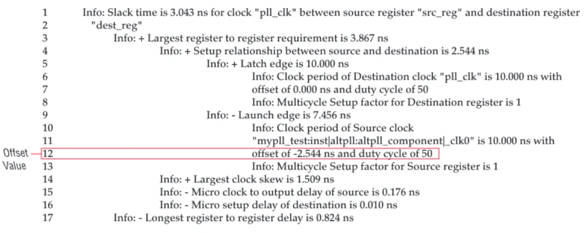
To get more information about the register-to-register path, perform a list path from the report to generate the report shown in Figure 43. The source register, src_reg, is clocked by the output of the PLL with a user-specified phase shift of 36 degrees (1, 0 ns.) Lines 10 and 11 of Figure 43 show this phase shift as an offset of 1.0 ns. 1 Any user-specified or requested phase on the output of the PLLs is modeled as an offset.
With the enable clock delay option enabled, the total PLL offset value can be set in the Clock Skew section of the detailed report. For this design, the clock signal, clock, has an early clock delay assignment of 400 ps and a late clock delay assignment of 600 ps applied to it. The early hour delay value is shown in line 3 of Figure 45, and the late hour delay value is shown in lines 6 and 7.
Clock Multiplexers & Timing Analysis Reports
To determine total PLL compensation based on the value given on lines 6 and 7 of Figure 45, refer to Equation 10. For example, the clock setup report for clk0 shows clock setup analysis where clk0 is the destination clock. In the clock setup report for clk0 and clk1, the register-to-register paths analyzed are from clk1 to clk0 and from clk0 to clk1, respectively.