DEVELOPMENT OF AN EMBEDDED SYSTEM FOR LOW POWER MESSAGE DISPLAY USING SCANNING TECHNIQUE
by
Mohammad Mohidur Rahman Khan
MASTER OF ENGINEERING IN INFORMA nON AND COMMUNICA nON
• TECHNOLOGY
111111111 1111111111111111111111 "'
#10~899#
Institute ofInformation and Communication Technology
BANGLADESH UNIVERSITY OF ENGINEERING AND TECHNOLOGY
August, 2008
The project titled "Development of an Embedded System for Low Power Message Display Using Scanning Technique" submitted by Mohammad Mohidur Rahman Khan, Roll No.
M04053 118, Session April-2005 has been accepted as satisfactory in partial fulfillment of the requirement for the degree of Master of Engineering (ICT) held on 19thAugust, 2008.
BOARD OF EXAMINERS
cW=--_
I. Dr. Md. Liakot Ali Assistant Pro fessor
Institute of Information and Communication Technology BUET, Dhaka-1000.
v 1/~
2. Dr. S. M. Lutful Kabir Professor and Director
Institute ofInformation and Communication Technology BUET, Dhaka-1000.
3. Dr. Md. Abul Kashem Mia Professor and Associate Director
Institute ofInformation and Communication Technology BUET, Dhaka-1000.
Chairman
Member
Member
"
Candidate's Declaration
It is hereby declared that this project or any part of it has not been submitted elsewhere for the award of any degree or diploma.
Mohammad Mohidur Rahman Khan
Dedicated to My Parents
Table of Contents
Title
Board of Examiners Candidate's Declaration Table of Contents List of Fig ures List of Tables Acknowledgement Abstract
Chapter 1: Introduction
1.1 Overview
1.2 Background and present state of the problem 1.3 Objectives with specific aims and possible outcome
Chapter 2: Literature Review
2.1 Display System
2.2 Basic types of Electronic Display
2.2.1 Commonly Used Analog Electronic Display 2.2.2 Commonly Used Digital Electronic Display
2.3 MicrocontrolJer
2.4 Decoder 2.5 Shift Register
2.5.1 Types of shi/i register 2.6 Real Time Clock (RTC)
2.6.1 Purpose 2.6.2 PowerSource 2.6.3 Timing
Chapter 3 Methodology
Page No.
II III
V VII
VIII
IX
X
1
2
3
3 3 3 4 7 8 8 9 11 11 II 12
13
3.1 Introduction
3.2 Analysis of the proposed system 3.3 Block Diagram of the system 3.4 Devices used for the proposed system
3.4.1 Atmel ATMEGA88 -8bit Microconlroller
3.4.2 BCD 107-segmenl latch/decoder/driver (CD4511 BE) 3.4.38 bil Serial-Input Parallel- Outpul Shift Register (74HCI64) 3.4.4 Real Time Clock (DS1307)
3.5 Softwares Used For the Proposed System 3.5.1 WinAVR
3.5.2 A VR Studio 5.0 3.5.3 Easy-PC 4.0 3.5.4 Circuit Maker 4.0
Chapter 4: Results and Discussions
4.1 Introduction 4.2 Schematic Design
4.3 Printed Circuit Board (PCB) Design 4.4 The Artview of the Proposed System 4.5 Result
Chapter 5: Conclusion
5.1 Conclusion
5.2 Suggestions for Future Works
References Appendix A
13
13 13 15 15 16 18 19 20 20
21 21 21
22
22 22 24 24 24
24
24 24
24
24
List of Figures
Title
Figure 2.1: Cathode Ray Tube (CRT) Display
Figure 2.2: Different Types of Light Emitting Diode (LED) Figure 2.3: Seven Segment Display
Figure 2.4: Segments of a 7-Segment Display Figure 2.5: Microcontroller
Figure 2.6: 4-Bit SIPO Shift Register Figure 2.7: 4-Bit PI SO Shift Register
Figure 3.1: Block Diagram of the Proposed System Figure 3.2: Pinning Diagram Atmega88
Figure 3.3: Pinning Diagram of 7-Segment Decoder Figure 3.4: Logic Diagram of74HCI64
Figure 3.5: Pin Assignment of74HCI64 Figure 3.6: Pin Assignment Of OS 1307 Figure 3.7: DSI307 Address Map
Figure 3.8: OS 1307 Time Keeper Register
Figure 4.1: Schematic Diagram of the Proposed System Figure 4.2 PCB Diagram of the Proposed System Figure 4.3 The Artview of the Proposed System
Page No.
4 4 6 6 7 10
II 14
16
17
18 18
19
19
20 24 26
27
List of Tables
Title
Table 3.1: Fuction Table of7-Segment Decoder Table 3.2: Fuction Table of74hcl64
Table 3.3: DS1307 Square Wave Output Frequency Table 4.1: Current Consumption of the System
Page No 17 19 20 28
Acknowledgement
First of all I would like to thank the almighty Allah for giving me the opportunity to conduct this project. I would like to express my sincere thanks to my project supervisor, Dr. Md. Liakot Ali, for giving me the opportunity to conduct this project. I am grateful to pursue my project under his supervision. Without his ever helping personalities, this project would not have got the success.
I would like to convey my thanks to Professor Dr. S. M. Lutful Kabir, Director, lICT, BUET. His motivation and inspiration gave me the courage to do this work.
I gratefully acknowledge the restless support and advice of my fellow classmate and friend Md. Faruq Ahmed Jewel during the design and implementation phase of this project. I want to convey my thanks to one of my very good friends Nowshad Ibne Alam (Arnob) for giving his valuable time while I was buying the apparatus for my project. My thanks also go to another very good friend Md. Sabbir Hasan for his support during the documentation phase of the project. My special thanks to all the teachers, students and staffs oflICT, BUET.
I would like to thanks all my friends for their continuous support and inspiration
throughout the whole period of this undertaking.
Abstract
Electronic display is now the most conventional means of presenting information all over the world. Due to its attractive brightness and simple operability, it is one of the most popular medium of presenting different types of information to the mass people. The display elements in an embedded system consume the major portion of the total power required to run the whole system. When large amount of display elements are used power dissipation issue becomes acute. In many cases special cooling arrangements like heat sink, cool air circulation, fan etc. are used to keep the system workable. The demand of low power consumption for embedded systems motivates to explore new approaches for managing power. This project proposes an alternative approach to develop a low power consuming embedded system for message display by introducing a new scanning technique. In the proposed system a controller scans all the display units continuously to ensure that only one unit is on at any given time. In this way power consumption will be much lower than that of existing static display system. Here a 'Muslim Calendar' containing date, time and prayer times for five salah has been developed as a test case.
Seven segment displays are used as display units.
1.1 Overview
Chapter 1 Introduction
Electronic display-we see it everywhere, in computers, watches, DVD players and many other electronic devices to display numeric and some alphabetic characters. It is also used for showing messages in digital calendars, billboards, shopping malls, airports, stadiums and many other places. It is a commonly used and efficient way of displaying information. The use of electronic displays for presentation of graphs, symbols, alphanumerics, and still or video pictures has doubled every several years, in parallel with the rapid expansion of microelectronics. Electronic displays have largely replaced traditional mechanical devices, counters, galvanometers, and to a degree, hardcopy (paper) means for presenting information.
This change is due to the increased use of computers, microprocessors, inexpensive large- scale integration (LSI) electronics, and digital mass memories.
Although electronic display is widely used, power consumption is still an important issue. In an electronic circuit, the major part of the total power is consumed by the display elements. If a large amount of display units are used in a system then the power requirement to run the system will also increase proportionately. In that case extra cooling arrangements may be required to keep the system workable. So the demands of low power consumption for embedded systems are motivating new approaches to manage power dissipations issues.
1.2 Background and Present State of the Problem
A lot of research works have been done for displaying numeric digits of languages other than English where the researchers used Seven Segment Display or some modification on it [1-3].
Display is one of the major power consumers in modern computer system [4]. Power consumption is even more critical when multiple display units are used together for displaying message. In some cases, it needs extra cooling arrangements for heat dissipation. Researchers
'.
have proposed plasma screen or organic light-emitting devices (OLEO) to reduce power consumption for display element [5, 6]. So reducing the power consumption for display element is an important research area.
1.3 Objectives with Specific Aims and Possible Outcome:
The major objectives of the project are as follows.
i) To study different types of display devices, ii) To develop small prototypes on the bread-board, iii) To design a Printed Circuit Board (PCB) and iv) To implement the proposed system on the PCB.
Here as a test case a calendar will be developed where the following information will be displayed using seven segment display.
a) Date, b) Time and
c) Prayer times of five salah for any given date.
1.4 Organization of the Project
Chapter I of this report starts with impact of power consumption in the digital circuits by display units followed by a brief background of power dissipation issues of electronic display, objectives and organization of this report.
In Chapter 2 of this report, issues from all aspects in developing the proposed system have been reviewed.
Detail methodology of the proposed system has been discussed elaborately in chapter 3.
In chapter 4 step by step design and development and obtained result of the proposed system have been discussed.
In the final chapter (Chapter 5) conclusion and recommendation for future works has been stated.
The project report ends with an appendix that contains the program code of the system.
Chapter 2 Literature Review
2.1 Display System
A display device is a device for presentation of information for visual reception, acquired, stored, or transmitted in various forms. When the input information is supplied as an electrical signal, the display is called "electronic display". An electronic component used to convert electrical signals into visual imagery in real time suitable for direct interpretation by a human operator. It serves as the visual interface between human and machine. The visual imagery is processed, composed, and optimized for easy interpretation and minimum reading error.
2.2 Basic types of Electronic Display
There are two basic types of displays. They are:
• Analog Electronic Display
• Digital Electronic Display
The following subsections briefly describe different types of displays systems that are commonly used.
2.2.1 Commonly Used Analog Electronic Display
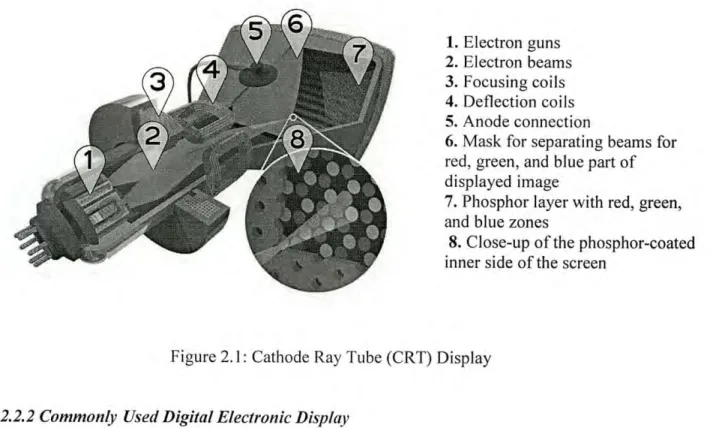
The cathode ray tube (CRT) display is the most commonly used analog electronic display.
The cathode ray tube (CRT) is a vacuum tube containing an electron gun (a source of electrons) and a fluorescent screen, with internal or external means to accelerate and deflect the electron beam, used to form images in the form of light emitted from the fluorescent screen. The image may represent electrical waveforms (oscilloscope), pictures (television, computer monitor), radar targets and others.
The single electron beam can be processed in such a way as to display moving pictures in natural colors.
1. Electron guns 2. Electron beams 3. Focusing coils 4. Deflection coils 5. Anode connection
6. Mask for separating beams for red, green, and blue part of displayed image
7. Phosphor layer with red, green, and blue zones
8. Close-up of the phosphor-coated inner side of the screen
Figure 2. I : Cathode Ray Tube (CRT) Display
2.2.2 Commollly Used Digital Electrollic Display
There are many examples of digital electronic displays. Among them light emitting diode (LED), liquid crystal display (LCD) and seven segment display are most common.
a) Light Emitting Diode (LED)
A light-emitting diode is a semiconductor diode that emits incoherent narrow-spectrum light when electrically biased in the forward direction of the p-n junction, as in the common LED circuit. This effect is a form of electroluminescence.
Figure 2.2: Different types of Light Emitting Diode (LED)
An LED is usually a small area light source, often with optics added to the chip to shape its radiation pattern. LEOs are often used as small indicator lights on electronic devices and increasingly in higher power applications such as flashlights and area lighting. The color of
the emitted light depends on the composition and condition of the semiconducting material used, and can be infrared, visible, or ultraviolet. LEOs can also be used as a regular household light source. Besides lighting, interesting applications include sterilization of water and disinfection of devices.
b) Liquid Crystal Display (LCD)
A liquid crystal display (LCD) is a thin, flat display device made up of any number of color or monochrome pixels arrayed in front of a light source or reflector. A low-power flat-panel display used in many laptop computers, calculators and digital watches, made up of a liquid crystal that is sandwiched between layers of glass or plastic and becomes opaque when electric current passes through it. The contrast between the opaque and transparent areas forms visible characters.
LCD is a display technology that uses rod-shaped molecules (liquid crystals) that flow like liquid and bend light. When not energized, the crystals direct light through two polarizing filters, allowing a natural background color to show. When energized, they redirect the light to be absorbed in one of the polarizers, causing the dark appearance of crossed polarizers to show. The more the molecules are twisted, the better the contrast and viewing angle.
Because it takes less power to move molecules than to energize a light-emitting device, LCOs replaced the light-emitting diodes (LEOs) in digital watches in the 1970s. LCOs were then widely used for a myriad of monochrome displays and still are. In the 1990s, color LCD screens caused sales of laptop computers to explode, and in 2003, more LCD monitors were sold for desktop computers than CRTs.
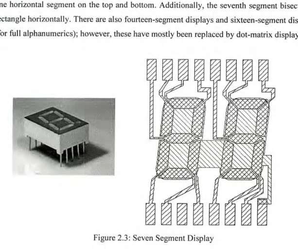
c) Seven Segment Display
A common display found on digital watches and readouts that looks like a series of 8s. Each digit is formed by selective illumination of up to seven separately addressable bars.
A seven segment display, as its name indicates, is composed of seven elements. Individually on or off, they can be combined to produce simplified representations of the Hindu-Arabic numerals. Often the seven segments are arranged in an oblique, or italic, arrangement, which aids readability.
The seven segments are arranged as a rectangle of two vertical segments on each side with one horizontal segment on the top and bottom. Additionally, the seventh segment bisects the rectangle horizontally. There are also fourteen-segment displays and sixteen-segment displays (for full alphanumerics); however, these have mostly been replaced by dot-matrix displays.
Figure 2.3: Seven Segment Display
The segments of a 7-segment display are referred to by the letters A to G, as shown bellow, where the optional DP decimal point (an "eighth segment") is used for the display of non- integer numbers.
Figure 2.4: Segments of a 7-segment display
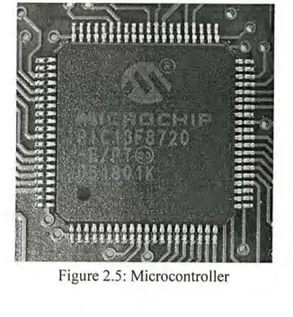
2.3 Microcontroller
A microcontroller (also MCU or !!C) is a computer-on-a-chip, containing a processor, memory, and input/output functions. It is a microprocessor emphasizing high integration, in contrast to a general-purpose microprocessor (the kind used in a PC). Inaddition to the usual arithmetic and logic elements of a general purpose microprocessor, the microcontroller integrates additional elements such as read-write memory for data storage, read-only memory for program storage, EEPROM for permanent data storage, peripheral devices, and input/output interfaces. At clock speeds of as little as a few MHz or even lower, microcontrollers often operate at very low speed compared to modern day microprocessors, but this is adequate for typical applications. They consume relatively little power (milliwatts), and will generally have the ability to sleep while waiting for an interesting peripheral event such as a button press to wake them up again to do something. Power consumption while sleeping may be just nanowatts, making them ideal for low power and long lasting battery appl ications.
Microcontrollers are frequently used in automatically controlled products and devices, such as automobile engine control systems, remote controls, office machines, appliances, power tools, and toys. By reducing the size, cost, and power consumption compared to a design using a separate microprocessor, memory, and input/output devices, microcontrollers make it economical to electronically control many more processes.
Figure 2.5: Microcontroller
A microcontroller is a single integrated circuit, commonly with the following features:
• central processing unit - ranging from small and simple 4-bit processors to complex 32- or 64-bit processors
• discrete input and output bits, allowing control or detection of the logic state of an individual package pin
• serial input/output such as serial ports (VARTs)
• other serial communications interfaces like FC, Serial Peripheral Interface and Controller Area Network for system interconnect
• peripherals such as timers and watchdog
• volatile memory (RAM) for data storage
• ROM, EPROM, [EEPROM] or Flash memory for program and operating parameter storage
• clock generator - often an oscillator for a quartz timing crystal, resonator or RC circuit
• many include analog-to-digital converters
2.4 Decoder
Decoder is a multiple-input, multiple-output logic circuit that converts coded inputs into coded outputs, where the input and output codes are different. e.g. n-to-2n, BCD decoders.
Enable inputs must be on for the decoder to function, otherwise its outputs assume a single
"disabled" output code word. Decoding is necessary in applications such as data multiplexing, 7 segment display and memory address decoding.
The simplest decoder circuit would be an AND gate because the output of an AND gate is
"High" (I) only when all its inputs are "High".
2.5 Shift Register
In digital circuits a shift register is a group of flip flops set up in a linear fashion which have their inputs and outputs connected together in such a way that the data is shifted down the line when the circuit is activated.
2.5.1 Types of Shift Register
Shift registers can have a combination of serial and parallel inputs and outputs, including serial-in, parallel-out (SIPO) and parallel-in, serial-out (PISO) types. There are also types that have both serial and parallel input and types with serial and parallel output. There are also bi- directional shift registers which allow you to vary the direction of the shift register. The serial input and outputs of a register can also be connected together to create a circular shift register.
One could also create multi-dimensional shift registers, which can perform more complex computation.
i) Serial-In, Serial-Out aj Destructive readout:
These are the simplest kind of shift register. The data string is presented at 'Data In', and is shifted right one stage each time 'Data Advance' is brought high. At each advance, the bit on the far left (i.e. 'Data In') is shifted into the first flip-flop's output. The bit on the far right (Le.
'Data Out') is shifted out and lost.
The data are stored after each flip-flop on the 'Q' output, so there are four storage 'slots' available in this arrangement, hence it is a 4-Bit Register. To give an idea of the shifting pattern, imagine that the register holds 0000 (so all storage slots are empty). As 'Data In' presents I, I,0, I,0,0,0,0 (in that order, with a pulse at 'Data Advance' each time. This is called clocking or strobing) to the register, this is the result. The left hand column corresponds to the left-most flip-flop's output pin, and so on.
So the serial output of the entire register is J J
°
J 0000. As one can see if we were to continue to input data, we would get exactly what was put in, but offset by four 'Data Advance' cycles.This arrangement is the hardware equivalent of a queue. Also, at any time, the whole register can be set to zero by bringing the reset (R) pins high.
bj Non-destructive Readout
Non-destructive readout can be achieved using the configuration shown below. Another input line is added - the Read/Write Control. When this is high (i.e. write) then the shift register behaves as normal, advancing the input data one place for every clock cycle, and data can be
lost from the end of the register. However, when the R/W control is set low (i.e. read), any data shifted out of the register at the right becomes the next input at the left, and is kept in the system. Therefore, as long as the RlW control is set low, no data can be lost from the system.
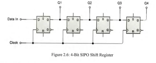
ii.Serial-In, Parallel-Out
This configuration allows conversion from serial to parallel format. Data are input serially, as described in the SISO section above. Once the data has been input, it may be either read off at each output simultaneously, or it can be shifted out and replaced.
Data In
o
S Qo
I o
S QR Q
I o
S QR Q
03
I o
S QR Q 04
J
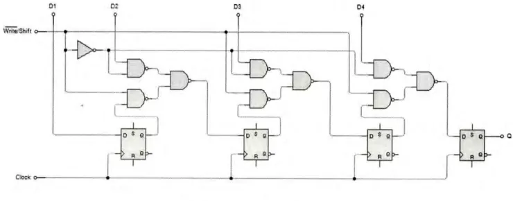
iii.Parallel-In, Serial-Out
Figure 2.6: 4-Bit SIPO Shift Register
This configuration has the data input on lines D I through D4 in parallel format. To write the data to the register, the Write/Shift control line must be held LOW. To shift the data, the W/S control line is brought HIGH and the registers are clocked. The arrangement now acts as a SISO shift register, with D I as the Data Input. However, as long as the number of clock cycles is not more than the length of the data-string, the Data Output, Q, will be the parallel data read off in order.
01 0' 0' o.
--l>-r
Cio<ko~---f 1.-- R_' __
f
R 'f
Figure 2.7: 4-Bit PISO Shift Register
o $ Q C
R •
2.6 Real Time Clock (RTC)
A real-time clock (RTC) is a computer clock (most often in the form of an integrated circuit) that keeps track of the current time. Although the term often refers to the devices in personal computers, servers and embedded systems, RTCs are present in almost any electronic device which needs to keep accurate time.
2.6.1 Purpose
Although keeping time can be done without an RTC, using one has benefits:
• Low power consumption (important when running from alternate power)
• Frees the main system for time-critical tasks
• Sometimes more accurate than other methods (although personal computer RTC's are often inaccurate)
2.6.2 Power Source
RTCs often have an alternate source of power, so they can continue to keep time while the primary source of power is off or unavailable. This alternate source of power is normally a lithium battery in older systems, but some newer systems use a supercapacitor, because they are rechargeable and can be soldered. The alternate power source can also supply power to battery backed RAM.
2.6.3 Timing
Most RTCs use a crystal oscillator, but some use the power line frequency. In many cases the oscillator's frequency is 32.768 kHz.This is the same frequency used in quartz clocks and watches, and for the same reasons, namely that the frequency is exactly 215 cycles per second, which is a convenient rate to use with simple binary counter circuits.
Chapter 3 Methodology
3.1 Introduction
In electronic circuits the issue of managing heat and power dissipation has become increasingly significant. The display units are the major power consuming units of an electronic circuit. Power consumption increases when the size or the number of display units increases. Sometimes it requires extra cooling arrangements for large display units. Besides one has to ensure that the Power Supply unit he/she uses for the circuit is good enough to supply enough current to illuminate the display units.
3.2 Analysis of the Proposed System
This project concentrates on the power dissipation issues for display devices. A scanning technique has been introduced in the proposed to minimize the power consumption for display elements. The objective is to connect all the display elements in parallel with each other and turning only one unit on at a time for a very short period and move to the next unit. If each unit can be illuminated periodically in a very short span of time the human eye will see the entire message as if all the units are turned on whereas only one unit is on at any given time.
Here seven segment displays are used as display units and as a test case a Muslim Calendar is developed with 30 units of seven segment display. As the algorithm for illuminating display units follow the scanning technique only one unit of seven segment display is turned on at any given time. So theoretically the total power consumption for illuminating display units is reduced by 30 times. Hence 30 units of seven segment displays can be illuminated by only the power required by one unit.
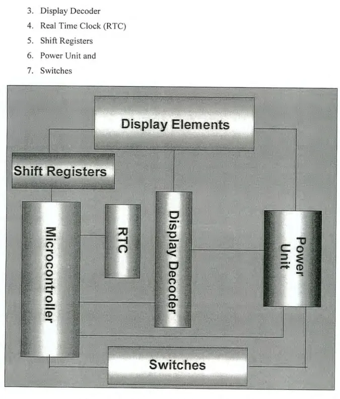
3.3 Block Diagram of the system
The basic units of the proposed system can be divided into the following 7 Parts.
I. Microcontroller 2. Display elements
3. Display Decoder
4. Real Time Clock (RTC) 5. Shift Registers
6. Power Unit and 7. Switches
Display Elements
Switches
Figure 3.1: Block diagram of the proposed system
Here the microcontroller controls the input of the shift registers. The output of the shift registers are connected to the common cathodes of 30 seven segment displays. The microcontroller initializes all the output pins of the shift register at level 1 (sends logic 1 thirty times in the input of the shift registers), making all the seven segment displays to be turned
off. At this point the microcontroller sends logic 0 once and logic I 29 times so that each display receives the signal 0 sequentially while other displays receive signal I. In this process, only one display is turned at a time and shifted sequentially.
The output pins of the display decoder are connected in parallel to all seven segment displays.
The Microcontroller sends appropriate input for the decoder when corresponding seven segment display has logic 0 at its common cathode.
A real time clock is used to keep the date and time. The microcontroller reads time from the RTC each minute and changes the display clock and date accordingly. The prayer time table is loaded in the program memory of the microcontroller as an array of structure (see Appendix A). The prayer times change with the change of day and month field of the date. There is a battery connected to the RTC so that it can keep the time and date when the main power is not available.
Three switches are used to set time and date. One switch is used to select which field of the time and date is to be changed. Other two switches are used to count up and count down the selected field. All these operation is controlled by the microcontroller.
3.4 Devices Used for the Proposed System
Some chips/devices have been used for the proposed system. Brief description on those devices is given bellow.
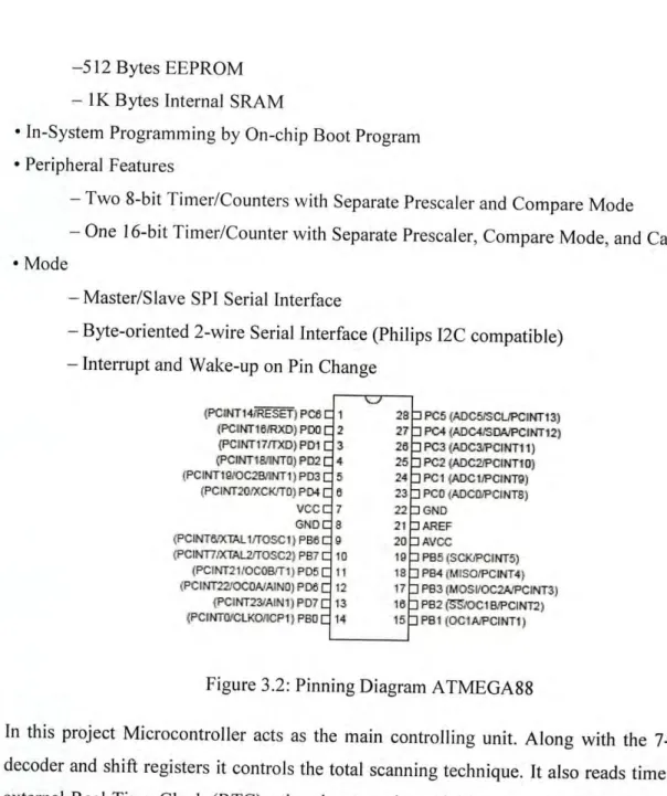
3.4.1 Atmel ATMEGA88 - 8bit Microcontroller
Here this specific microcontroller is used for its following special features .
• Advanced RISC Architecture
- 131 Powerful Instructions - Most Single Clock Cycle Execution - 32 x 8 General Purpose Working Registers
- Fully Static Operation
- Up to 20 MIPS Throughput at 20 MHz
• High Endurance Non-volatile Memory segments
- 8K Bytes of In-System Self-programmable Flash program memory
-512 Bytes EEPROM - IK Bytes Internal SRAM
• In-System Programming by On-chip Boot Program
• Peripheral Features
- Two 8-bit Timer/Counters with Separate Prescaler and Compare Mode
- One 16-bit Timer/Counter with Separate Prescaler, Compare Mode, and Capture
• Mode
- Master/Slave SPI Serial Interface
- Byte-oriented 2-wire Serial Interface (Philips 12C compatible) - Interrupt and Wake-up on Pin Change
(PClNT14lRESET) PC6 (PCINT16/RXD) PDQ (pcINT17/TXD) po, (PCINT1811NTD) PD2 (PCINT1P/OC2S,.riNT1) P03
(PC1NT20lXCKfTO) P04
vcc DND (PCINT6IXTAllfTOSC t)PB/3 (PCINT7JXTAL2fTOSC2) PB7
(PCtNT21,'OCOBJT1) P05 (PCINT22'OCONAINO) Poe
(PCINT231AIN1) PD7 (PCINTOlCLKOIICP1) PBO
pe5 (AOC5lSCLJPC1NT13) POt. (AOC4lSOAJPCINT12) PC3 (ADC~?CINTll) PC2 (AOC2iPCINTlD) PCl (ADC1IPCINTD) PeO (ADCQ;PCINT8)
GND AREF Avec
PBS (SClVPCINT5) P84 (M1SO,'PCINT4) PB3 (MOS"OC2A ?CINT3) P82~'OC1B,IPC1NT2) PBl (OC1AiPCINT1)
Figure 3.2: Pinning Diagram A TMEGA88
In this project Microcontroller acts as the main controlling unit. Along with the 7-segment decoder and shift registers itcontrols the total scanning technique. It also reads time from an external Real Time Clock (RTC) using the two wire serial interface. Pin Change interrupt of the microcontroller is used to blink the LEOs used for showing time.
The Microcontroller has 8KB Flash program memory where the prayer times for one year is saved as an array. This array is used to display the prayer times for any particular day of a month.
3.4.2 BCD to 7-segment latch/decoder/driver (CD4511BE)
The CD4511BE is a BCD to 7-segment latch/decoder/driver with four address inputs (DA to DD), an active LOW latch enable input (EL), an active LOW ripple blanking input (BI), an
active LOW lamp test input (LT), and seven active HIGH n-p-n bipolar transistor segment outputs (Oa to Og). When EL is LOW, the state of the segment outputs (Oa to Og) is determined by the data on DA to DD. When EL goes HIGH, the last data present on DA to DD are stored in the latches and the segment outputs remain stable. When LT is LOW, all the segment outputs are HIGH independent of all other input conditions. With LT HIGH, a LOW on BI forces all segment outputs LOW. The inputs LT and BI do not affect the latch circuit.
HEF4511 B
7273716.1
Figure 3.3: Pinning Diagram of7-Segment Decoder
Table 3.1: Fuction Table of7-Segment Decoder
INPUTS OUTPUTS
EL BI LT Do Dc DB DA 0. 0" 0.
°d
0. 0, 0. DISPLAYX X L X X X X H H H H H H H 8
X L H X X X X L L L L L L L blank
L H H L L L L H H H H H H L 0
L H H L L L H L H H L L L L 1
L H H L L H L H H L H H L H 2
L H H L L H H H H H H L L H 3
L H H L H L L L H H L L H H 4
L H H L H L H H L H H L H H 5
L H H L H H L L L H H H H H 6
L H H L H H H H H H L L L L 7
L H H H L L L H H H H H H H 8
L H H H L L H H H H L L H H 9
L H H H L H L L L L L L L L blank
L H H H L H H L L L L L L L blank
L H H H H L L L L L L L L L blank
L H H H H L H L L L L L L L blank
L H H H H H L L L L L L L L blank
L H H H H H H L L L L L L L blank
H H H X X X X
.
3.4.3 8bit Serial-Input Parallel- Output Shift Register (74HCI64)
The MC54174HC 164 is an 8-bit, serial-input to parallel-output shift register. Two serial data inputs, A 1 and A2, are provided so that one input may be used as a data enable. In this project A I and A2 pins are made short as no data enable is required. Data is entered on each rising edge of the clock. The active-low asynchronous Reset overrides the Clock and Serial Data inputs.
SERIALIAI 1
DATA 2
INPUTS IV.
CLOCK B
RESET 9
DATA
PIN 14=Vee
PIN 1 ~GND
PARALLEl DATA OUTPUTS
Figure 3.4: Logic Diagram of74HC164
Al 1 • 14 VCC
A2
2 13QH
QA 3
12QG
QB
4 11QF
QC 5
10QE
QD 6 9 RESET
GND 7 8 CLOCK
Figure 3.5: Pin Assignment of74HCI64
Table 3.2: Fuction Table of74HCI64
Inputs Outputs
Reset Clock
A1 A2 OA Os ... OH
L X X X L L
...
LH \.... X X No Change
H f H D D QAn ... QGn
H f D H D QAn ... QGn
D = data input
QAn - QGn
=
data shifted from the preceding stage on a rising edge at the clock input.3.4.4 Real Time Clock (DSI307)
The OS 1307 Serial Real Time Clock is a low power, full BCD Clock/Calendar plus 56 bytes of nonvolatile SRAM. Address and data are transferred serially via a 2-wire bi-directional bus. The Clock/Calendar provides seconds, minutes, hours, day, date, month and year information. The end of the month date is automatically adjusted for months with less than 31 days, including corrections for Leap Year. The clock operates in either the 24 hour or 12 hour format with AM/PM indicator. The OS 1307 has a built-in power sense circuit which detects power failures and automatically switches to the battery supply.
x, [lV,
v",Xl 2 7 saW/OUT
v••, J l! sel
GND ~ 5 SOA
Figure 3.6: Pin Assignment of OS 1307
OOH
07H 08H
3FH
SECONDS
MINUTES HOURS
DAY DATE
J.1ONTH
YEAR
CONTROL
RAM
5th 8
Figure 3.7: OS 1307 Address Map
I ." I
CH "~ "'ex><>s
,
10 Wl"",Tn WltAlJES, IX "
~" ...
HOUAS""
• , • , , I
D"• ,
"om"''''
• , • 1..I.:n. ..,,~
w'"'''' '''''
OUT
I ' • ""'" .1.[ ••,[ .•••
01-12
Figure 3.8: OS 1307 Time Keeper Register Table 3.3: OS 1307 Square Wave Output Frequency
RSI RSO SOW OUTPUT FREOUENCY
0 0 1Hz
0 1 4.096kHz
1 0 8.192kHz
1 1 32.76SkHz
3.5 Softwares Used for the Proposed System
The following softwares were used to develop the proposed system.
3.5.1 WinA VR
The WinAVR Library package provides a subset of the standard C library for Atmel A VR 8- bit RISC microcontrollers. In addition, the library provides the basic startup code needed by most applications.
In general, it has been WinA VR's goal to stick as best as possible to establish standards while implementing this library. Commonly, this refers to the C library as described by the ANSI X3.159-1989 and ISO/IEC 9899:1990 ("ANSI-C") standard, as well as parts of their successor ISO/IEC 9899: 1999 ("C99"). Some additions have been inspired by other standards like IEEE Std 1003.1-1988 ("POSIX.I"), while other extensions are purely AVR-specific (like the entire program-space string interface).
Unless otherwise noted, functions of this library are not guaranteed to be reentrant. In particular, any functions that store local state are known to be non-reentrant, as well as functions that manipulate 10 registers like the EEPROM access routines. If these functions are used within both standard and interrupt contexts undefined behavior will result.
3.5.2 AVR Studio 5.0
A VR Studio is an Integrated Development Environment (IDE) for writing and debugging AVR applications in Windows 9x/MEINTI2000/XP/VIST A environments. A VR Studio provides a project management tool, source file editor, simulator, assembler and front-end for C/C++, programming, emulation and on-chip debugging.
AVR Studio supports the complete range of ATMEL AVR tools and each release will always contain the latest updates for both the tools and support of new A VR devices.
A VR Studio 4 has a modular architecture which allows even more interaction with 3rd party software vendors. GUI plug-ins and other modules can be written and hooked to the system.
3.5.3 Easy-PC 4.0
This software is a PCB designing tool for Windows. Easy-PC really is the latest generation of PCB CAD with no other product currently as advanced or in-line with the Microsoft operating systems - Windows 95/98 and NT. And because Easy-PC has been written using the latest software techniques, object oriented code (C++) and under Windows NT as a true Windows 32 bit application, it can be easily enhanced to accommodate new demands in technology and customer feedback.
3.5.4 Circuit Maker 4.0
CircuitMaker is a powerful, easy-to-use schematic capture and simulation tool in its class.
CircuitMaker provides the features of "high-end" design software at a fraction of the cost.
Using CircuitMaker's advanced schematic capabilities; one can design electronic circuits and output netlists for TraxMaker and other PCB design tools and autorouters. One can also perform fast, accurate simulations of digital, analog and mixed analog/digital circuits using CircuitMaker's Berkeley SPICE3f5/XSpice-based simulator.
Chapter 4 Results and Discussions
4.1 Introduction
This chapter describes the schematic design and printed circuit board (PCB) design of the proposed system. The Artview of the proposed system is also given here. At the end of this chapter the implementation results of the proposed system are presented.
4.2 Schematic Design
Figure 4.1 shows the schematic design of the proposed project. The main part of the project is the Atmel ATMEGA88 microcontroller. All other components are connected to it and controlled by it. The four input pins (00-03) of the seven segment decoder (C045 I 1BE) are connected to the first four pins of port B (PBO-PB3) of the microcontroller. These pins are used to provide the appropriate data to be displayed by a particular seven segment display.
The seven output pins (a-g) of the display decoder are connected to all seven segment displays' input pins (a-g) in parallel along with seven 100
n
registers.Four shift registers (74HCI64) are used in this project. The input pins (Osa & Osb) of the first shift register are made short and is connected to the second pin of the Port C (PC I) of the microcontroller. The clock pin (CP) of the shift register is connected to the first pin of the Port C (PCO) of the microcontroller. Each pair of input pins of the rest three shift registers are made short just like the fist one and is connected to the last output pin (Q7) of the immediate previous one. All the output pins of the shift registers are connected to the common cathode of the seven segment displays sequentially.
The SOA and SCL pins of the Real Time Clock is connected to the fifth (PC4) and sixth (PC5) pin of the Port C of the microcontroller. Two pull up registers are also connected to these pins. The SQW pin of the RTC is connected to the fourth pin (PC3) of the Port C of the
microcontroller. A 3.2786 MHz crystal is connected to Xl and X2 pins of the RTC and a 3 volt battery is also connected to its Vb" and GND pin.
Three input switches are connected to the third fourth and fifth pin of Port D (PD2-PD4) of the microcontroller. These three pins are made ground with three IOkO registers.
74LS164,
'Du 0
Dsb Q
Q Q Q Q Q Q 74LS164
:Dsa 071
Dsb 06
Q' Q'g~1
"
Q
5V~
O.33k DlSP96 DISPl
~rGnd
'"'
DlSPl
'"'
5V 'V
abed ••
'"'
sbedet<l.t[abed, DlSP!.Q...plSP2
'"'
DlSPl
Figure 4.1: Schematic diagram of the proposed system
4.3 Printed Circuit Board (PCB) Design
To design the PCB, a software named Easy PC has been used. Definitions of some components were not found in the software. In those cases the components were made manually by putting Pads according to their Pin configuration.
Fig. 4.2 shows the PCB diagram of the proposed project. It is a single layer PCB. The red lines indicate the top copper routing of the Circuit Board. Some jumps have to be made to make the circuit fully functional. In those cases some extra wire connection has been made.
E
"
~
'"
~
'"
o0-
e
0-
"
-5'-o
4.4 The Artview of the Proposed System
After putting all the components on the circuit board and programming the microcontroller the total system looks like as follows.
Figure 4.3 The Artview of the Proposed System
Here the first block of four (top left corner) seven segment displays shows time. First two units of this block represent hour while second two represent minute. The second block of six (top right corner) seven segment displays represents date where the first, second and third two units of the block represent day, month and year respectively. The remaining five blocks of four seven segment displays represent the prayer times of five salah; Fazr, Zurh, Asr, Maghrib and Esha as labeled in the figure 4.3. Here each first two units of each block represent hour and the remaining two units of each block represent minute.
There are three buttons: Mode, Up and Down. The Mode button selects which unit of time or date is to be changed. Then the buttons Up and Down are used to count up or down respectively to set the selected unit of time or date.
4.5 Result
Scanning technique is a power aware solution for message display. Here we have used 30 seven segment displays. But as scanning technique is applied, at any given time only one seven segment display is on. So, theoritically the system should consume 1/30times less power than it would take to make all the seven segment displays on at a time.
But following table shows the practical senario.
Table 4.1: Current and Power Consumption by the Display Elements
Current and Power Consumpiin for 30 Units of Seven Segment Displays
With Scanning Technique Without Scanning Technique
Curren Consumption 18mA 75mA
Power Comsumption 0.09 watt 0.375 watt
So, in practical the power consumption is not as less as 30 times of the total power needed.
But still it minimizes the power consumption to a considerable amount that is 76% less power is required to run the display units of the system when the scanning technique is applied.
Another important point is for the scanning technique only one Display Decoder is used. If this technique is not applied then 30 Display Decoders should be used for 30 seven segment display. Furthermore a microcontroller has limited number of pins. So, a commonly used microcontroller may not be able to connect all the display decoders at a time due to its fixed number of pins.
So, the solution enables a circuit to be operated in less power, less area hence less cost.
Chapter 5 Conclusion
5.1 Conclusion
Power management has a considerable importance in electronic circuits. In electronic displays, power consumption increases with the size and number of the display units. This project uses scanning technique to reduce power consumption. The embedded system developed as a test case demonstrates a power aware solution using scanning technique. The seven segment displays used as display units consume less power when scanning technique is used. Since the algorithm allows only one display unit to be illuminated at any given time rather than all the units receiving power, it consumes significant less power. The scanning technique in the embedded circuit requires only one Display Decoder for all the display units.
Scanning technique can be used in numerous ways to minimize power consumption. Applying it in other type of circuits can reduce power usage and reduce material cost as well.
5.2 Suggestions for Future Works
As stated, the project has 30 units of seven segment displays and by using scanning technique the total power consumption is reduced by 30 times (theoretically). But a common question may arise; will this technique work if the number of display units is increased by a significant number (1000 or more)? In that case some flickering will be experienced. This is because human eye can hold an image in the brain for only 1/10 of a second. So if the scanning frequency is such that each display unit is illuminated for less than 1/10 of a second, flickering will be observed, that is, power consumption factor will not be inversely proportionate to the number of display units as stated earlier.
To remedy this, the scanning technique can be modified in such way that a group of display units would be considered as a cluster. The total system can have number of clusters. The scanning technique will be applied on these clusters so that each cluster will be turned on at
any given time. But in this case we need to use the same number of display decoders as number of display units in a cluster.
In future, the modified scanning technique (clustering approach) can be incorporated in other embedded systems with large number of display units. Some microcontrollers with built-in scanning mechanism are available in the market. Future works can be done using those microcontrollers. Furthermore in this project an extra facility could be incorporated. That is there could be an option for vary the prayer time table for different Mazhabs.
References:
[I] Azad, M. A. K., Sharmeen, R., Ahmed, S. and Kamruzzaman, S. M., "A unique 10 Segment Display for Bangia Numerals" in proceedings of 8th International Conference on Computer and Information Technology (fCCIT), 2005.
[2] Karri, R., and Orailoglu, A., "Standard Seven Segmented Display for Burmese Numerals"
in proceedings of Consumer Electronics, IEEE Transactions, vol-36, issue: 4, pp 959-96 I, 1990.
[3] Islam, R., Alam, M. G. R., and Uddin, M. N., "An 8-Segment Display for Simple and Accurate Representation of Bangia Numerals" in proceedings of 4th International Conference on Electrical and Computer Engineering ICECE , 2006.
[4] Moshnyaga, V.G. and Morikawa, E., "LCD Display Energy Reduction by User Monitoring" in proceedings of IEEE International Conference, pp 94 - 97, 2005.
[5] Aerts, W. F., Verlaak, S. and Heremans P., "Design of an Organic pixel Addressing Circuit for an Active-Matrix OLED Display", in proceedings of IEEE Transactions on Electron Devices, vol-49, issue- I 2, pp 2 I 24-2 I 30, 2002.
[6] Kimmel, J., Hautanen, L. and Levola, T., "Display technologies for portable communication devices", in proceedings of the IEEE, vol-90, issue-4, pp 581-590, 2002.
Appendix A
/*Project Coding*/
#define F CPU 8000000UL
#include<util/delay.h>
#include<avr/io.h>
#include<avr/interrupt.h>
#include <avr/pgmspace.h>
//#include <compat/ina90.h>
#include "rtc.h"
#include "i2cmaster.h"
#define Ds 1307
#define MONTH 13
#define DAY 32
#define WAQT 6
OxDO II device address of D81307, see datasheet
struct TimeTable
{
unsigned char hh,mm;
};
static struct TimeTable attribute ((progmem)) time [MONTH) [DAY] [WAQT]~ {
{
{{o.o}. {o.o}.
{O.O}. {O.O}. {O.O}, {O.O}}.{ { 0. O}, {O. O}, {O. O}, {O.
° }.
{O.° }.
{O.° }}.
{{o.o}. {o.o}.
{O.O}, {O.O}, {O.O}. {O.O}},{{O.O}. {O.O}. (O.O). (O.O). {O.O}. (O.O}).
{{O.O}. {O.O}. {O.O}.
{o.o}.
{O.O}. {O.O}}.({o.o), {O.O}, {O.O}, {O.O}. {O.O}, {O.O}}.
({O.O). {O.O}. {O.O}. {O.O}. {O.O}. {O.O}}.
{{O.O}. (O.O). {O.O}. {O.O}. {O.O}, {O.O}}, {{O.O). {O.O}.
{o.o}. (o.o).
{O.O}. {O.O}}.( {O.
°},
{O, O},{o.
O}, {O, O}, {O.°},
{O.°}},
{{O.O),
{o.o},
{O,O}. {O.O}. (O,O). {O,O}}.{{O.O}. (O,O), {O,O), (O.O), {O.O}. {O.O}}.
{ { 0.
°},
{O.°}.
{O. O}, {O. O}, {O.° },
{O.°}},
{ { 0.
°}.
{O.°}.
{O. O}, {O.°}.
{O.°},
{O.°}}.
{(O.O). {O.O}, {O.O}. (O.O), {O.O}, {O.O}}, ({O,O), {O.O}. {O.O}, {O.O}. {O.O}. {O.O}}.
({O.O), {O,O}. {O.O}. {O.O}. {O,O}. {O.O}}, {(O,O), {O,O}, (O.O). (O.O), {O.O}, {O.O}}.
{{O.O}, {O.O}. {O.O}, {O.O}, {O.O}. {O,O}}, {{O.O}. {O,O}. {O.O}. {O.O}. (O,O). (O.O}}, { { 0. O}, {O.
°}.
{O.°}.
{O.°},
{O.°},
{O.°}}.
{{O.O}, {O,O}. {O.O}, {O.O}, {O.O}. {O,O}}.
{{O,O), {O,O), (O,O), {O,O}, {O,O}, {O,O)), {{O,O}, {O,O), {O,O}, (O,O), {O,O}, {O,O)), { {0,
°},
{O,°),
{O,°},
{O, 0), {O,°},
(O,°)},
{ ( 0, 0), {O,
°},
{O,°},
(O, 0), {O,°},
(O, 0) } ,{{O,O), {O,O}, (O,O), (O,O), {O,O}, {O,O}}, {{O,O), (O,O), (O,O), {O,O), (O,O), {O,O}}, {{O,O), (O,O), (O,O), {O,O), (O,O), {O,O}}, {{O,O), (O,O), {O,O), {O,O}, (O,O), {O,O}}, {{O,O), (O,O), (O,O), {O,O}, (O,O), {O,O}}, ({O,O), (O,O), {O,O}, {O,O}, {O,O}, {O,O}} },
{ {{O,O}, {O,O), (O,O), (O,O), {O,O}, (O,O)}, ({O,O), {5,20), (12,2), (3,47), {5,23}, {6,44)}, {{O,O}, {5,21), {12,2}, {3,4S}, {5,24), (6,44)), ({O,O), (5,21), {12,3}, {3,4S), (5,24), (6,45}), {{O,O), {5,21}, (12,3), (3,49), (5,25), (6,45}), {(O,O), {5,22}, (12,4), (3,50), (5,26), (6,46}), ({O,O), (5,22), (12,4), (3,51), {5,26), (6,47}), ({O,O), {5,22}, (12,5), {3,51}, {5,27}, (6,47}), ({O,O), (5,22), (12,5), {3,52}, {5,2S}, {6,4S}}, {{O,O}, (5,23), {12,5), {3,53}, {5,2S}, {6,4S}}, {{O,O), (5,23), (12,6), {3,53}, {5,29}, {6,49)}, {{O,O), (5,23), {12,6}, {3,54}, (5,30), (6,50)), ( ( 0,
°),
(5, 23) , { 12, 7 } , {3, 55), (5, 31 ) , { 6, 50 ) ) , {{O,O}, {5,23}, (12, 7), (3,55), {5,31), (6,51}), { {O, O} , {5, 23} , {12, 7} , ( 3, 56) , (5, 32) , {6, 52} ) , {{O,O}, {5,24}, {12,S), (3,57), (5,33), {6,52}}, {{O,O}, {5,24}, (12,S), {3,5S), {5,33}, {6,53)}, {{O,O), {5,24}, {12,S}, {3,5S}, {5,34}, {6,53)}, ({O,O), {5,24}, {12,9}, {3,59}, {5,35), (6,54)), ({O,O), (5,24), (12,9), (4,0), {5,36}, (6,55}), { ( 0, 0), {5, 24 ) , (12, 9) , ( 4 , 1 ) , (5, 36), { 6, 55} } , { ( 0,° ),
{5, 24 ), {12, 10), (4, 1 ) , {5, 37 } , {6, 56} } , {{O,O}, {5,24}, (12,10), (4,2), {5,3S}, (6,57)}, {{O,O}, (5,24), {12,10}, {4,3}, (5,3S), (6,57)), {{O,O}, (5,23), {12,11}, {4,3}, (5,39), (6,5S)), {{O,O), {5,23}, {12,11}, {4,4), (5,40), (6,5S)), ({O,O), {5,23}, {12,11}, {4,5), (5,41), {6,59}}, {(O,O), {5,23}, (12,11), (4,6), (5,41), (7,0)}, { { 0,°),
{5, 23 } , (12, 11), ( 4, 6) , {5, 42 } , (7,°)),
{(O,O), {5,23), (12,12), {4, 7}, {5,43), (7,1)), { { 0,
°},
(5, 22 ) , {12, 12 ) , (4, S), { 5, 43 } , {7 , 1 } ) , {{O,O), (5,22), {12,12}, {4,S), {5,44), (7,2}) ),{ {{O,O), {O,O), {O,O}, {O,O}, (O,O), (O,O)), {{O,O}, (5,22), {12,12), {4,9}, {5,45}, (7,2)), {(O,O}, (5,22), (12,12), {4,10}, {5,45}, (7,3)), {{O,O}, (5,21), (12,12), {4,10}, (5,46), (7,4}), { ( 0,