Here, MW is detected by measuring the surface plasmon wavelength shift, which results from the related Bragg wavelength shift (0.009 nm/0C) in the optical fiber due to temperature change. One of the latest schemes for sensing using fiber optics is surface plasmon resonance (SPR).
Surface Plasmons
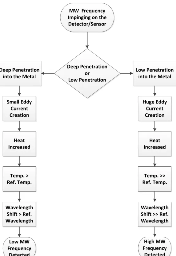
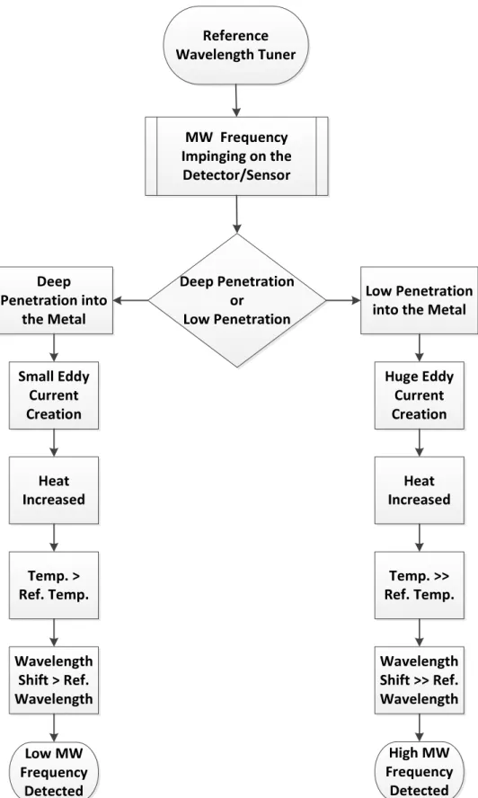
Creating SPR in optical fibers requires the use of a metal layer on the fiber. Microwaves (MW) can penetrate metal on the nanometer scale and can increase the heat in the metal.
Surface Plasmon Resonance
This part of the fiber core reflects the light of a specific wavelength and generally known as Fiber Bragg Grating (FBG). In another way, we can say that FBG is periodic wavelength scale variation of refractive index inscribed in the segment of the fiber core.
![Figure 1.2: Localized SPR when field (light) interacts with the plasmons [9].](https://thumb-ap.123doks.com/thumbv2/filepdfnet/10908237.0/14.892.211.684.329.607/figure-1-localized-spr-field-light-interacts-plasmons.webp)
SPR based Tilted Fiber Bragg Grating Sensor
Microwave Interaction with Metals
For the SPR-based optical fiber sensor, we usually use the metal film at the cladding layer to support the surface plasmon wave. Generally, the metal film used in the fiber sensor for SPR generation is gold (Au) or silver (Ag).
![Figure 3.3: Change in temperature of thin Au film with a thickness of 34.6 nm (left figure) and 29.5 nm (right figure) during microwave irradiation [67]](https://thumb-ap.123doks.com/thumbv2/filepdfnet/10908237.0/20.892.147.742.134.379/figure-change-temperature-thickness-figure-figure-microwave-irradiation.webp)
Microwave Detection Possibility
Experiment for Uniform FBG
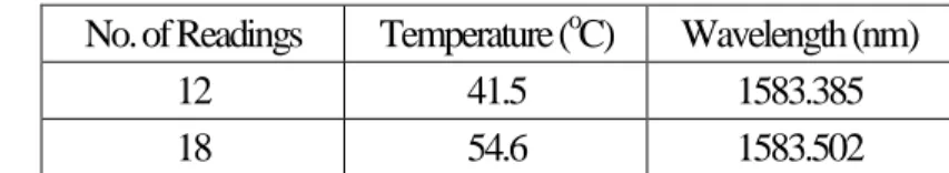
Experimental Data for Uniform FBG
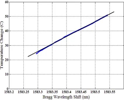
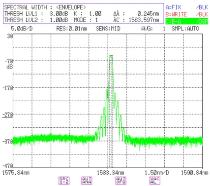
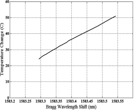
One of the observed Bragg shifted wavelengths in Optical Spectrum Analysis (OSA) is shown in Fig.
Calculation of Error for Uniform FBG
These parameters are the effective kernel index (neff ) and the grating period (Λ). When the temperature changes, the effective index also changes due to the thermo-optical effect, while the period changes due to the thermal expansion of the glass. As a result of the temperature change, the effective index changes by ∆neff and the grating period by ∆Λ, which will result in the overall Bragg wavelength change∆λB.
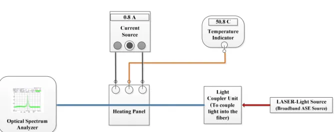
A power source to heat the panel was used (as we did earlier) where the CFBG was attached. The current was increased from 0A to 0.8A, resulting in the temperature increase of the panel from 27.7 0C to 54.6 0C respectively.
Experimental Data for Chirped FBG
4.6, linear fitting is performed by MATLAB and is presented together with an experimentally obtained curve of the Bragg wavelength dependence on temperature. If we pay more attention to the experimental curve, we can see that the measurements were not performed properly at the beginning, because in this area the dependence is not linear. Furthermore, the linear region starts from a temperature of 42 oC and ends at 55 oC.
From the above result, it is clear that the temperature response for the CFBG is linearly the same as the uniform FBG for a specific wavelength. From the experimental result, we can see that there is an average 6 pm wavelength shift due to 1 oC temperature change.
Calculation of Error for Chirped FBG
When MW affects the metal film of this type of sensor, the temperature of the metal film increases. By comparing the wavelength shift of the SPR wave with the reference wave (at room temperature), different MW frequencies can be detected. If we change the thickness of the metal layer, the sensitivity of the sensor will change as the SPR changes.
By comparing the wavelength shift of the SPR wave with the reference, we can detect the MW frequency. It is clear from the discussion that the thickness of the metal film is very important to observe the MW frequency. If we change the thickness of the metal layer, the sensitivity will also vary.
So, if we change the thickness of the metal layer, changing the SPR also changes the sensitivity of the sensor. More than the thickness of the metal will also affect the transmitted light [40]. The quality factor of the sensor also depends on the thickness of the metal film, as reported in [39].
Waveguide with SOI Material System
Eigenmodes of SOI Bent Waveguide
The neff of a circular bent waveguide was calculated as a function of the radius of the bend. The number of steps is chosen so that there are 15 steps (or more) inside the waveguide. The contrast between the refractive index of the waveguide and the index of the cladding must be clearly visible so that the mode in the waveguide will be limited, this means that we cannot choose the start and end values too far apart.
However, we must also leave part of the cladding surface (with a higher refractive index) in the simulation, because the program (simulator) uses this area to determine the losses. We expect the profile of the guided mode to be concentrated in the outer edge of the curved waveguide, because the mode is most strongly guided in the region with the highest refractive index. As the radius decreases, the mode will shift even more toward the outer edge of the waveguide.
Since the refractive index will be greater than the effective index of the waveguide mode at a certain distance from the bend, the effective index of a waveguide bending mode will be complex. After choosing the correct values for the parameters, we obtained neff as a function of the radius of the bend. Where R- radius, neff - effective index and k0 =2π λ. This formula also shows that when we are looking for a guided mode (with low losses), we need to find the mode that has the lowest imaginary index.
10 2log
Waveguide with SOS Material System
- Eigenmodes of SOS Bent Waveguide
After the same simulation (with different parameters) as we performed for SOI system, we obtained the values of neff, αφ and the loss as a function of the radius for SOS system. Assuming losses of up to 2dB/90° as we considered for SOI, the minimum radius of the bend is 2.5 mm for SOS system. Smaller bends cannot be made due to the low refractive index contrast between the core and the cladding.
Thus, we can say that if we change the lattice sections from lower to higher or vice versa, the reflective properties remain approximately the same. Therefore, from the above discussion, we can say that the reflection characteristic of CFBG is not completely dependent on the pitch size of the grating. The angle of inclination of the lattice plane with respect to the fiber axis must be taken into account.
The sensor characteristic also depends on the refractive index variation, the length variation of the FBG and the thickness of the gold layer. For better performance, we can coat the optical fiber of the sensor using anti-reflection coating (ARC) materials. To check the possibility of using ARC materials as coatings, we first consider the characteristic of ARC.
![Table 6.5: Effective index and loss as a function of the radius of the band for SOS Radius (µm) Re(n eff ) Im(n eff ) |n eff | α φ Loss [db/90°]](https://thumb-ap.123doks.com/thumbv2/filepdfnet/10908237.0/44.892.134.796.410.625/table-effective-index-loss-function-radius-radius-loss.webp)
Effect of ARC for SOI Material System
- Design & Simulation of AR Coating
- Result & Analysis .1 Without AR coating
- One layer AR coating
Finally they vary the thickness of the metal thin film, they used 40 nm, 50 nm and 60 nm and obtained instantaneous change in transmission peaks and wavelength shifts, in 46 mode the approximate transmission was 0.30 respectively. To maximize transmission for horizontal coupling, an anti-reflection coating can be placed on the sides of the chip. Table 7.1 gives the properties of this beam, σx and σy are the typical dimensions of the Gaussian function.
First, a single-layer coating is designed, then it is optimized, and finally, the design of a multi-layer coating is carried out using the Essential Macleod CAD tool. In Essential Macleod, we can only calculate the transmission through a stack of homogeneous layers, so we model the cross section of the waveguide structure with a single number, the neff effective index of the guided mode of the structure. CAD software allows us to calculate the transmission of plane waves incident at any angle, but the guided modes of waveguide structures are approximated by Gaussian rays (whose properties are given in Table 7.1).
We can solve this problem by decomposing the Gaussian beam into its plane wave components through spatial Fourier transform, calculating the transmission for each of these components, and then using the inverse Fourier transform to obtain the transmitted beam. The transmission through a layer stack is calculated, which is built up of a semi-infinite substrate layer (in this case the waveguide), a number of thin films and another semi-infinite medium (in this case air). These interference fringes surround the edges of the Gaussian beam because the beam width is small compared to the wavelength, causing diffraction.
21.74sin
Optimized one layer AR coating
Optimization of the coating was carried out by changing the thickness of the layer to increase the transmission.
Multi layer AR coating
So if we use the anti-reflective coating to maximize transmission; we get an average of 19%. The main concern is polarization, when there is no AR coating, the difference between TM polarized light transmission and TE polarized light transmission is high. Although AR coating reduces the polarization effect, TM polarized light transmission is always higher than TE polarized light.
This type of investigation can also be carried out for silicon dioxide on silicon (SOS) and other material systems to determine the optimized way of using AR coatings in terms of polarization and maximum light transmission.
Effect of ARC for SOS Material System
- Simulation
- Single Layer Coating Theoretical values for coating
- Optimized Single Layer Coating
- Multilayer Coating
No interference fringes around the edges of the Gaussian beam were observed because the beam width is large compared to the wavelength. The phase change is observed as a result of the interference of the different plane wave components of the Gaussian beam. This is because the beam width of the Gaussian beam is relatively larger compared to the wavelength, so the plane wave decomposition will be less spread out.
We optimized the transmission of the coating by varying the thickness of the coating using Simplex. The optimization leads to a thickness very close to the theoretical value and there is no change in the transmission values of the Gaussian beam. ARC materials must be a dielectric (such as MgF2) and must have a refractive index lower than the fiber core medium.
If it is possible to use ARC materials as cladding, the mode transmission through the cladding will be maximized due to less reflections. So the SPR will be higher and the sensor efficiency will increase. The SPR wave depends on various factors such as the thickness of the metal layer, polarization dependence, etc.
![Figure 2.1: Fiber Bragg Grating, refractive index modulation and spectral response [10]](https://thumb-ap.123doks.com/thumbv2/filepdfnet/10908237.0/16.892.167.720.133.359/figure-fiber-bragg-grating-refractive-modulation-spectral-response.webp)
![Figure 3.4: Microwave effect on Au film with different thicknesses T1=45 nm, T2=133 nm & T3=407 nm (a) for H-field (b) for E-field [34]](https://thumb-ap.123doks.com/thumbv2/filepdfnet/10908237.0/20.892.140.740.741.973/figure-microwave-effect-film-different-thicknesses-field-field.webp)