DESIGN OF 240V SQUARE WAVE INVERTER
HARTINI BINTI ABDUL HAMID
HARTINI BINTI ABDUL HAMID
This Report Is Submitted In Partial Fulfillment Of Requirements For The Degree of Bachelor In Electrical Engineering (Power Electronic and Drives)
FACULTY OF ELECTRICAL ENGINEERING UNIVERSITI TEKNIKAL MALAYSIA MELAKA
“I hereby declared that I have read through this report and found that it has comply the partial fulfillment for awarding the degree of Bachelor of Electrical Engineering
(Power Electronic and Drives).”
Signature : ………
Supervisor’s Name : ……….
“I hereby declared that this report is a result of my own work except for the excerpts that have been cited clearly in the references..”
Signature : ………
Name : ………..
iii
ACKNOWLEDGEMENTS
Throughout the completing this PSM 2, a lot of experience had I gained in writing this documentation. Hence, I would like to express my appreciations to everyone that have contributed towards the success my PSM 2.
I would like to take this opportunity to thank my supervisor, Mr. Saifulza Bin Alwi and Mr. Azzidin for his patience help, advice, full attention, encouragement and professionalism throughout the time. They are very kind and patience lecturer who tolerated from the beginning of the document to the completion. Thank you.
It is therefore difficult to name all the people who have directly or indirectly helped me in this effort; an idea here and there may have appeared insignificant at the time but may have had a significant causal effect. However, special thanks must first go to my family, who over the duration has been neglected even ignored, during my deepest concentrations.
v
ABSTRACT
ABSTRAK
vii
TABLE OF CONTENTS
CHAPTER SUBJECT PAGE
DECLARATION ii
DEDICATION iii
ACKNOWLEDGEMENTS iv
ABSTRACT v
ABSTRAK vi
TABLE OF CONTENTS vii
LIST OF FIGURES ix
LIST OF ATTACHMENTS xi
I INTRODUCTION
1.1 Introduction 1
1.2 Problem Statement 6
1.3 Objectives 7
1.4 Scope 7
1.5 Expected Output 7
II LITERATURE REVIEW
2.1 Introduction 8
2.2 Introduction to Inverter 9
2.2.1 Dc-Dc Converter 11
2.2.2 Filtering 13
2.2.3 Harmonic Filtering 14
2.3 Conventional Inverter 15
2.5 Application of Inverter in Practical 20
2.6 MOSFET 21
2.7 IC SG3526 22
2.8 OptoCoupler (HCPL3150) 23
2.9 Software Pspice 24
2.9.1 Orcad PSpice 9.1 25
2.9.2 Single Phase Uncontrolled 26 Bridge Rectifier
2.10 Circuit Diagram 27
III METHODOLOGY
3.1 Project Methodology 30
IV CIRCUIT ANALYSIS
4.1 Quasi Square Wave Inverter Signal Circuit 32
4.2 DC Power Supply 34
4.3 Dead Time Circuit and Optocoupler Circuit 35
4.4 Operation Circuit 38
V RESULT
5.1 Quasi Square Wave Inverter Calculation 39
5.2 Theoretical Calculation 40
5.3 Simulation Result 40
5.4 Experimental Result 47
5.4.1 Hardware Part Simulations 49 5.4.2 Signal Generation Circuit 49 5.4.3 PWM Generation Circuit 51
VI CONCLUSION AND RECOMENDATION 57
ix
LIST OF FIGURES
NO TITLE PAGE
1.1 General Block diagram 1
1.2 Equivalent circuit 2
1.3 Modified Sine Wave 4
1.4 Modified sine wave and true sine wave 5
2.1 Basic diagram 8
2.2 Block diagram 9
2.3 Harmonics filtering of inverter 13
2.4 Conventional Voltage Source Inverter (VSI) 15
2.5 Basic block for quasi square inverter 16
2.6 Shoot through fault 18
2.7 Dead-time 18
2.8 Regulated inverters 19
2.9 Whole Operation of Inverter 20
2.10 MOSFET (1) 22
2.11 Construction 3526 23
2.12 An Optocoupler Symbol or Schematic 24
2.13 Software PSPICE 25
2.14 Orcad Capture CIS project window 26
2.15 PSpice Simulation Setting 26
2.16 Circuit Diagram for DC Supply Voltage 27
2.17 Dead Time Circuit and Gate Drive 28
2.18 Quasi Square Wave Signal Circuit 29
2.19 MOSFET control circuit 29
3.1 Diagram of Project Methodology 31
4.1 Circuit for SG3524 34
4.2 DC Power Supply Circuit 34
4.4 Circuit for HCPL3150 37
4.5 Circuit for Inverter (MOSFET) 37
4.6 Hardware Development 38
5.1 Circuit diagram for α = 90˚ 43
5.2 Result for α = 90˚ 43
5.3 Circuit diagram for α = 35.98˚ 44
5.4 Result for α = 35.98˚ 44
5.5 Circuit diagram for α = 162˚ 45
5.6 Result for α = 162˚ 45
5.7 Circuit diagram for α = 180˚ 46
5.8 Result for α = 180˚ 46
5.9 DC Power Supply Simulation 48
5.10 Wave form DC Power Supply 48
5.11 Signal Generation circuit 50
5.12 Output of Signal Generation circuit 50
5.13 PWM Generation circuit 51
5.14 PWM Output 51
5.15 Output for pin CT 52
5.16 Output A 52
5.17 Output B 53
5.18 Output from PWM signal 53
5.19 Pulse signal with 50 Hz frequency generated by SG3524 54 5.20 Pulse signal with different frequency (80 Hz) 54
5.21 Pulse signal with different duty cycle 55
5.22 Wave Input from IC7804 55
5.23 Output from HCPL 3150 56
xi
LIST OF ATTACHMENTS
APPENDIX TITLE PAGE
A Data sheet (SG3526) 60
B Data sheet (LM78XX) 66
C Data sheet (LM79XX) 69
D Data sheet (IN4749A) 72
E Data sheet (7408) 74
F Data sheet (7414) 78
G Data sheet (HCPL3150) 82
CHAPTER 1
INTRODUCTION
1.1 Introduction
Inverter is a dc-to-ac converter. The function of an inverter is to change a dc input voltage to a symmetric ac output voltage of desired magnitude and frequency like the general block diagram shown at figure 1.1 below. Depending on the input dc voltage range in comparison to the output ac voltage, inverters also can be buck inverters, boost inverters, or buck-boost inverters. The applications of the inverter are power conversion from variable dc voltage into fixed ac voltage for stand-alone applications or ac current output following the grid voltage and frequency for grid-connected applications.
[image:14.595.207.433.492.600.2]Figure1.1 General Block diagram of Inverter
2
Figure1.2 Equivalent circuit
Inverters are widely used in industrial applications such as: a. variable-speed ac motor drives
b. induction heating c. traction
d. standby power supplies e. uninterruptible power supplies
The input may be a battery, fuel cell, solar cell or other dc source. Inverters can be broadly classified into two types;
a. single phase inverters b. three phase inverters
Each type can be controlled by turn-on and turn-off devices such as: a. MOSFET (metal oxide semiconductor field-effect transistors) b. IGBT (insulated-gate bipolar transistors)
c. BJT (bipolar junction transistor)
d. MCT (metal-oxide semiconductor-controlled thyristor) e. SIT (static induction transistor)
f. GTO (gate-turn-off thyristor)
modified sine-wave (quasi sine wave) and true sine-wave. Square wave inverters are largely outdated, as the waveform shape is not well suited for running most modern appliances, and prices have come down considerably for the superior modified sine wave and true sine wave types running some type of electrical tools and motors and incandescent lights.
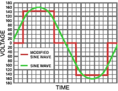
Modified Sine Wave Inverters is designed to have characteristics similar to the sine wave shape of utility power. A waveform of this type is suitable for most AC loads, including linear and switching power supplies used in electronic equipment, transformers, and motors. This waveform is much better to the square wave produced by many other dc to ac inverters. The least expensive type of modern inverter produces modified sine wave power. The waveform looks like a stair-step, where the power rises straight from zero to upper peak voltage, straight back to zero, and straight to lower peak voltage, resting at each point for a moment.
Modified sine wave inverters will run many household appliances such a televisions, radios, washers, dryers and microwaves (or some that use electronic timing for cycling) with occasional minor electrical "noise" present. The quasi square wave inverter is inherently smaller, simpler and more reliable and efficient than the sine wave inverter. The only apparent disadvantage is a 3 to 5 percent loss in motor efficiency and the performance degradation. Variations in induction motor performance may occur when a motor is driven from a quasi square wave inverter rather than a sine wave source. It will use about 20% more power with a modified sine wave than with a true sine wave. The performance difference may be a change in speed, maximum torque or maximum power capability depending on the motor power factor and inverter configuration.
4
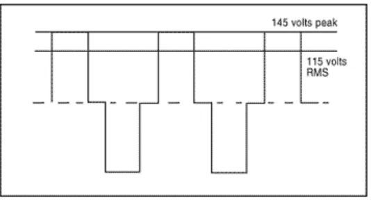
Figure 1.3: Modified Sine Wave
The power supplied by utility companies and engine generators is a true sine wave form. This is the most reliable waveform for household use. True sine wave power passes from the upper and lower peak voltages in a smooth curved wave, rather than the stair-step of the modified sine wave. All appliances and electronic equipment will run as intended when using sine wave power. True sine wave inverters will produce AC power as good as or better than utility power, ensuring that even the most sensitive equipment will run properly. While sine wave inverters are more expensive than modified sine wave models which shown as figure 1.3 above, the quality of their waveform can be a definite advantage.
Figure 1.4: Modified sine wave and true sine wave
A dc-ac converter is a circuit that converts the dc voltage supply to an ac voltage output and this converter also known as inverter. The function of an inverter is to change a dc input voltage to a symmetric ac output voltage of desired magnitude and frequency.
This project is to design Quasi Square Wave Inverter that supply 240 Vac which controlled by four switches of MOSFET (Metal Oxide Semiconductor Field Effect Transistor). The MOSFETs also are controlled by gate drive circuits.
Inverter is used in many types of industrial and commercial applications especially in dc–ac conversion, ac motor drives, system controls and Uninterruptible Power Supply (UPS).
This project will include operation, analysis, control strategy and experimental result based on the software and hardware implementation.
1.2 Problem statement
6 is approximately half than a low frequency transformer. Therefore, it can replace the 240 V DC power supplies that had being used in this project which is larger in size and weight.
There should be a feedback controller for this inverter circuit. It is very useful in practical because in real situation, the power output will always changing with the change of load. When the load is changing then the output voltage will also change. Therefore this feedback controller circuit will regulate the dc input voltage to the inverter in order to fix it at the required voltage.
The quasi square wave output waveform has to be changed with the sine wave because in most application a pure sine wave output is required. Therefore the switching scheme at the inverter drive circuit has to be changed with the PWM (Pulse Width Modulating) switching scheme.
Quasi square waveform is inherently generated in a three-phase inverter bridge by switching the transistors on and off at the proper intervals therefore, the resulting inverter is smaller, lighter weight, and simpler, implying greater reliability and lower cost. These advantages invite a closer look at inverter-motor systems, particularly for space flight. The only apparent disadvantage is a 3 to 5 percent loss in motor efficiency and the performance degradation discussed later. Methods to eliminate the performance degradation, which depends somewhat on the switching drive to the bridge transistors, are discussed, and test results are presented.
The objectives of this project are:
a) Develop a quasi square wave inverter and analysis the circuit. b) Build in small size and weight.
c) Upgrade the present hardware of a quasi square wave inverter by using dead time circuit, gate drive circuit and (MOSFET). d) Calculate the theoretical values of inverter and compare it with
simulation result.
e) Simulate the circuit using OrCad software and develop the hardware circuit.
1.4 Scope
The construction of this project will use full bridge inverter which is converting input voltage of 24Vdc to output voltage of 240Vac. The inverter designed will consists of dc power supplies circuit, dead time circuit, step up transformer, and gate drive circuit. Analyses of quasi square wave inverter performance and characteristic.
1.5 Expected Output
At the end of this project, overall size of the circuit in this project is quite small while the gate drive circuit diodes are connected in anti-parallel with the switches a distinction must be mode between the on states versus the conducting state of the switch.
8
CHAPTER 2
LITERATURE REVIEW
2.1 Introduction
[image:21.595.110.527.442.663.2]The chapter describes about literature review. A literature review is an evaluate report information found in the literature research to the related area of study. The literature review part will describe domain related with the project and existing system that related to the project. Figure 2.1 and figure 2.2 below shows basic diagram for whole operation and block diagram of inverter.
Figure 2.2: Block diagram of inverter
2.2 Introduction to Inverter
The output voltage could be fixed or variable at a fixed or variable frequency. A variable output voltage can be obtained by varying the input dc voltage and maintaining the gain of the inverter constant. If the dc input voltage is fixed and it is not controllable, a variable output voltage can be obtained by varying the gain of the inverter, which is normally accomplished by pulse-width modulation (PWM) control within the inverter. The inverter gain may be defined as the ratio of the ac output voltage to the dc input voltage.
There are three inverter types:
1. Voltage Source Inverter (VSI) – creates an ac voltage and current from a dc voltage source
2. Current Source Inverter (CSI) – creates an ac voltage and current from a dc current source
3. Resonant Inverter – the load is involved in a series resonant circuit in order to produce a high frequency sine wave ac voltage
Power Supply 24Vdc
Inverter Filter Transformer Output
240Vac
10 If the output voltage or current of the inverter is forced to pass through zero by creating an LC resonant circuit, this type of inverter is called resonant-pulse inverter and it has wide applications in power electronics.
The Voltage Source Inverter (VSI) is divided into three general categories:
1. Pulse-width-modulated inverter
The input dc voltage is essentially constant in magnitude. A diode rectifier is used to rectify the line voltage. Therefore the inverter must control the magnitude and frequency of the ac output voltages. This is achieves by PWM of the inverter switches and hence such inverters are called PWM inverters. PWM provides a way to decrease the Total Harmonic Distortion (THD) of load current. This method generally meet THD requirement more easily than the square wave switching scheme. The unfiltered PWM output will have relatively high THD but the harmonics will be at much higher frequencies than for a square wave, making filtering easier. In PWM, the amplitudes of the output voltage can be controlled with the modulating waveforms. Control of the switches for PWM output requires:
a. a reference / modulating / control signal
b. carrier signal (triangular wave that controls the switching frequency)
The advantages of PWM are:
a. reduction in filter requirements to decrease harmonics b. easier to control the output voltage amplitude
The disadvantages of PWM are:
a. complex control circuit for the switches b. losses increase due to more frequent switching
2. Square-wave inverters
The dc input voltage is controlled in order to control the magnitude of the output ac voltage. Therefore the inverter has to control only the frequency of the output voltage. The output ac voltage has a waveform similar to a square wave so these inverters are called square-wave inverters.
magnitude and the frequency of the inverter output voltage, even though the output to the inverter is a constant dc voltage and the inverter switches are not pulse-width modulated (and hence the output voltage wave shape is like a square wave). Therefore this inverter combines the characteristics of the previous two inverters. The voltage cancellation technique works only with single-phase inverters and not with three-phase inverters. Mainly three Voltage Source Inverter circuit topologies are used:
1. Full Bridge Inverter - most powerful circuit. The voltage across the transistor is equal to supply voltage. The load could be ac supplied via transformer
2. Half Bridge Inverter - circuit uses the half of dc supply voltage. Hence, its output voltage and power are twice less than compared to other circuits Push Pull Inverter - allows easy transistor driving but requires a transformer and transistor voltage is twice higher. The output voltage depends on transformer ratio
2.2.1 Dc-Dc Converter
In many industrial applications, it is required to convert a fixed-voltage dc source into a variable-voltage dc source. A dc-dc converter converts directly from dc to dc and is simply known as a dc converter. Dc converters are widely used for traction motor control in electric automobiles, trolley cars, marine hoists, forklift trucks and mine haulers. They provide smooth acceleration control, high efficiency and fast dynamic response. Dc converters are used in dc voltage regulators and also are used in conjunction with an inductor to generate a dc current source especially for the current source inverter.