UNIVERSITI TEKNIKAL MALAYSIA MELAKA
EFFECT OF ELECTRICAL GROUNDING OF SUBSTRATE ON
THE MAGNETRON SPUTTERING OF TITANIUM FILM
This report submitted in accordance with requirement of the Universiti Teknikal Malaysia Melaka (UTeM) for the Bachelor Degree of Manufacturing Engineering
(Engineering Materials) (Hons.)
by
MOHD NABIL FIKRI BIN HANIF
B050910187
880207085039
UNIVERSITI TEKNIKAL MALAYSIA MELAKA
BORANG PENGESAHAN STATUS LAPORAN PROJEK SARJANA MUDA
TAJUK: Effect of Electrical Grounding of Substrate on the Magnetron Sputtering of Titanium Film
SESI PENGAJIAN: 2012/ 2013 Semest er 2
Saya MOHD NABIL FIKRI BIN HANIF
mengaku membenarkan Laporan PSM ini disimpan di Perpust akaan Universit i Teknikal Malaysia Melaka (UTeM) dengan syarat -syarat kegunaan sepert i berikut :
1. Laporan PSM adalah hak milik Universit i Teknikal Malaysia Melaka dan penulis. 2. Perpust akaan Universit i Teknikal Malaysia Melaka dibenarkan membuat salinan unt uk
t uj uan pengaj ian sahaj a dengan izin penulis.
3. Perpust akaan dibenarkan membuat salinan lapor an PSM ini sebagai bahan pert ukaran ant ara inst it usi pengaj ian t inggi.
SULIT
TERHAD
TIDAK TERHAD
(Mengandungi maklumat yang berdarj ah keselamat an at au kepent ingan Malaysiasebagaimana yang t ermakt ub dalam AKTA RAHSIA RASMI 1972)
(Mengandungi maklumat TERHAD yang t elah dit ent ukan oleh organisasi/ badan di mana penyelidikan dij alankan)
Alamat Tet ap:
DECLARATION
I hereby, declared this report entitled “Effect of Electrical Grounding of Substrate on the Magnetron Sputtering of Titanium Film” is the results of my own research except as cited
in references.
Signature :……….
Author’s Name : MOHD NABIL FIKRI BIN HANIF
APPROVAL
This report is submitted to the Faculty of Manufacturing Engineering of UTeM as a partial fulfillment of the requirements for the degree of Bachelor of Manufacturing Engineering B.ENG. (HONS) (Engineering Materials). The member of the supervisory is as follow:
………
(Principal Supervisor)
………
ABSTRACT
Property of thin film depends on the voltage bias that applied to the depositing substrate during the D.C. magnetron sputtering process. . This shows ionized atoms or molecules are involved in deposition of film to the substrate. The supposed accumulation of charges (ions) on the surface of substrate may affect the deposition of the incoming ionized atom or molecules because like-changes exert repulsive electric force. Improvement of electrical grounding of substrate used for the deposition of Ti film may help to reduce the charge accumulation on the surface of substrate. The reduction of the accumulated charges on the substrate may decrease the repulsion effect on incoming ionized sputtered atoms and increases the deposition rate of sputtered atoms on the substrate. The effect on the Ti film may be exhibited through the microstructure and phase composition of the film. Electrical grounding condition of depositing substrate during Ti film deposition will be varied using different: (1) Design of substrate holder, (2) substrate material, and (3) coating thickness linking substrate with substrate holder. Obtained Ti films were characterized using were characterized with optical microscopy, SEM, and electrical resistivity measurement.
ABSTRAK
Sifat-sifat filem nipis bergantung kepada kadar voltan yang dikenakan ke atas substrat deposit semasa proses pemercikan DC dilakukan. Ia menunjukkan atom terion atau molekul berlaku dalam pemendapan filem substrat. Pengumpulan caj (ion) pada kebiasaannya terjadi di permukaan substrat boleh menjeaskan pemendapan atom terion atau molekul yang masuk kerana perubahan yang daya elektrik yang dikenakan ditolak.
Peningkatan asas elektrik substrat digunakan untuk pemendapan Ti filem boleh membantu untuk mengurangkan pengumpulan caj di permukaan substrat. Pengurangan caj terkumpul pada substrat boleh mengurangkan kesan penolakan atom yang terion pada pemercikan atom dan meningkatkan kadar pemendapan pemercikan atom pada substrat. Kesan ke atas filem Ti itu boleh dipamerkan melalui mikrostruktur dan fasa komposisi filem. Keadaan asas elektrik pemegang substrat semasa Ti filem pemendapan akan diubah yang digunakan berbeza iaitu: (1) Bentuk pemegang substrat, (2) Bahan-bahan substrat, dan (3) Ketebalan lapisan substrat yang dihubungkan dengan pemegang substrat. Merujuk kepada Ti filem, pengujian sifat-sifat Ti filem dilakukan dengan menggunakan mikroskop optik, Scanning Elecktron Microscopy (SEM), dan pengukuran rintangan elektrik ke atas substrate.
DEDICATION
“Special to my parents, my family and all my friends that helps me in finishing this research”.
ACKNOWLEDGEMENTS
In the Name of Allah, the Most Gracious, the Most Merciful.
Alhamdullilah, be thanks to Allah S.W.T because of blessing I can finish this research. I wish to acknowledge the contribution of my parents for their continued support and understanding during the research of microstructural characterization of corrosion product for natural gas pipelines in Malaysia. Special thanks should also go to my supervisor Prof. Dr. Mohd Razali Mohamad and my adviser Dr. Lau Kok Tee and staffs at Universiti Teknikal Malaysia Melaka (UTeM) for their help me in finishing this research. Not to forget all lecturers, technicians, friends in UTeM for their help and full cooperation to finishing my research.
Lastly, I’m happy to present the following cumulative list of all those individuals who, in one way or another, made various contributions to this research.
TABLE OF CONTENTS
2.5 Parameter Controlling PVD DC Magnetron Sputtering 19
2.5.1 Substrate Bias Voltage 19
2.5.2 Sputtering Power 21
2.5.3 Substrate temperature 21 3.4.3 Coating thickness between substrate to holder (conduction path) 34
3.5 Characterization 35
3.5.1 Optical Microscope (digital image) 35 3.5.2 Scanning Electron Microscope (SEM) and Energy Dispersive X-ray
Spectroscopy 35
3.5.3 Resistivity on Voltmeter 39
4.0 RESULT AND DISCUSSION 41
4.1 Optical Microscopic Image of Surface of Ti-coated Substrate 41 4.1.1 Coating thickness view of digital image 41 4.1.2 Surface Colour of Ti-Coating deposited using Different Holder Design 43
4.1.2.1 Effect of Original Holder and Springy Holder’s Design on Surface
Colour of Ti-coated Aluminium 43
4.1.2.2 Effect of Original Holder’s and V-flat Holder’s Design on Surface
Colour of Ti-coated Glass 44
4.2 Scanning Electron Microscope (SEM) Image 46 4.2.1 Cross Section of Ti-coated Glass Deposited at Different
Coating Time 46
4.2.2 Surface structure of Ti-coated Glass 48 4.3Energy Dispersive X-ray Spectroscopy (EDX) 50
4.5 Electrical Resistivity of Ti Film 52
5.0 CONCLUSION AND RECOMMENDATION 56
5.1 Conclusion 56
5.2 Electrical Resistivity of Ti Film 58
REFERENCES 59
APPENDIX
A GANT CHART
LIST OF FIGURES
No. Figures Caption Page
2.1 Crystal structures of Titanium 6
2.2 Crystal structure of rutile and anatase phases of TiO2 8
2.3 Phase diagram of Ti-O system the region Ti2O3 – TiO2 contains
Ti2O3, Ti3O5, seven discrete phases of homologous series TinO2n-1
(Magneli phases) and TiO2.
10
2.4 Schematic diagram of radio frequency planar DC magnetron 13
2.5 The principle of sputtering process 18
2.6 Example affect Substrate Bias Voltage 20
2.7 Thornton Model 22
2.8 Illustration of electrical flow in PVD 24
3.1 Methodology Sequence 26
3.2 KOREA VAC-TEC PVD model VTC 1000 and substrate holder inside coating chamber
28
3.3 Ultrasonic bath cleaner model JAC1505 28
3.4 Illustrate of DC magnetron sputtering process 31
3.5 Substrate holder for PVD magnetron sputtering 38
3.6 Illustration of contact between substrate holder and substrate. i) Alligator clip holder design (original holder), ii) Flat (modified) and iii) Flat surface clip holder design – steel (modified).
33
3.7 Illustration of coating thickness on the substrate to holder (conduction path)
34
3.8 Signal produced when electron beam interact to the sample 37
3.9 Evo 50 series apparatus 37
3.10 Equipment setup for SEM and EDX 38
3.11 Illustration of resistivity testing on the samples 40
4.1 Sample of Ti film on the aluminum substrate for 45, 60, 75 minutes 42 4.2 Sample of Ti film on the mild steel substrate for 60 minutes
(Original)
43
4.3 Sample of Ti film on the mild steel substrate for 60 minutes (Springy)
44
4.4 Sample of Ti film on the glass substrate for 60 minutes (Original) 45 4.5 Sample of Ti film on the glass substrate for 60 minutes (V-flat) 45 4.6 Sample thickness of Ti film on the glass substrate for 45 minutes 47 4.7 Sample thickness of Ti film on the glass substrate for 60 minutes 47 4.8 Sample thickness of Ti film on the glass substrate for 75 minutes 48 4.9 Sample surface of Ti film on the glass substrate for 45 minutes 48 4.10 Sample surface of Ti film on the glass substrate for 60 minutes 49 4.11 Sample surface of Ti film on the glass substrate for 75 minutes 49 4.12 The Spectroscopy data of glass substrate specimen 50
LIST OF TABLES
No. Tables Caption Page
2.1 Crystal Structure for Titanium Dioxide (TiO2) 8
3.1 Specification data for PVD coating machine 30
3.2 Properties of difference substrate material 32
3.3 Specification Data for SEM 36
3.4 Specification of scanning electron microscopic 37
4.1 The elements analysed of glass substrate specimen 51 4.2 Value of resistivity on glass, mild steel and aluminium substrate
based on the time of coating
53
4.3 Value of resistivity on glass, mild steel and aluminium substrate based on the types of holder
54
5.1 Over all of the behaviour of deposit Ti Film coating with changes PVD process parameters
57
NaCl - Sodium Chloride
SEM - Scanning Electron Microscope
T - Temperature
Ta - Tantalum
Ti - Titanium
TiO2 - Titanium Dioxide
Ts - Substrate Temperature
T/Tm - Thorton Model unit
UTeM - Universiti Teknikal Malaysia Melaka
CHAPTER 1
INTRODUCTION
Chapter 1 will give a brief explanation about this project, starting with the background of the project title, “Effect of electrical grounding of substrate on the magnetron sputtering of titanium film”. This chapter will also discuss about the problem statement, the objective and the scope and limitation of this project.
1.1 Background
Nowadays, the technique of deposition of thin film by physical vapor deposition (PVD) has been used widespread in many industrial sectors. This technique is used for a variety of field coating application such as metalworking industry, biomedical application and optical or electrical component. High hardness, wear and corrosion resistance, low friction, and specific optical of electrical properties and decorative color and often complex combination of properties are the reasons about increasing demand in the industry. Magnetron sputtering for thin film process is one of the technology that developed by PVD. It’s the one of choice for deposition of a wide range of industrially important coating. Theoretically, this process allows deposition of metal, alloy, ceramic, and polymer thin film into any substrate material. Sputtering, also known as sputter etching, is used for patterning semiconductor wafers, for cleaning surfaces, for micromachining, depth profiling, and a number of applications which require careful, microscopic erosion of a surface. Sputter deposition is used for film deposition on semiconductor wafers, on magnetic media and head surfaces, for coating tools and cutting surfaces for wear resistance (this includes, by the way, such tools as shaving razors), for reflective coatings on window glass, for coating the insides of plastic bags and the
surfaces of automobile parts, and a number of other wide ranging applications. Sputtering is usually practiced by means of plasmas which generate charged particles which can be accelerated towards a surface electrically. Sputtering is simply the process of erosion of that surface by the energetic particles, a sort of atomistic sandblasting. Sputter deposition is nothing more than the accumulation of these atoms which are blasted off the surface onto a nearby sample. For the most part, this chapter deals with sputtering and sputter deposition with a slant towards semiconductor processing. However, the discussion is wide enough that other areas are introduced from time to time as needed.
1.2 Problem Statement
The Ti film fabricated by many techniques such as reactive sputtering in PVD, sol-gel coating, atomic layer deposition and etc. the microstructure, crystallographic texture, state of stress and chemical compound are influenced by particle bombardment of the growing film, deposition temperature, and composition of elements in the coating material. However there are other parameters that may contribute to the characteristic of the Ti thin film.
Electrical grounding of the substrate during deposition of the Ti film may help to reduce the charge accumulation on the surface of substrate. These suggest that electrical grounding of the substrate may affect the deposition of Ti film. Its effect may be exhibited through the microstructure and phase composition of the film. Property of thin film depends on the voltage bias that applied to the substrate. When voltage is increased on thin film shows the higher hardness and compressive stress value on microstructure. This shows ionized atoms or molecules are involved in deposition of film to the substrate. The supposed accumulation of charges (ions) on the surface of substrate may affect the deposition of the incoming ionized atom or molecules then this may affect the microstructure and phase composition of the deposited thin film.
In order to solve the problem, this project will study either the electrical grounding effect towards the process. The study must be considered about testing the different type of thin film and different voltage apply to substrate holder.
1.3 Objectives
The objectives to be achieved at the end of this project are as below:
i. To synthesize the titanium thin film on the substrateS using Direct Current (DC) sputtering technique.
ii. To study the effect of the electrical grounding of the substrate on the microstructure and phase composition of the deposited titanium dioxide thin film.
iii. To compare the differences in the effect between all of the substrates
1.4 Scope
This project will determine the effect of electrical grounding on the substrate during deposition of Ti. Three main factors that influence the electrical grounding of the substrate has been identified and they are:
i. Conductivity of substrate and coating material ii. Physical contact between substrate and holder
iii. Coating thickness on a substrate - holder which form a conduction path between substrate and holder.
The titanium oxide is selected as a target in DC magnetron sputtering. The effect electrical grounding is identified by using three types of tester and they are the optical image by using a microscope, thickness and surface morphology changing by using Scanning Electron Microscope and the value of the resistivity effect of the film coated on substrates. After the result has shown, it will compare together to see either the result shows the grounding is one of critical parameters or wisely.
CHAPTER 2
LITERATURE REVIEW
This chapter will explain about all elements used for this report. First explanation will come to machine, machine process, material (specimen) and process sequences for magnetron sputtering in order to know the element used and identify the parameter appear toward the study. The studies also related about analyzing the structure of the specimen after sputtering process.
2.1 Ti properties and applications
Titanium (Ti) is a lustrous transition metal with a silvery-gray color, high strength and low density. It is a chemical element and the number of atomic is 22. To produce strong lightweight alloys, titanium usually can be alloyed with iron, aluminum, vanadium, and many more among others element. In coating, titanium is nearly as resistant to corrosion as platinum, and resists many salt solutions, acids and even chlorine gas. It is also not water soluble, save perhaps in concentrated acids. Titanium is nonmagnetic and has good heat-transfer properties. Its coefficient of thermal expansion is somewhat lower than that of steel and less than half that of aluminum. Titanium and its alloys have melting points higher than those of steels. Titanium has the ability to passively and thereby exhibits a high degree of immunity to attack by most mineral acids and chlorides.
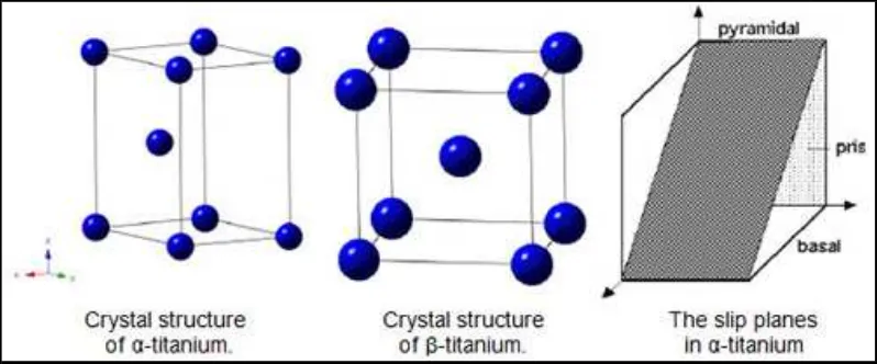
The crystal structure of titanium at ambient temperature and pressure is close-packed
hexagonal (α) with ac/a ratio of 1.587. Slip is possible on the pyramidal, prismatic and basal
planes in the close-packed directions. At about 890°C, the titanium undergoes an allotropic transformation to a body-centered cubic β phase which remains stable to the melting temperature (Figure 1).
Figure 2.1: Crystal structures of Titanium
Titanium is a remarkable, very light metal with a silvery color and is the fourth most abundant element in the earth’s crust. As a rule, all ignoble metals are extracted as a metal oxide. The lower the position of the standard potential of the metal in the nobility table, the more difficult it becomes to separate the metal from the bound oxygen. Iron has a potential of -0.44 volts and can be quite easily separated from the bound oxygen. This can be represented
by the reduction formula 2FeO + C + e 2Fe + CO2 furnace, and the “e” in the formula stands for the energy that needs to be added to make this
reduction possible.
If one adapts this mechanism to titanium oxide, also called rutile, nothing happens, since titanium oxide must be treated very differently in order to separate these two strongly bound elements.
This process is as follows:
1. Rutile (TiO2) is chlorinated with cokes to produce titanium tetrachloride (TiCl4) and carbon dioxide (CO2). Titanium tetrachloride is a colorless liquid that remains to be refined.
2. Magnesium or sodium is added to the titanium tetrachloride in an inert environment. 3. This produces the chemical reaction TiCl4 + 2Mg2+ Ti + 2MgCl2. Finally, we obtain
titanium sponge and magnesium chloride.
4. The titanium sponge is pressed into blocks and melted under inert gas to form ingots, to which alloy elements and scrap may be added. These ingots are then rolled to produce all kinds of half-finished products such as sheets or rods.
It will by now be clear that it takes a lot of energy to win titanium from its ore. This has to do with the fact that it takes a lot of energy to prepare magnesium or sodium. Therefore a large part of the price of titanium is determined by energy prices (Stepanov, 2011).
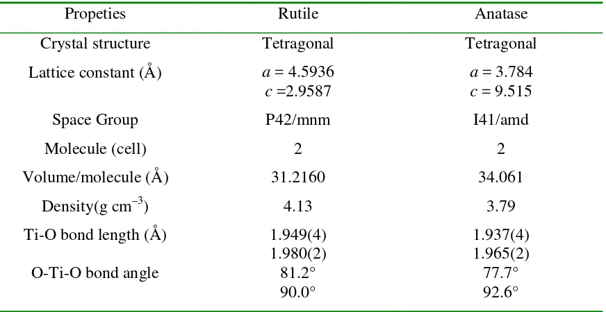
TiO2 belongs to the family of transition metal oxides. There are four commonly known
polymorphs of TiO2 found in nature: anatase (tetragonal), brookite (orthorhombic), rutile
(tetragonal), and TiO2 (monoclinic). Besides these polymorphs, two additional high-pressure
forms have been synthesized from the rutile phase (Stepanov, 2011).
In this review, only the crystal structures (Table 1) and properties of the rutile and anatase polymorphs are considered.
Table 2.1: Crystal Structure for Titanium Dioxide (TiO2) (Stepanov, 2011).
Propeties Rutile Anatase
Crystal structure Tetragonal Tetragonal
Lattice constant (Å) a = 4.5936 c =2.9587
a = 3.784 c = 9.515
Space Group P42/mnm I41/amd
Molecule (cell) 2 2
Volume/molecule (Å) 31.2160 34.061
Density(g cm–3) 4.13 3.79
Figure 2.2: Crystal structure of rutile and anatase phases of TiO2 (Stepanov, 2011).
Rutile TiO2 has a tetragonal structure and contains 6 atoms per unit cell. The TiO6 octahedron
is slightly distorted. The rutile phase is stable at most temperatures and pressures up to 60 kbar, where TiO2 becomes the thermodynamically favorable phase. anatase structures
transformed to the rutile phase after reaching a certain particle size, with the rutile phase becoming more stable than anatase for particle sizes greater than 14 nm. Once the rutile phase formed, it grew much faster than the anatase. The activity of the rutile phase as a photocatalyst is generally very poor. However, the rutile phase can be active or inactive, depending on its preparation conditions (Yingyot, 2008).
Anatase TiO2 also has a tetragonal structure but the distortion of the TiO6 octahedron is
slightly larger for the anatase phase, as depicted in Figure 1. The anatase phase is more stable than the rutile at 0 K, but the energy difference between these two phases is small (∼2 to 10 kJ/mol). The anatase structure is preferred over other polymorphs for solar cell applications because of its higher electron mobility, low dielectric constant and lower density. The increased photoreactivity is because of the slightly higher Fermi level, lower capacity to adsorb oxygen and higher degree of hydroxylation in the anatase phase. The reactivity of (001) facets is greater than that of (101) facets in an anatase crystal. Uniform anatase crystals containing 47% (001) facets using hydrofluoric acid as a morphology controlling agent (Stepanov, 2011).