i
DESIGN OF A LOW NOISE AMPLIFIER FOR 5-6GHz APPLICATIONS
NUR DIYANA BINTI ISMAIL
This Report Is Submitted In Partial Fulfillment Of Requirements For The Bachelor Degree of Electronic Engineering (Telecommunication Electronic) with honours
Fakulti Kejuruteraan Elektronik dan Kejuruteraan Komputer Universiti Teknikal Malaysia Melaka
ii
Tajuk Projek : DESIGN OF A LOW NOISE AMPLIFIER FOR 5-6GHz APPLICATIONS
Sesi Pengajian : 2006/2007
Saya NUR DIYANA BINTI ISMAIL (HURUF BESAR)
mengaku membenarkan laporan Sarjana Muda ini disimpan di Perpustakaandengan syarat-syarat kegunaan seperti berikut:
1. Laporan adalah hakmilik Universiti Teknikal Malaysia Melaka.
2. Perpustakaan dibenarkan membuat salinan untuk tujuan pengajian sahaja.
3. Perpustakaan dibenarkan membuat salinan laporan ini sebagai bahan pertukaran antara institusi pengajian tinggi.
4. Sila tandakan ( √ ) :
SULIT* (Mengandungi maklumat yang berdarjah keselamatan atau kepentingan Malaysia seperti yang termaktub di dalam AKTA RAHSIA RASMI 1972)
TERHAD* (Mengandungi maklumat terhad yang telah ditentukan oleh organisasi/badan di mana penyelidikan dijalankan)
TIDAK TERHAD
Disahkan oleh:
__________________________ ___________________________________ (TANDATANGAN PENULIS) (COP DAN TANDATANGAN PENYELIA)
Alamat Tetap: Pos 39, (TL.18), Kg.Pt. Samsu Darat Jln. Temenggung Ahmad, 84150, Pt. Jawa Muar, Johor.
Tarikh: ……….. Tarikh: ………..
UNIVERSTI TEKNIKAL MALAYSIA MELAKA
FAKULTI KEJURUTERAAN ELEKTRONIK DAN KEJURUTERAAN KOMPUTER
BORANG PENGESAHAN STATUS LAPORAN
iii
“I hereby the author, declare that all the material presented in this report to be
own effort. Any material that is not produced by the author has been
documented clearly.”
Signature : ……….
Author’s Name : NUR DIYANA BINTI ISMAIL
iv
“I certify that, I have gone through the report and in my opinion this report is completely
suitable whether in its scope and quality for Bachelor of Electronics Engineering
(Telecommunications Engineering) with honours certification”
Signature : ………
Supervisors name : EN. ABD MAJID BIN DARSONO
v
To my beloved mother, father, family and my friend
&
vi
ACKNOWLEDGEMENT
Praise is to Allah who has given me the strength, physically and mentally in
order for me to complete this thesis. I would like to take this opportunity to thank my
supervisor, Encik Abdul Majid Bin Darsono that assisted and helped me a lot from the
beginning of this work until the thesis is completely written.
I also would like to thanks to my family who had been support me from starting
the project till complete the project.
Lastly, I would like to acknowledge, with many thanks, my entire friend and who
vii
ABSTRACT
The following report presents the process done on the design simulation of a low
noise amplifier. The purpose of the amplifier is to amplify the received RF path of a
Wireless local area network (WLAN). The design methodology required the analysis of
the transistor stability and proper matching network selection. The design of an LNA in
Radio Frequency (RF) circuits requires the trade-off of many importance characteristics
such as gain, noise figure (NF), stability, power consumption and complexity. This
situation forces designers to make choices in the design of RF circuits. The design
specifications for this amplifier were not very demanding (compared to the industry) due
to the nature of it being a first time design. This was the main reason why the BFP640
NPN Silicon Germanium RF transistor (Infineon Technologies) was chosen over others
due to the simplest configuration it offers for an amplifier design. Several measurement
techniques using design tool Advanced Design System (ADS) for simulations where the
noise circles and available gain circles are the tools that give the most guidance on the
design tradeoffs, while FR4 strip board is used for fabrication purposed and the Network
Analyzer for the practical testing of the amplifier were used to verify the performance of
viii
ABSTRAK
Laporan ini menyatakan penyelesaian proses dalam rekabentuk penguat hingar
rendah. Penguat/amplifier ini bertujuan untuk menguatkan laluan terima frekuensi radio
untuk Wayarles Rangkaian Tempatan (WLAN).Rekabentuk metodologinya memerlukan
analisis bagi kestabilan transistor dan pemilihan rangkaian padanan. Rekabentuk untuk
penguat hingar rendah dalam litar frekuensi radio memerlukan banyak perbincangan
mengenai kepentingan ciri-cirinya,contohnya seperti gandaan, angka hingar, kestabilan,
penggunaan kuasa dan kekompleksan. Situasi ini memerlukan perekabentuk membuat
keputusan dalam merekabentuk litar frekuensi radio. Spesifikasi rekabentuk untuk
penguat ini tidak terlalu memerlukan kemahiran atau tenaga yang banyak (berbanding
dengan industri) ini wajar semasa pertama kali merekabentuknya. Maka ia merupakan
tujuan mengapa RF transistor BFP640 NPN Silicon Germanium (Infineon Technologies)
dipilih untuk tatarajah mudah bagi merekabentuk penguat ini. Beberapa teknik
pengukuran menggunakan perisian Advanced Design System (ADS) digunakan untuk
penyelesaian, dimana hingar bulatan dan gandaan bulatan tersedia ada merupakan
perkakasan sebagai panduan untuk merekabentuk. Manakala papan jalur FR4 digunakan
untuk tujuan pembikinan dan analisis rangkaian untuk pengujian praktikal bagi penguat
ix
CONTENTS
CHAPTER TITLE PAGE
PROJECT TITLE i
AUTHENTICATION FORM ii
DECLARATION iii
SUPERVISIOR DECLARATION iv
DEDICATION v
ACKNOWLEDGEMENT vi
ABSTRACT vii
CONTENTS ix
LIST OF TABLE xii
LIST OF FIGURE xiii
LIST OF ABREVIATIONS xv
LIST OF APPENDICES xviii
I PROJECT INTRODUCTION 1.1 INTRODUCTION 1
1.2 PROBLEM STATEMENT 3
1.3 OBJECTIVES 3
1.4 SCOPES OF WORK 4
x
II LITERATURE REVIEW
2.1 INTRODUCTION 5
2.2 THEORY OF A LOW NOISE AMPLIFIER 7
2.3 DESIGN CONSIDERATIONS 10
2.3.1 DC Biasing 13
2.3.2 Noise Figure 15
2.3.3 Two-Port Power Gain 17
2.3.4 S-Parameters 20
2.3.5 Stability 23
2.3.6 Matching Network 25
2.4 SUMMARY 27
III PROJECT METHODOLOGY
3.1 INTRODUCTION 28
3.2 FLOW CHART 29
3.3 TRANSISTORS SELECTION 31
3.3.1 Transistor Description 32
3.4 SCHEMATIC DIAGRAM SELECTION 34
3.5 DC BIASING 35
3.6.1 DC Biasing Simulation 34
3.6 SUMMARY 37
IV RESULT AND DISCUSSION
4.1 EXPECTED RESULT 40
4.2 INTRODUCTION 40
4.3 SIMULATION RESULT 41
xi
4.3.1.1 Input Matching 44
4.3.1.2 Output Matching 45
4.3.2 Noise Figure Simulation Result 46
4.3.3 Gain (S21) Simulation Result 47
4.4 FABRICATION 48
V CONCLUSION AND RECOMMENDATION
5.1 CONCLUSION 52
5.2 RECOMMENDATION FOR FUTURE 53
WORK
REFERENCES 54
xii
LIST OF TABLE
TABLE NO. TITLE PAGE
2.1 Comparison of Gain and Noise Figure of Microwave 8
Transistors (Gain and Noise Figure in dB)
2.2 Malaysian Draft Spectrum Plan for Frequency Band 5GHz 11
To 6GHz
2.3 Various BJT Passive Bias Circuits 15
2.4 BFP640 Device Noise Parameters at VCE=3.0v , Ic=8mA 16
3.1 Typical Performance of the Complete Two-Stage 33
5-6GHz BFP640 Low Noise Amplifier at 25°c
3.2 Overview of maximum ratings & packaging for SiGe 33
xiii
LIST OF FIGURE
FIGURE NO. TITLE PAGE
1.1 System Level diagram of The Wireless Local 1
Area Network
2.1 Design Flow of the Project 7
2.2 Amplifier Circuit Layout 9
2.3 Noise Figure at 25°C for the Complete Two-Stage 17
Cascaded BFP640 Low Noise Amplifier
2.4 A Two-Port Network with general source 18
and impedance
2.5 Examples of Four S-Parameters 22
2.6 A Transistors as Two-Port Network 23
2.7 Stability Factor over Frequency 24
2.8 Lossless Network Matching Network arbitrary 27
Load impedance to a transmission line
3.1 Flow Chart to develop a Low Noise Design 29
3.2 Transistor BFP640 Packaging Equivalent Circuit 31
3.3 Transistor Chip design using ADS 32
3.4 Schematic diagram for the complete two-stage 33
5-6GHz LNA
3.5 Typically Low Noise Amplifier Biasing Circuit 35
3.6. The DC Bias Point Schematic for BFP640 36
Transistor chip
3.7 The DC bias Point simulation result 37
3.8 The Biasing Circuit 37
3.9 The S11 and S22 simulation result at frequency 38
xiv
3.10 The Noise Figure simulation result at frequency 38
range of 5-6GHz
3.11 The Gain (S21) simulation results at frequency 39
Range of 5-6GHz
4.1 DC Biasing Network for two-stage Low Noise Amplifier 41
4.2 The input matching and output matching impedance 42
before tuning.
4.3 The S11 and S22 and Noise Figure simulation result 42
before tuning. 4.4 The Gain (S21) point plotted before tuning 43 4.5 Input Matching Network schematic 44
4.6 Input Impedance (Zin) point plotted 44
4.7 Output Matching Network schematic 45
4.8 Output Impedance (Zin) point plotted 45
4.9 S11 and S22 plotted on graph 46
4.10 Noise Figure point plotted 47
4.11 Gain (S21) point plotted 47 4.12 Designed schematic for Layout generate 49
xv
LIST OF ABREVIATIONS
ADS - Advance Design System
B - Bandwidth
CAD - Computer Aided Tool
CMOS - Complementary Metal-oxide Semiconductor
DC - Direct current
F - Noise Figure
BJT - Bipolar Junction Transistor
FR4 - Flame Retardant 4
Freq - Frequency
GaAs - Gallium Arsenide
GHz - Giga Hertz
IEEE - Institute of Electrical and Electronic Engineering
K - Rollet stability factor
k - Boltzman’s constant
LAN - Local Area Network
LNA - Low Noise Amplifier
mag - Magnitude
MESFET - Metal Semiconductor Field Effect Transistor
MHz - Mega Hertz
MMIC - Monolithic Microwave Integrated Circuit
MOSFET - Metal Oxide Field Effect Transistor
N - Noise Figure Parameter
P - Power
xvi
R - Resistance
RF - Radio Frequency
RFIC - Radio Frequency Integrated Circuit
UNII - Unlicensed National Information Infrastructure
VSWR - Voltage Standing Wave Ratio
WLAN - Wireless Local Area Network
Γ - Reflection Coefficient
Γvt - Input reflection coefficient
ΓΛ - Load reflection coefficient
ΓΣ - Source reflection coefficient
* - Multiply
λ - Wavelength
∆ - Determinant of the scattering matrix
Ω - Ohm
°Χ - Celsius
°Κ - Kelvin
CF - Center of constant noise circle
dB - Decibel
E_Eff - Electrical length
Freq - Frequency in ADS
Fmin - Minimum noise figure (equivalent to NFmin from ADS)
g - Gram
G - Gain
GA - Available gain
GT - Transducer gain
H - Substrate thickness
l - Length of quarter-wave transformer
L - Length
Ni - Noise parameter
xvii
rms - Root mean square
V - Volt
W - Width
mA - Milliampere
ml - Milliliter
Z - Impedance
Zo - Characteristic impedance
ZT - Transformer impedance
Zin - Input impedance
ZL - Load impedance
zin - Normalize value of input impedance
zL - Normalize value of load impedance
xviii
LIST OF APPENDICES
APPENDIX TITLE PAGE
A The Reflection Coefficient of the Load 50
and Source before tuning.
B Reflection coefficient of the load and source 51
DC biasing network for two-stage Low Noise
Amplifier.
C Reflection coefficient after tuning. 52
D – K BFP640 NPN Silicon Germanium RF Transistor 59
CHAPTER I
1.1 INTRODUCTION
In today wireless communication system, Low Noise Amplifier (LNA) is the
first amplifier device in the receiver chain. Low noise amplifiers represent one of the
basic building blocks of the communication system. The purpose of the LNA is to
amplify the received signal to acceptable levels while minimizing the noise it adds.
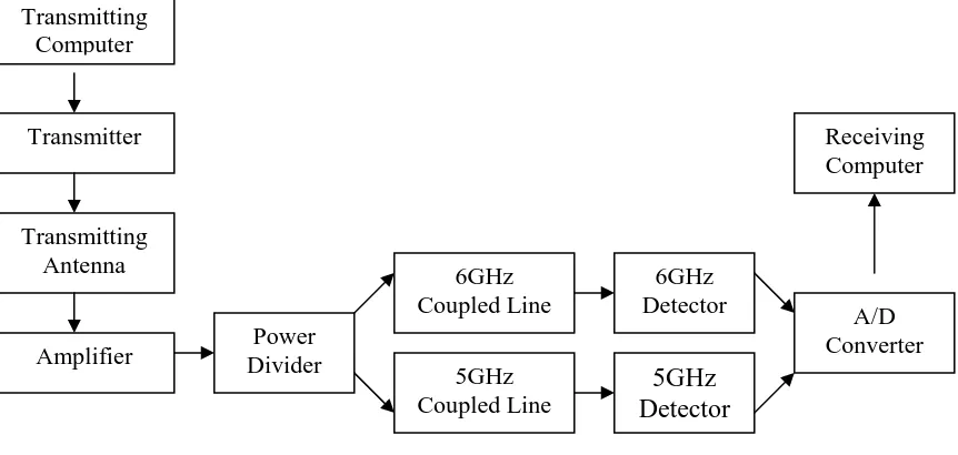
Figure 1.1 shows a system level diagram of the wireless local area network. The
reduction in the signal due to losses during transmission, reception and power
dissipation in circuit components must be compensated by using a device to provide
[image:19.612.116.547.463.668.2]sufficient gain for the receiver circuit.
Figure 1.1: System level diagram of the wireless local area network. Transmitting
Computer
Transmitter
Transmitting Antenna
Amplifier Divider Power
2
As the name implies, it is used to amplify the low level signal that presents at the
receiver input to level that is well above the noise threshold of the subsequent stages,
without significantly contribute to that noise itself. Low Noise Amplifier can be
considered as a key component and it performance has significant impact to the whole
communication system, because the noise figure of the receiver is dominated by the first
stage of the cascaded amplifiers. The noise of the Low Noise Amplifier will pass to the
subsequent stages which then be reduced by the gain of the Low Noise Amplifier and
the gain of rest of the cascaded amplifiers. To ensure the retrieval of signal is possible in
the later stage of the communication systems, it is necessary that the Low Noise
Amplifier is able to amplify the received signal to an acceptable power without adding
much noise or cause distortion to the received signal. [1]
In this project, a high-performance, low-cost, highly repeatable two-stage low
noise amplifier (LNA) for use in 5GHz to 6GHz wireless applications is presented. The
final product used throughout this project is BFP640 NPN Silicon Germanium RF
transistor, for WLANs systems and cordless phones using the 5GHz to 6GHz frequency
range. The BFP640 silicon germanium RF transistor offers a high performance,
power-efficient solution for a broad range of high-frequency low noise amplifier (LNA)
designs.
This project will deals mostly with Low Noise Amplifier design, fabricating and
testing the amplifier using microstrip technology. The approach taken to design the
amplifier involves a series of chronological steps. No design is complete without some
desired goals. The design specifications for the low noise amplifier were as follows: [9]
Frequency Band = 5-6GHz
Noise Figure > 1.2dB
Power Gain > 15dB
S11 and S22 < -15dB
3
1.2 PROBLEM STATEMENTS
In general, the RF performance of the Low Noise Amplifier is very good as it
able to achieve the required gain and provides low noise figure. As for the different
biasing circuit, active biasing does not offer much advantage over the passive biasing
circuit. The only improvement recorded is the noise figure performance of the Low
Noise Amplifier with active biasing circuit. The bipolar junction transistor was the first
solid-state active device to provide practical gain and noise figure (F) at microwave
frequencies.
The matching networks can be changed to lump elements for space reduction and
cost saving. Low Noise Amplifier usually implies RF/wireless applications. But noise is
also a critical consideration for lower frequency analog applications. In order to avoid
this, the purpose of this project comes in. To select an appropriate amplifier, first
understand the noise parameters for a particular application and then determined whether
an amplifier is indeed low noise.
Although low noise amplifier (LNA) performance was extremely good
nowadays, the design engineer still had to make some complex system trades. Many
LNA were large, heavy and consumed a lot of power. For an example in satellite ground
terminals, low noise performance, lighter weight, low power and high reliability of LNA
are required. Unfortunately, it is not always achieved because of limitation in some
factors.
1.3 OBJECTIVES
The objective of the research project is to design, simulate and fabricate Low
Noise Amplifier (LNA) at 5 to 6 GHz. The designed require low noise figure, sufficient
4
The gain is expectedly higher than 15 dB and noise figure value must below than 1.2dB.
The designed LNA should able to work under unconditionally stable state along the
frequency band. Finally, the designed LNA should work properly in the Wireless Local
Area Network (WLAN) environment.
1.4 SCOPES OF WORK
Scope of this project can be divided into three parts:
1. Simulation – It will be done by varying parameters using Advanced Design
System (ADS) in order to get the required results which are close to the
theoretical results.
2. Fabricating – The fabrication of the Low Noise Amplifier will be done using
Microstrip, PCB laminate (e.g.: Standard low cost FR-4), aluminums sheet,
etching facilities.
3. Test analysis– A test analysis is the last stage in this project. The performance of
the designed amplifier circuit is verified on board using the RF testing equipment
such as the vector network analyzer and cable.
1.5 THESIS STRUCTURE
The thesis is divided into five chapters and covers the research works that have
been through for Low Noise Amplifier circuit design. Chapter 2 reports the literature
review of the basic concepts in Low Noise Amplifier circuit design. Chapter 3 describes
the design and simulation process. The Advance Design System (ADS) software was
used to do the design and simulation process. The simulation and measurement results
are reported in Chapter 4. This chapter also includes discussion from simulation and
measurement results. Chapter 5 concludes the research work and gives suggestion for
5
CHAPTER II
LITERATURE REVIEW
2.1 INTRODUCTION
One of the largest growth areas in electronics over the past decade has
undoubtedly been in applications of wireless communication. Semiconductor
technologies have been a key to this growth, bringing added convenience and
accessibility through advantages in cost, size, and power dissipation. Wireless products
and systems thrive on this increased utility, the commercial momentum of which has
been fueling further investment in integrated circuit designs and technology. The
resulting advancement in system capabilities has developed greater interest and
receptiveness on the part of the consumer, leading to more applications being
envisioned, and necessitating more available spectrum to support the wireless
infrastructure. [6]
To obtain this added bandwidth and alleviate interference, the frequencies of the
communication channels are necessarily edging upward, placing yet more demands on
the technologies used to implement the wireless systems. Several recently opened ISM
bands in the 5-6GHz range have been allocated for unlicensed operation of broadband
6
This chapter develops some basic principles used in the analysis and design of
microwave Low Noise Amplifier (LNA).The most important design considerations in a
microwave Low Noise Amplifier are stability, power gain, and bandwidth, noise, and dc
requirements. Research has been done to study:
- Low Noise Amplifier properties (briefly).
- Low Noise Amplifier design.
- Transistor specifications.
- Types of software (e.g.: Microwave Office and Advanced Design System
[image:24.612.187.527.359.548.2](ADS)).
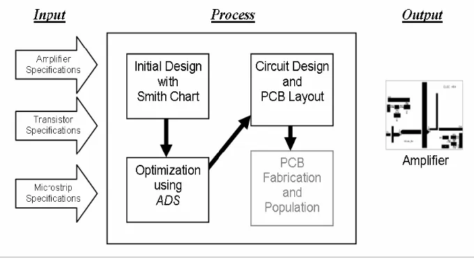
Figure 2.1 shows a design flow of this project.
Figure 2.1: Design flow of the project.
This chapter will discuss about microwave transistor, DC biasing, two port