DOI: 10.12928/TELKOMNIKA.v14i3.3644 867
Critical Condition in CuInAlSe2 Solar Cell Absorbers
Sujarwata*1, Fianti2, M.I. Amal3, J.Y. Jung4, S.H. Lee5, K.H. Kim6
1,2Jurusan Fisika, Universitas Negeri Semarang,
Kampus Sekaran Gunungpati Semarang 50229, Indonesia, fax: +62248508034
3
Lembaga Ilmu Pengetahuan Indonesia, Tangerang Selatan, Indonesia
4,5,6
Materials Science and Engineering, Yeungnam University, South Korea, Gyeongsan 712749, fax: +82538104628
*Corresponding author, e-mail: [email protected], [email protected], [email protected]
Abstract
The CuInAlSe2 (CIAS) phase offers a wide band gap which allows some adjusting in band gap energy for high solar cell efficiency. Most research design a Cu-deficient condition for more favorable electronic properties, but there is still a question about the limit of Cu-deficiency in CIAS that allows good properties of solar cell absorber. In this research, we found the critical condition of Cu defficient in CIAS by preparing and analyzing the CIAS thin film absorbers. The thin film precursors were tailored using PLD system with a certain stacking order of layer-by-layer elemental film deposition and then selenized via a solid state reaction to form CIAS phases. The prepared thin films were analyzed for their composition, structure, electrical-optical properties, and morphology. The results show that CIAS thin film absorber in Cu-deficient condition still can be performed in single phase structure until 18 at.% of Cu/CIAS with high band gap energy, high charge carrier concentration, and good morphology. In addition, CIAS composition in ~17 at.% of Cu/CIAS becomes a critical condition in having good thin film absorber properties.
Keywords: CIAS, Cu-deficient, PLD, thin film
Copyright © 2016 Universitas Ahmad Dahlan. All rights reserved.
1. Introduction
Harvesting solar energy becomes an interesting alternative for renewable, abundance, and clean energy source in research. Otherwise, the output power of the panels of solar cells varies with solar irradiation and temperature, which affect its efficiency. There are many ways to increase the efficiency of solar cells. One of them is using a control technique, Maximum Power Point Tracking (MPPT), that extracts the maximum available power from the panels of solar cells [1, 2] and its advanced technology of MPPT is employing fuzzy logics which is applied on the controller [3]. Beside the harvesting technology, research also developed in its materials of preparing the solar cells and the most important part of solar cells is the absorber layer which has a duty in corverting the light energy from solar radiation in to voltage of electricity.
The CuInAlSe2 (CIAS) is an absorber material which its phase offers a wide band gap of
1.0 eV (CuInSe2) to 2.7 eV (CuAlSe2) [4, 5]. This property allows the formation of CIAS by some
adjusting to achieve high efficiency of solar cells; however, most researchers and solar cell industries are not very interested in CIAS, because we need to pay much attention and effort in single-phase CIAS formation. Grain size is one of many keys of high efficiency, and large grain size is preferred for solar cell application [6]. At 500 oC, CuxSe quasi-liquid phase in Cu-rich
condition has a high solubility of In and Ga for a high diffusion [7]. The Cu2-xSe segregating at
the surface and grain boundaries becomes a fluxing agent during the growth process and helps in the formation of large and compactly packed grains [8]. Thus, layers grown under Cu-rich conditions usually have substantially larger grains than those grown under Cu-poor conditions [9].
research, thin film preparation was started in the Cu-rich stage for preferable grain size and ended in the In-rich stage to have Cu-deficient CIAS for favorable properties [6, 8].
In the previous research, we were success in CIAS single phase formation by PLD and selenization with thin film composition 1.2-0.8 of Cu/IIIA or 17-23% of Cu/[CIAS] [14]. By this research, we would continue the previous research to find the critical condition in the composition of Cu-deficient of CIAS at the least Cu composition of previous CIAS thin film. We prepared 2 CIAS thin films with Cu composition ~17% of Cu/[CIAS] and analyzed the properties. The precursors were tailored using PLD system with a certain stacking order of layer-by-layer elemental film deposition. They were then selenized via a solid state reaction to form CIAS phases using different heat treatment steps.
2. Research Method
2.1. Pulsed Laser Deposition (PLD)
The precursors were prepared using three bulk source targets: 4 N Cu, 4 N Al, and mixed In-Se (30 at% of In/[In+Se]). The substrates were 1.3 cm × 1.2 cm × 0.1 cm glasses that were sequentially cleaned with acetone, ethanol, de-ionized water, and ethanol in a Branson 2510 ultrasonic cleaner (40 kHz). The precursor films were deposited using the PLD technique.
The laser source was an ArF Excimer (λ = 193 nm), the distance between targets and
substrates was 50 mm, the laser pulse delay was 308 µs, the working pressure in the PLD chamber was 3.7 × 10⁻⁶ Torr, and the process was run at room temperature. The precursor compositional ratio was controlled by adjusting the deposition time interval, andthe precursor composition of the two precursors was designed to be the same using the same parameters. The stacking order of the elemental film deposition can be seen in Figure 1.
Figure 1. Elemental Stacking Order of the Precursors
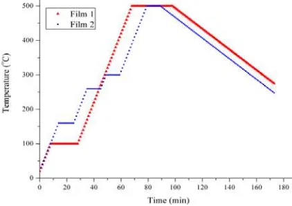
Figure 2. The Heat Treatment Steps in the Selenization Process
2.2. Selenization
The selenization (Figure 2) was run at atmospheric pressure using an Ar gas flow and 1.25 g of Se chips was added to the furnace tube.
3. Results and Analysis 3.1. Morphology
Al-doped Cu can arrest Cu oxidation (the formation of CuO2), improve Cu adhesion to
SiO2 and improve film stability on SiO2 [15]. This improved stability occurred due to the
decreasing diffusion transport into SiO2 since Al is transported through copper at a relatively low
temperature (275–300°C) [15]. Annealing Cu/Al/SiO2/Si will protect the underlying Cu from
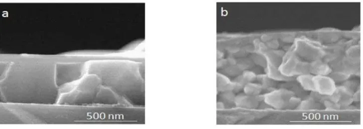
oxidation, even upon heating at 350°C in air for 4 hours [16]. Both Al and Cu have good adhesion to glass, and Cu diffuses into glass at high temperatures [17]. This Cu diffusion can be solved by using Mo, where Mo improves the Cu adhesion and avoids Cu diffusion into the glass [18]. Thus, Al deposition on the glass will prevent Cu oxidation, improve the film adhesion to the glass, and decrease Cu diffusion into the glass. Figure 3 shows that the films have good adhesion to the substrates.
Figure 3. Cross Sectional Images of (a) Film 1 and (b) Film 2
The mixed In-Se elemental layer let In and Se form binary InxSey in selenization. Since
the InxSey formation could occur prior to the CIAS formation, the In was kept from evaporating
due to having the lowest melting point. Moreover, a mixed In-Se layer was put between the two Cu layers to allow the Cu and In to diffuse well because of the Cu preference in moving frequently by vacancy-mediated surface diffusion, even at room temperature, and Cu tendency in performing self-interstitial [19]. Further, this layering also let defect pair formation where defect pairs such as (2V-Cu + In
2+
Cu) and (2Cu -2
In + In 2+
Cu) have low formation energies [20].
Moverover, this defect pairs play a big role in energy conversion, light to electricity.
Film 1 was selenized through two temperature holding steps: 100°C for 20 min and 500°C for 30 min. The first step homogenized the film composition and the second step let the CIAS form. Film 2 was selenized through four steps (160°C, 260°C, 300°C, and 500°C), each of which was run for 10 min. The 160°C step was held to melt the in for better In diffusion in the liquid state. The 260°C step was held to let the InSe form. The 300°C was held to let the In2Se3
and CuxSey form and the Al diffuse into the Cu layer. The film composition can be seen in Table
1. The Cu-poor condition is more preferable for the p-type semiconductor. However, the Cu incorporated in the CIAS was less than 18%. Since the grain growth fluxing agent (CuxSe) was
lacking, this condition was a trigger for unsuccessful grain growth resulting large grain boundaries. As such, if the film had single-phase CIAS (meaning all of elements were incorporated in the CIAS phase), the grains would be small (Figure 3b).
3.2. Structure
Table 1. Film Composition
Film Element (at.%) Cu/(In+
Al)
Cu In Al Se
1 17.12 22.74 0.22 59.93 0.75
2 17.54 19.83 0.22 62.41 0.87
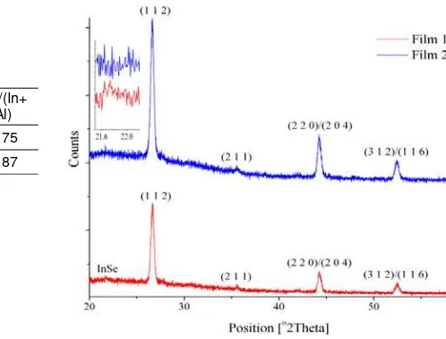
Figure 4. X-ray Diffraction Patterns of film 1 and 2
The CIAS 2θ lies between CIS and CAS 2θ and shifts according to the Al amount in the CIAS. Thus, the higher the Al content, the closer to the CAS 2θ and vice versa [16], [26, 27]. Since the In and Al compositional ratios in each precursor were the same, the formation of InSe layer in film 1 caused reduction of the In incorporated into the CIAS structure. Hence, the In ratio in the CIAS structure of film 1 was less than that in film 2 since all of the In in film 2 was used for CIAS formation, meaning that a higher Al ratio incorporated into film 1 than that in film 2. These phenomena influenced the XRD pattern in the CIAS identification. Therefore, even the 112 peaks of films 1 and 2 revealed CIAS (by CIS standard), but the diffraction peaks were different, consequently CIAS peak of film 2 was closer to the CIS peak than that of film 1.
This critical condition in film morphology can be seen in Figure 3. The grain of film 1 was larger than that of film 2, with greater width than height. The InSe phase can be seen as a flat layer on the grains of film 1 (Figure 3a). On the other hand, the grains of film 2 were small (Figure 3b), but the XRD pattern gave only CIAS peaks, meaning that theheat treatment of film 2 induced CIAS formation without any secondary phase in the Cu-deficient condition. Having small grains does not mean that the allowed time for CIAS grain growth was not sufficient to yield optimum grain size in film 2. The small grains were yielded by the Cu-deficient condition resulted in unsuccessful grain growth.
The thickness of films 1 and 2 was different, as film 1 was thinner than film 2. The thicker film means the more film mass. The InSe-phase rising and the film thickness difference were caused by the heat treatment difference. First, the film 1 composition was homogenized at 200°C for 20 min, enough time for the In moving up to the top layer and down to the bottom. At 500°C, the CIAS formation was promoted for 30 min. After the CIAS formation, the heating continued. This exceeded time required for CIAS formation induced CIAS decomposition to the InSe phase. The InSe was created from unbounded in, which resulted in decomposition and homogenization, on the surface that trapped the Se from the environment. Figure 3 shows that the grains of film 1 were much bigger than those of film 2 and revealed that the CIAS formation was more than sufficient to grow the CIAS.
3.3. Electrical Optical Properties
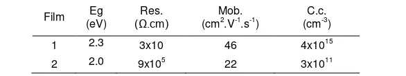
The electrical properties of the films are shown in Table 2. Since there was a secondary InSe phase and its layer was thick enough (relatively compared to the grain height), it played a big role in influencing the electrical properties of film 1. Consequently, the films can not be compared; the electrical properties of the films were different. Otherwise, the electrical properties of film 2 can still be analyzed, which gave clausal thinking in the CIAS study.
At room temperature (without solar illumination), the equilibrium Fermi level (Ef) of the grain boundary is closer to the conduction band edge than to the valence band edge, indicating that carrier-type inversion is occurring at the grain boundary [28]. Thus, the detected carrier concentration of film 2 was low (~1011 cm-3) compared to the good absorber from other reports, ~1016–1018 cm-3 [29, 30]. Materials could include insulators, semiconductors, and conductors depending on the band gap energy between the valence and conductive bands. The more conductive materials, the lower band gap energy. The small amount of Al incorporated in the CIAS will provide a higher band gap compared to Ga in CIGS [4], but the Al amount in this CIAS is only 0.22 at%, so the high band gap was not caused only by the existence of the Al content but also by the Cu-deficient and Se-rich conditions. Therefore, film 2 had high band gap energy of 2.0 eV (Table 2).
Table 2. Film Resistivity (Res.), Mobility (Mob.), and Carrier Concentration (C.c.)
Film Eg
The CIAS phase can be prepared with ~17 at% Cu through precursor preparation in the PLD system and selenization. The Cu-deficient became a critical condition in the InSe secondary-phase formation of the selenization process. Here, the CIAS single-phase film can be reached and, on the contrary, grain growth becomes the constraint. On the other hand, the large grain size in CIAS can be reached along with InSe formation.
Acknowledgements
We would like to thank to Dr. Rachmat Adhi and Prof. Kamsul Abraha for our discussion and sharing experiences in research. This research was supported by DIKTI Indonesia and a grant from Yeungnam University, South Korea.
References
[1] Alik R, Jusoh A, Sutikno T. TELKOMNIKA Telecommunication Computing Electronics and Control. 2015; 13(3): 745.
[2] Jusoh A, Mohammed OJEI, Sutikno T. TELKOMNIKA Telecommunication Computing Electronics and Control. 2015; 13(1): 1.
[3] Lubis AJ, Susanto E, Sunarya U. TELKOMNIKA Telecommunication Computing Electronics and Control. 2015; 13(1): 32.
[4] Marsillac S, Paulson PD, Haimbodi MW, Birkmire RW, Shafarman WN. Appl. Phys. Lett. 2002; 81: 1350.
[5] Dwyer D, Repins I, Efstathiadis H, Haldar P. Sol. Energy Mater. Sol. Cells. 2010; 94: 598.
[6] Hayashi T, Minemoto T, Zoppi G, Forbes I, Tanaka K, Yamada S, Araki T, Takakura H. Sol. Energy Mater. Sol. Cells. 2009; 93: 922.
[7] Walter T, Schock HW. Thin Solid Films. 1993; 224: 74. [8] Dhere NG. Sol. Energy Mater. Sol. Cells. 2006; 90: 2181.
[9] Hetzer MJ, Strzhemechny YM, Gao M, Contreras MA, Zunger A, Brillson LJ. Appl. Phys. Lett. 2005; 86: 162105.
[10] Munir B, Wibowo RA, Kim KH. Solid State Phenomena. 2008; 135: 99. [11] Perng DC, Chen JW, Wu CJ. Sol. Energy Mater. Sol. Cells. 2011; 95: 257. [12] Dhanam M, Kavitha B, Velumani S. Mater. Sci. Eng. B. 2010; 174: 209. [13] Kim KH, Fianti. Journal of Korean Physics Society. 2012; 60: 2001.
[19] Zang SB, Wei SH, Zunger A, Yoshida HK. Phys. Rev. B. 1998; 57: 9642.
[20] Jost S, Hergert F, Hock R, Purwins M, Enderle R. Phys. Stat. Sol. A. 2006; 203: 2581. [21] Halgand E, Bernede JC, Marsillac S, Kessler J. Thin Solid Films. 2005; 480-481: 443.
[22] Chandra GH, Udayakumar C, Rajagopalan S, Balamurugan AK, Uthanna S. Phys. Status Solidi A. 2009; 206: 704.
[23] Garcia JL, Maffiotte C, Guillen C. Sol. Energy Mater Sol. Cells. 2010; 94: 1263. [24] Kavitha B, Dhanam M. Journal of Ceramic Processing Research. 2009; 10: 652.
[25] Umezawa A, Yasuniwa T, Miyama A, Nakanishi H, Sugiyama M, Chichibu SF. Phys. Status Solidi C. 2009; 6: 1016.
[26] Dhananjay, Nagaraju J, Krupanidhi SB. Solid State Commun. 2003; 127: 243. [27] Rau U, Taretto K, Siebentritt S. Appl. Phys. A. 2009; 96: 221.
[28] Rockett A, Birkmire RW. J. Appl. Phys. 1991; 70: R81.