Low Cost Electro-deposition of Cuprous Oxide P-N Homo-junction Solar
Cell
Faiz Arith
1,a, S.A.M. Anis
2,b, Muzalifah Mohd Said
1, Cand M. Idzdihar Idris
1,d 1Faculty of Electronics and Computer Engineering, Universiti Teknikal Malaysia Melaka (UTeM), Melaka, Malaysia.
2
Faculty of Science and Technology, Universiti Kebangsaan Malaysia, UKM, Bangi 43600, Selangor, Malaysia.
a
[email protected], [email protected], [email protected], d
[email protected] Keywords: Cu2O, ITO, AM1 light, XRD
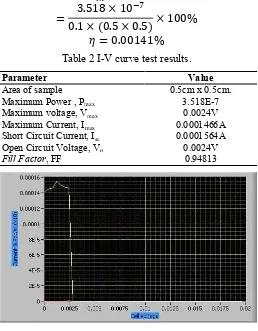
Abstract. Most of the photovoltaic industry uses wafer of single-crystal and poly-crystal silicon as a material of their photovoltaic (PV) modules. However, the cost of these modules is high due to the material and processing cost. Cuprous oxides (Cu2O)have several features that suitable for future photovoltaic applications. Cu2O can be prepared with simple methods at very low cost. Cu2O p-n homojunction solar cell is a device that converts sunlight to electrical energy, consists of two similar materials for its p-n junction, which is Cu2O. The p-type and n-type of Cu2O thin films are then fabricated to produce solar cells. Other layers aluminium and glass substrate coated with indium tin oxide (ITO) need to be added as a contact for electrons movement. In this study, p-type Cu2O, n-type Cu2O and p-n junction are prepared in order to become accustomed for solar cell applications. To achieve the optimum deposition conditions, p-n junction solar cell is prepared by two-steps electrochemical deposition process. The result from x-ray diffraction (XRD) shows that the peak is dominated by CuO (1, 1, 1). P-n junction is in between the p-type and n-type of Cu2O layer. Al has the thickness of 427.5nm. The second and the third layer are p and n –type of Cu2O, which have the thickness of 106.9nm and 92.3nm, respectively. Finally the thickness of ITO layer is 131.1nm.An absorption experiment at AM1 light is performed in order to get the I-V curves, and in fact, to study the electrical solar cells p-n homojunction. Based on I-V curve test, the level of energy conversion of cell is 0.00141% with fill factor, FF 0.94813 which proved that Cu2O p-n homojunction solar cell can be fabricated and produced at very low cost and well function.
Introduction
Currently the photovoltaic market production is dominated by silicon based solar cell. Due to their fabrication process that required sophisticated and high cost of equipment, the electricity genreration cost of silicon based solar cell is difficult to compete with fossil energy. There is exit way to overcome this matter by producing solar cell from cheap material with simple method [1].
Cu2O thin films can be prepared with simple methods at a very low cost by using electro-deposition method [2]. The cuprous oxide is formed from non-toxic elementswhich are copper and oxygen so the supply is easily available in the world [3]. Their absorption coefficient is goodfor light that have greater energy than energy bandgap. Energy bandgap for cuprous oxide is 1.9eV at room temperature[4].It have suitable majority carrier mobility and and minority carrier diffusion length in the micrometer range. By reducing cost, cuprous oxide has potential to be used in the new generation of dual solar cell which is polycrystalline multi-junction solar cell and intermediate band solar cell[5-6].Both of these new concepts seem promising to increase solar cell efficiency in the future.
Multi-junction solar cell consistseveral layers of thin films materials with different energy bands purposely to absorb more solar radiation of light waves[5, 7-8]. Short-wavelength solar radiation will be absorbed on the top layer while the remainingwavelengths of light rays are absorbed by the lower layers. Cuprous oxide thin film with high energy band of 1.9eV can be used as a top layer of this multi-junction solar cell.
In the intermediate band solar cell, more light waves can be absorbed by the existence of an intermediate band in the material. The intermediate band solar cell is formed by doping with impurity elements that will produce a deep energy level in the band gap. In this way the absorption of radiation with energy less than the band gap occurs through two mechanisms. First, when the photon with less energy than the band gap is absorbed, electrons will excit from the valence band to the intermediate band. Then, the absorption of another photon also with less energy than the band gap, electrons wills excit from the intermediate band to the conduction band. These mechanisms complete the absorption of electron from valence band to conduction bandwith less energy than the band gap[9].
Cu2O solar cell is tools that use to convert sunlight, or magnetic radiation to an electric energy. This p-n junction solar cell consists of two similar materials which are cuprous oxide Cu2O the p-type semiconductor. By using electrochemical deposition method, the Cu2O can be turn to be n-type Cu2O. The optimum oxygen entrancecan be achieved by controlling the pH value, temperature and voltage potential value[10].To facilitate the realization of the main research objective, 3 sub-objectives are defined as below:
i. To design and fabricate p-type Cu2O, n-type Cu2O and p-n homojunction Cu2O solar cell. ii. To determine p-type Cu2O, n-type Cu2O and p-n homojunction Cu2Ofeature and characteristics as a solar cell.
Methodology
In this study, p-type, n-type and p-n junctions have been prepared in order to be use for solar cell application. Homo-junction solar cells are made with Cu2O electrochemical reduction method to achieve the optimum deposition conditions. Light absorption experiment at AM1 has been conducted to obtain I-V curve, thus the electrical properties of p-n homojunction solar cells can be studied. Crystal characterization was also performed using XRD. By using scanning electron microscopy (SEM) technique the surface, cross-section and microstructure of the film reduction can be characterized [11-12]
Fabrication of CU2O thin film
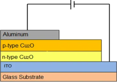
Cu2O thin film consists of four layers with different material, ie, ITO, Cu2O n-type, p-type Cu2O and aluminum as shown in Fig. 1. Several methods are used to provide these layers. For the first layer, completed ITO that coated with glass substrate is used.
Figure 1 Cross sectional diagram of Cu2Othin films solar cell
Electron deposition method is used to produce Cu2O layer of n-type and p-type. The electrodeposition process consists of three types of electrodes [10, 13]. In this study, the working electrode (WE) is coated with ITO glass substrate. Reference electrode (RE) is Ag / AgCl / NaCl while platinum sheet as counter electrode (CE)
Surface structure is characterized by using Dino-Lite AM311S to view the structure of ITO layer. This device also been used before and after the deposition process. After that, radio frequency (RF) sputtering machine is performed to grow the aluminum (Al) layer on top of n-type layer. Al layer is used to allow electrons to flow from the p-type layer as ohmic contact.
Results
Cu2Ohomojunction thin films. Fig. 2(a) show the surface of ITO coated the glass substrates. ITO is a transparent overlay when viewed with the naked eye. Fig.2(b) shows the sample surface of ITO layer after the deposition process by using aqueous solution of n-type. Fig.2(c) shows the state of the surface after the deposition process using a solution of p-type layers on n-type. This layer is visible yellow and has a structure like an orange peel.
(a) (b) (c)
Figure 2 The glass substrate’s surface with the (a) layer of ITO, (b) layer of n-type deposited on ITO layer, (c) layer of p-type deposited on n-type layer.
Analysis and Discussion
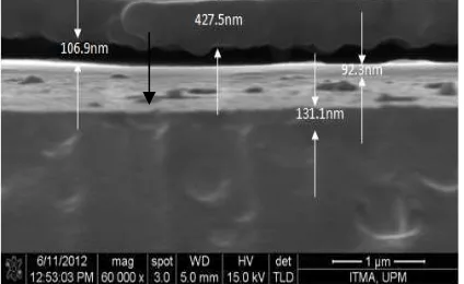
Field Emission Scanning Electron Microscopy (FESEM). FESEM is performed to obtain the thicknessof each layer in Cu2O thin film [16]. Based on the Fig.3, the first layer thickness is 427.5nm, 106.9nm second layer, third layer 92.3nm and 131.1nm fourth layer. The cross section shows the uneven layers especially the second layer.
Figure 3 FESEM image that shows the thickness for each layer of Cu2O p-n homujunction solar cell.
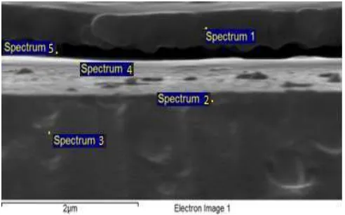
Figure 4 Spectrums representing each layer of Cu2O thin film.
Table 1 Types of layer and its thickness for each spetrum
Spectrum Type Thickness
1 Aluminum 427.5nm
2 ITO 131.1nm
3 Glass Substrate 1.35mm
4 n-type Cuprous Oxide 106.9nm
5 p-type Cuprous Oxide 92.3nm
X-Ray Diffraction (XRD). XRD spectra for Cu2O thin films are shown in Fig.5. Notably, there are some differences peak heights. All tops use the same wavelength which is 1.5406. The most significant peak height of CuO with Miller indices (1,1,1). It has the intensity at 2θ = 32.4 a.u 36,595. CuO has a value of a = 4, b = 4, and c = 4. Z value for the CuO is 2 with space group Fm-3m (225). Copper oxide, Cu8O (2,0,0) can also be seen at 2θ = 13.7 au intensity of 44,697 where it is on the right-most peak with Bmm2 space group (38). Z value for Cu8O is 2. In addition, Al (2,0,0) as a conductive layer can also be seen at 2θ = 44,037 with the intensity of 6.28 au. Al is in the space group C2 / c (15) and has a Z value of 2. The left-most peak represents Cuprite, Cu2O (1,0,0)[16]. Cu2O has space group Pn.3m (224) at 2θ = 11.0 au and the intensity of 36,595. The low peaks are combination of elements in the glass substrate and ITO layer. For example, at 21,529 and the intensity of 2θ = 3.68 au Indium Tin Oxide or In4Sn3O12 elements is involved. The Z value for this element is 3 and has the space group R-3 (148).
Figure 5 XRD pattern of Cu2O p-n homujunction solar cell.
=
Homojunction p-n cuprous oxide thin films have been prepared by electrodeposition method. The thickness of each layer cuprous oxide thin films has been identified. In addition, the feature crystal composition of each layer, the electrical properties and efficiency of Cu2O thin films have also been discussed.
Cu2O thin films p-n homojunction has 4 layers on the glass substrate. The first layer is ITO on glass substrates. Sediment deposited on ITO layer is a layer of n-type Cu2O subsequent deposition of p-type Cu2O layer. Conductor layer, a layer of Al, produced on p-type Cu2O layer. P-n junctions are between the layers of p-type and n-type of Cu2O layer. Al layer thickness is 427.5nm. Next, the second layer and the third layer is p-type and n-typeCu2O respectively 106.9nm 92.3nm thick. ITO layer has a thickness of 131.1nm. Cross section shows the uneven layers especially the second layer. This is because the process is not uniform during the deposition method is done.
References
[1] A. V. Shah, H. Schade, M. Vanecek, J. Meier, E. Vallat-Sauvain, N.Wyrsch, U. Kroll, C. Droz1 and J. Bailat, Thin-film Silicon Solar Cell Technology, Progress In Photovoltaics: Research And Applications 12:113–142 (2004)
[2] Abdu, Y. Copper(I) Oxide (Cu2O) Based Solar Cells – A Review, Department of Physics, Bayero University, Kano (2009) p. 8-11.
[3] A. Goetzberger, Material Science and Engineering Vol 40, (2003), p. 1-46
[4] Georgieva, V. and Ristov, M. Electrodeposited cuprous oxide on indium tin oxide for solar applications. Solar Energy Materials and Solar Cells, Vol. 73 (2002), p. 67
[5] Biccari, F, Defects and Doping in Cu2O, Ph.D. thesis Sapienza – University of Rome, Rome 2(2010).
[6] R.H Bube, K.W Mitchell, Research Opportunities in Polycrystalline Compound Solar Cells, J Electron. Mater, 22 (1993)
[7] Alvin, D. Photovoltaic: Vleas Power for the 21st Century, USA, 90: 2170-2180 (2006)
[8] Boer, K.W. 1992. Survey of semiconductor Physics, Vol.lI, Van Nostrand Reinhold, NewYork, p-820
[9] Luque, A. and Marti, A. Increasing the efficiency of ideal solar cells by photon induced transitions at intermediate levels. Physical Review Letters, Vol 78 (1997)
[10]Wang, L. Preparation and Characterization of Properties of Electrodeposited Copper Oxide Films, Doctor of Philosophy, Faculty of the Graduate School, The University of Texas at Arlington (2006)
[11]Sear, W.M. and Fortin, E.J Preparation and Properties in Polycrystalline Compound Solar Cells, J Electron. Mater, 22:17 (1993)
[12]Ito, T., Yamaguchi, H., Okabe, K., and Masumi, T. 1998. Single-crystal growth and characterization of Cu2O and CuO. Journal of Materials Science, 33 (1998), 3555
[13]Abdul Mateen, Some Methodogies Used for the Sysnthesis of Cuprous Oxide: A Review. Faculty of Materials Science and Engineering, Ghulam Ishak Khan Institute of Engineering Sciences and Technology, Pakistan. (2008)
[14]Daltin, A.L. Kinetics of Cu2O Electricrystallization under Magnetic Field, France. 54:5813-5817 (2009)
[15]Johan, M.R, Annealing Effects on the Properties of Copper Oxide Thin Films Prepared by Chemical Deposition, Kuala Lumpur 6: 6094-6104 (2011)